
Abstract
Patterning using a focused ionizing radiation beam provides a high spatial resolution but is not feasible when creating large arrays of microstructures. We propose the optimization of x-ray lithography parameters to create submicropores in a low-sensitivity material (polyethylene terephthalate) using a wide x-ray beam. This optimization results in the fabrication of regularly arranged micropores with a high aspect ratio (over 20) and diameters of up to 0.4 µm across a large substrate area (up to several square centimeters).
Export citation and abstract BibTeX RIS

Original content from this work may be used under the terms of the Creative Commons Attribution 4.0 license. Any further distribution of this work must maintain attribution to the author(s) and the title of the work, journal citation and DOI.
1. Introduction
Thin-film-based microporous filters exhibit important properties. They can be used to separate bacteria or insoluble particles in biological or chemical solutions [1]. They can also be used to allow vacuum ultraviolet and soft x-rays while blocking visible light [2] as well as serve as a matrix for various chemical reactions, such as oxidation and deoxidation [3]. To amplify infrared radiation, matrices of pores several hundred nanometers in diameter are filled with optically active compounds that generate radiation, the wavelength of which is determined by the optical properties of the filler [4].
Arrays of micropores with diameters in the submicrometer range and lengths from one to hundreds of microns provide the abovementioned properties. Such micropores can, in a technical sense, be classified as microstructures with high aspect ratios. Such structures are produced by irradiating a polymer film with accelerated heavy ions and subsequent etching of the destroyed material along the ion tracks. However, the random distribution of micropores over the film causes them to overlap, which drastically reduces the selective properties of filters [5]. On the other hand, a device that exposed the initial film to single ions by simultaneous scanning of the rectangular film to the ion beam, can provide low productivity [6]. Therefore, it would be beneficial to create large arrays of non-overlapping, compactly arranged micropores in one 'shot'. As a solution, it was proposed to replicate arrays of micropores by transferring the image of a stencil mask using x-rays [7]. To this end, synchrotron radiation (SR) should be used, the spectrum of which is wide enough to select the actual range of photon energies, and the high collimation of the x-ray beam will provide low projection distortions of the pattern over a large area.
The results obtained are based on the ability of polyethylene terephthalate (PET) to ensure high selectivity for etching after exposure to heavy atom ions [8] and on the formation of high-aspect-ratio microstructures by deep x-ray lithography under conditions optimized for highly collimated x-rays provided by SR sources. These conditions are presented in several works [9–12], which have paved the way for the x-ray lithography used in the present work. This coincided with the development of x-ray resists [13, 14] optimized for the lithographic process, namely those with submicrometer resolution and relatively high sensitivity. X-ray-lithography was further developed in the works by Guckel and Betz [15, 16].
The properties of polymethyl methacrylate (PMMA) and negative tone resist SU-8 have been well studied (table 1). These polymers are typically used for elements in micromechanics, microhydraulics, and microoptics [17, 18] that do not impose extremely high requirements.
Table 1. Properties of PMMA, SU-8, and PET.
| Material/properties | Tensile strength (MPa) | Glass transition temperature (Tg) (°C) | Melting temperature (Tm) (°C) | Radiation resistance (MGy) |
|---|---|---|---|---|
| PMMA | 70 [19] | 105 [19] | 160 [19] | 0.05 [20] |
| SU-8 | 19–16 [21] | >200 [22] | ∼380 [22] | 4 [23] |
| Polyethylene terephthalate | 53 [24] | 67 [25] | 265 [25] | 5 [23] |
Therefore, materials with unique properties that enable their use in critical conditions are of interest. For example, in addition to high radiation resistance, PET is resistant to microbial attack and does not degrade under normal environmental conditions [26] nor in aqueous acidic and alkaline solutions; it requires very severe chemical degradation approaches and vapor gas treatment, such as sterilization or cooking [27, 28]. Due to the outstanding barrier properties of PET, it is used in film-making applications, such as photographic, magnetic, x-ray, and metalized films, as well as electrical insulation [29]. PET films also exhibits high transparency in the visible range of the spectrum. In contrast, SU-8 is selectively transparent, not stable in aqueous alkali solutions, and the antimony atoms it contains can cause biocompatibility problems.
In addition, the high etching selectivity of PET exposed to x-rays has been successfully demonstrated by the creation of microstructures in thick films [30] as well as the formation of microporous membranes up to 2 µm thick [7, 31], which ensures submicrometer spatial resolution in the process. This was achieved by investigating the PET irradiation conditions and thermal fields in the irradiated areas of the film as well as the effect of alkaline-water etching of the destroyed polymer. However, optimization of the above technology has not been previously discussed. The results of this study are discussed here.
2. X-ray lithography method for fabrication of submicron structures
2.1. X-ray lithography station
An advanced LIGA station on the VEPP-3 synchrotron source is shown in figure 1 [32]. The x-ray beam arrived at the exposure chamber from a shifter placed in a straight section of the VEPP-3 storage ring. The irradiation source was located at a point where the electron orbit showed maximum deviation from the unperturbed trajectory. This corresponds to a magnetic field of the maximum intensity at a distance of 20.3 m from the sample holder in the exposure chamber.

Figure 1. Scheme of LIGA beamline with fragment of VEPP-3 orbit: 1—radiation area; 2—front-end absorber; 3—beryllium windows; 4—beamstop and spectral filter; 5—x-ray mask; 6—substrate; 7—motorized translation stage; 8—exposure chamber; 9—electron beam orbit.
Download figure:
Standard image High-resolution imageThe exposure chamber is filled with helium to a pressure of 75 mbar for the irradiation period. To prevent helium from escaping the exposure chamber, the beamline is equipped with two beryllium windows, each 100 μm thick.
A 2D translation stage and a set of apertures are installed in the exposure chamber. This combination enables patterning of the desired x-ray mask area on the substrate and translation of both in the vertical direction. In addition, the required proximity gap can be set.
The exposure chamber is also equipped with additional filters and a central beam-stop to reduce the power of the incident x-ray and change its spectrum, respectively.
2.2. Optimization of radiation parameters
2.2.1. Power of deposited x-rays.
The spectrum from the main magnet of the shifter mounted on the VEPP-3 was controlled through the magnetic field intensity and electron beam energy, both of which are in a fixed relation with each other based on the accelerator orbit condition. A fixed orbit position is typical of all synchrotron sources, which limits their capabilities. Therefore, tunable conditions to enable an electron energy shift, taking into account the microstructure manufacturing factors, are used [33]. This energy shift causes a new spectrum from the synchrotron source. To characterize the process of patterning PET microstructures, figure 2 shows the spectra of x-rays absorbed in a 10 μm thick PET layer, which can be exposed at the LIGA beamline.

Figure 2. Calculated spectral power of x-rays deposited on PET film for two electron beam energies at VEPP-3 SR source and different x-ray filters.
Download figure:
Standard image High-resolution imageBecause photochemical reactions that alter the molecular mass of exposed x-ray-sensitive material, i.e. x-ray resist, are mainly determined by Auger electrons initiated by x-rays, as shown in the works by Murata [34] and Ocola and Cerrina [35], the destruction process can be assumed to be independent in the first approximation of photon energy [36], and only the influence of the total deposited x-ray dose is considered here. The similarity of the energy transfer process enables us to calculate the energy deposition values up to the photonuclear reaction region.
In our study, we omitted the periodicity of the x-ray beam and the influence of the power of deposited radiation on the degradation rate. However, the x-ray power can change the probability of polymer chain fragmentation if the previously excited molecule has not relaxed by the time the next incoming photon or secondary electron hits it. Milinchuk et al pointed that previous researches were mostly focused on the influence of gamma radiation on polymers because high power x-ray sources were not sufficiently developed, and most results were obtained due to gamma sources [37]. Therefore, the influence of radiation power on PET was usually ignored. Additionally, the probability of molecule excitation may be higher because of increase in the object temperature [38].
Therefore, we accurately studied the influence of a high-power SR beam on PET molecules and the results will be published elsewhere.
Our optimization process involves varying the electron beam energy E in the range of 1–2 GeV. In figure 2, one can see a significant shift in the spectrum of the deposited radiation toward higher photon energy when E increases. A titanium filter divides the x-ray spectrum into two parts: the soft part, where the radiation absorption coefficient of materials is relatively large, whereas the free path of photoelectrons and the cross-section of elastic scattering of the radiation are low; and the hard part, with the opposite characteristics. Based on these conditions, the separation of wide SR spectrum is applicable to production of ultra-high aspect ratio pattern [39]. Thus, the filtration of SR together with the variation in electron beam energy enables high spatial resolution for deep x-ray lithography.
2.2.2. X-ray mask contrast.
Monotonic increase in the x-ray power with electron beam energy does not yield the optimal electron beam energy, as shown in figure 3. Therefore, we analyzed two critical parameters for patterning: the contrast and thermal expansion of the x-ray mask, which affect the quality of large-area patterning with submicrometer resolution.
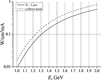
Figure 3. Calculated power of x-rays deposited on PET film vs. electron beam energy for direct x-ray beam, and after a 2 μm thick titanium membrane serving as x-ray mask support.
Download figure:
Standard image High-resolution imageIn particular, the contrast of the x-ray mask decreases with increasing electron beam energy, as shown in figure 4. It should also be noted that without sample scanning, the mask contrast depends on the distance from the median plane according to the angular distribution of the x-ray spectrum.
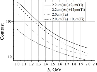
Figure 4. Calculated contrast of x-ray mask vs electron beam energy for an absorber made of gold and tantalum on titanium membranes of different thickness, averaged over a spectrum of deposited radiation (in case of mask/sample scanning).
Download figure:
Standard image High-resolution imageIn the case of a thick material layer, which is the main point of deep x-ray lithography, minimization of lateral etching requires the maximum possible contrast [40]. Moreover, in order to achieve the maximum contrast, it is important to increase both the contrast of the resist and the contrast of the x-ray mask itself, which together affect the spatial resolution during image transfer [40]. Desta and Göttert theoretically studied the effect of the x-ray mask contrast and the capabilities of manufacturing technology; they estimated the optimal value of the x-ray mask contrast that satisfies the requirement of size transfer accuracy at approximately 30 [41].
The variation of the local exposure of the substrate behind a pore depends on many parameters, namely the spectrum of the absorbed radiation, the thickness and material of the mask membrane, the proximity gap between the mask and the substrate, the size of the x-ray source, and the distance to it. To avoid ambiguity when characterizing a mask, we defined its contrast as the relative transmission, which is given only by the thickness and materials of the mask. Additionally, the resulting distribution of exposure on the substrate is given by considering the above parameters.
2.2.3. Thermal expansion of x-ray mask.
Another factor that limits the patterning accuracy is the thermal expansion of the x-ray mask. Because of the low transparency of the x-ray mask, a significant portion of the x-ray power is absorbed by the x-ray mask. The pattern distortion caused by the non-parallelism of the incident x-ray beam can be used as a critical value of the thermal expansion. For an x-ray mask of 60 mm in size (which is typical for x-ray lithography), the estimated projected distortion is 0.2 μm at the 0.1 mm gap between the mask and substrate. However, the thermal expansion of the x-ray mask exceeds the estimated limit for the selected energy range, as shown in figure 5. Nevertheless, the thermal expansion can be reduced either via sectional irradiation with alternating irradiated and non-irradiated areas, or by using a rib-supported mask. Then, the non-irradiated areas will prevent expansion of the large-area mask.

Figure 5. Calculated thermal expansion of 60 mm x-ray mask in horizontal direction (in mask plane) vs electron beam energy for electron beam current of 70 mA for evacuated chamber.
Download figure:
Standard image High-resolution imageThe temperature trend during the exposure process is explained above. In addition to the approximate estimate proposed, the temperatures of the x-ray mask and film fixed to a cooled substrate were calculated using the heat conductivity equation, as previously demonstrated [42–44]. For an average electron current of 70 mA in the synchrotron source at an electron energy of 1.2 GeV, a helium pressure in the exposure chamber of 80 mTorr, a proximity of 350 µm, a scanning speed of 20 mm s−1, and a scanning amplitude of 30 mm, the overheating of the x-ray mask with a diameter of 25 mm was approximately 1° relative to the substrate.
3. Discussion
3.1. x-ray power density
As shown in section 2.2.3, thermal distortion can be suppressed for a lower electron beam energy. However, such exposure condition results in dramatically increased exposure duration to achieve the required high dose [30]. Therefore, power density augmentation in the irradiated area is an important task. But, owing to the diffraction of x-rays by features of x-ray mask patterns, constructive interference occurs behind the x-ray mask, at a distance depending on the feature size [45]. This is possible because of the coherent illumination of the features, whose size is, by order of magnitude, approximately equal to the transversal coherency area. Figure 6 shows the interference patterns for different conditions, as calculated for the x-ray spectrum at the LIGA beamline for E = 1.2 GeV and exposure It = 8500 mA min, where I is the electron beam current and t is the exposure duration. In this case, the area with the significantly increased intensity is substantially smaller than the opening in the tantalum x-ray mask. As indicated by the simulation, the phase shift by the x-ray mask membrane plays an important role as the x-ray mask is partially transparent to radiation containing a hard spectrum component.

Figure 6. Calculated x-ray interference patterns in several proximity gaps behind the x-ray mask containing openings of 0.5 µm in diameter in the membrane. The x-ray mask is a 2 μm thick tantalum membrane.
Download figure:
Standard image High-resolution imageThus, when the features of the x-ray mask are small enough, it is possible to achieve higher throughput by tuning the beamline setup for the task of pattern miniaturization.
Additionally, the use of hard x-rays in x-ray lithography provides a unique opportunity to create structures extended in the direction of SR beam propagation. The image of an x-ray mask can be simultaneously transferred into several layers of the polymer film, stacked over one another; the substrate films were fixed to one another by electrostatic forces, as well as mechanically, along the perimeter of the substrate. When patterning on a thick layer, the variation in the dose across the thickness of the material varies from two- to four-fold, which leads to an increase in the sidewall inclination owing to the different rates of lateral under-etching. However, for films packed in a stack, the variation in the dose between the films is relatively low, as shown in figure 6. Furthermore, compared with patterning a single thick layer (where the solvent attacks the thick pattern from one side), the duration of individual post-exposure processing of the thin films was substantially less.
3.2. Etching optimization
In manufacturing high-aspect-ratio microstructures, it is necessary to minimize the lateral etching rate. However, as wet etching rate is isotropic, it can be controlled with the deposited dose distribution. Therefore, it is necessary to determine the conditions under which the maximum etching contrast in the course of wet etching is realized. But, under normal conditions, the etching contrast changes non-monotonically [30]. For this reason, the etching rate and etching contrast were studied against the x-ray deposited dose using megasonic agitation with a frequency of 1 MHz. A 250 W SONOSYS generator was used. Figure 7 shows the measured non-monotonic dependence of the etching rate on the alkaline concentration, which is defined by the PET fragment hydration process.
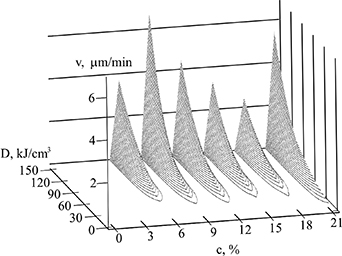
Figure 7. Measured etching rate for exposed PET vs alkaline concentration for different x-ray doses and for megasonic bath at 40 °C.
Download figure:
Standard image High-resolution imageThe polymer etching contrast derived from figure 7 is shown in table 2. When the dose exceeds 80 kJ cm−3, the etching rate deviates slightly from the power law, which is typical for low doses and can be interpolated by the exponential factor exp (−D/Dm), where Dm = 3000 kJ cm−3.
Table 2. Measured etching rate v and etching contrast s of PET for different alkaline concentrations and different x-ray doses. Agitation frequency 1 MHz. Bath temperature 40 °C. v(D, c)(μm min−1) = q + u {D(kJ cm−3)exp(–D/Dm)}s.
| Deposited dose (kJ cm−3) | |||||||
|---|---|---|---|---|---|---|---|
| 0–42 | 42–92 | 92–250 | |||||
| Alkali concentration, c | q | u | s | u | s | u | s |
| 6 | 1.1 × 10⁻³ | 1.2 × 10⁻⁵ | 2.68 | 6.7 × 10⁻⁷ | 3.46 | 1.1 × 10⁻⁴ | 2.34 |
| 9 | 2.9 × 10⁻³ | 2.5 × 10⁻⁴ | 2.06 | 3.3 × 10⁻⁵ | 2.59 | 9.5 × 10⁻⁸ | 3.87 |
| 12 | 4.5 × 10⁻³ | 5.5 × 10⁻⁴ | 1.88 | 7.0 × 10⁻⁵ | 2.41 | 7.9 × 10⁻⁶ | 2.91 |
| 15 | 8.3 × 10⁻³ | 5.8 × 10⁻⁴ | 1.72 | 7.5 × 10⁻⁵ | 2.30 | 3.7 × 10⁻⁶ | 3.00 |
| 18 | 7.5 × 10⁻³ | 2.9 × 10⁻³ | 1.30 | 7.0 × 10⁻⁵ | 2.30 | 1.2 × 10⁻⁵ | 2.70 |
| 21 | 1.2 × 10⁻² | 3.5 × 10⁻² | 1.00 | 4.6 × 10⁻³ | 1.55 | 9.0 × 10⁻⁶ | 2.92 |
This fact is most important at high doses, where competing processes such as destruction and crosslinking reaction are observed [46].
Nevertheless, despite the high etching rate, the sidewall inclination increased slowly with dose. On the other hand, the sidewall inclination depends not only on the material etching rate, but also on the removal rate of destroyed products from micropores, which depends on their diffusivity [47]. To use the model correctly, it is necessary to determine the diffusivity for the actual temperature and alkali concentration.
Table 2 shows that varying the alkaline concentration and the dose of absorbed radiation can provide a wide range of etching rates, from a few nanometers to a few micrometers per minute, which enables optimization of the etching process.
3.3. Pore etching model
Based on the results of the etching rate measurement given in table 2, the profile of micropores we calculated using modeling for different etching conditions and exposure variation. Specifically, x-rays irradiate the polymeric material through the hole in the membrane of the x-ray mask, which is located 350 µm from the substrate made of PET.
For pores less than 2 μm in diameter, the steady motion in the pore cavity is strongly suppressed, as follows from the low values of the Peclet and Sherwood numbers. At the same time, at high values of the diffusivity, the influence of the pore depth, which is less than several centimeters, on the mass transfer of the etching products from the pore and from the influx of fresh portions of the etching agent can be neglected [47]. Then, the lateral etching rate v(r) in the pore area was calculated as
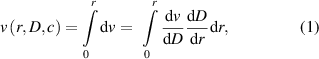
where r is the distance from the center of the irradiated region. Substituting the dependencies v(D) and D(r) into equation(1) yields

where the parameters q, s, and u are functions of the alkali concentration, which are presented in table 2.
It is convenient to divide the pore-creation process into two stages. In the first stage, the pore is etched from two sides of the film to form an infinitely thin bridge. In the second stage, the bridge is broken, and the pore walls are smoothed because of the higher etching rate at the pore axis.
Figure 8 shows the pore profiles at various etching times. It can be seen that after the bridge was etched away, the pore diameter increased slightly, the side wall was substantially smoothed. On this basis, it is convenient to compare the pore profiles in the first stage of etching. For this reason, the pore depth vs the pore radius for different doses and alkali concentrations is displayed in figure 9. The abscissa is the distance from the pore axis, and the ordinate is the pore depth.

Figure 8. Calculated pore profiles every 2 min of etching, for c = 6% and D = 60 kJ cm−3. The etching parameters were taken from table 2.
Download figure:
Standard image High-resolution image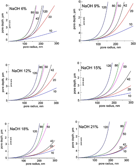
Figure 9. Calculated pore profiles at different concentrations and doses (kJ cm−3) of deposited radiation after the first etching stage. The calculated etching rate was obtained using the data given in table 2. The difference in the etching depth on the front side and backside of the pore does not exceed 0.2 µm and is not shown in the figure.
Download figure:
Standard image High-resolution imageAs shown in the figure, pores with a diameter below 400 nm can be obtained when the dose exceeds the value of 80 kJ cm−3, regardless of the etching contrast value. At the same time, as the alkaline solution concentration increases, the slope angle of the pore walls relative to the film plane decreases, and thus the optimal etching conditions correspond to a low solution concentration.
3.4. Experimental verification of the proposed optimization
An array of micropores was manufactured by irradiating a 10 μm thick PET film through an x-ray mask containing round openings in the tantalum membrane as the absorber. The deposited radiation dose was approximately 70 kJ cm−3 for E = 1.2 GeV. Afterward, the irradiated films were etched in a custom alkaline water solution containing six parts anhydrous NaOH dissolved in 100 parts deionized water (by weight).
The irradiated PET films were etched in an electrolytic cell (figure 10) at 40 °C under megasonic agitation. The etching process was stopped as soon as the cell resistance decreased to a minimum value. The voltage drop within 1 min indicates a high uniformity of the etching process. The resulting micropore array is illustrated in figure 11.

Figure 10. Photograph of the electrolytic cell used for etching.
Download figure:
Standard image High-resolution image
Figure 11. Scanning electron microscopy images of areas of the etched PET film (a)–(c) and x-ray mask (d).
Download figure:
Standard image High-resolution image
Figure 11 represents an area of the film with pores produced under different conditions: exposure to a deposited dose of 60 kJ cm−3 followed by (a) etching in a 21% NaOH solution for 40 min; (b) etching in a 6% NaOH solution for 30 min; (c) etching in a 6% NaOH solution for 15 min. Etching was performed at 40 °C.
As seen from figures 11(а) and (b), the pores were etched through, and the channels had a cylindrical shape, the diameter of the channels was approximately 1500 nm and 500 nm with an aspect ratio of approximately 7 and 20, respectively. In figures 11(a) and (b), the side walls of the channels have a shape close to cylindrical. The pores in figure 11(b) look curved due to the expansion of the film when it is broken, since the film remains rigid despite the pores with submicrometer pore diameter.
The small deepening around the pore in figure 6 was caused by a halo in the intensity around the center of the irradiated area (see figure 6), where the pore diameter was significantly lower than that of the original one in the x-ray mask (shown in figure 11(d)).
The proposed technique may be applied in the manufacturing of microcomponents for micromechanics, microoptics, microfluidics, etc. It should be noted that x-ray power optimization is especially important for the treatment of fluoroplastic materials, which are characterized by the threshold power of deposited radiation [48].
A large number of SR sources can be used for microstructuring; however, these are not implemented in practice because the optimal conditions for the process have yet to be established. However, tuning the spectrum to the manufacturing process conditions is possible using x-ray mirrors or a central beam-stop, as shown by Nazmov et al [42].
4. Conclusions
In this work, the optimal energy of the SR source for special micromachining was determined, which could provide high-contrast x-ray masks during patterning on a thick PET layer with tolerance in the nanometer range. Radiation-induced transformation of PET molecules include both destruction and cross-linking of in-situ fragmented molecules, which affect the monotonous etching rate function of the deposited x-ray dose. A deposited radiation dose of approximately 70 kJ cm−3 was found to be sufficient to achieve an etching rate of approximately 420 nm min−1, and a microstructure aspect ratio of at least 20.
Acknowledgments
The part relating to microstructuring was performed at the shared Siberian Synchrotron and Terahertz Radiation Center (CU SSTRC) on the basis of the VEPP-4—VEPP-2000 complex at BINP SB RAS, using equipment supported by the Ministry of Education and Science of the Russian Federation Project Number RFMEFI62119X0022. The study of regular membranes in this work was supported by the Ministry of Education and Science as research under RFBR Grant Number 18-29-20090. This work was also supported in part by the Ministry of Education and Science of the Russian Federation Grant Number АААА-А19-119062690004-0. This work was also supported by the Ministry of Science and Education as part of work under the State Assignment FSRC «Crystallography and Photonics» Russian Academy of Science in part of electron microscopy of specimens.
Data availability statement
All data that support the findings of this study are included within the article (and any supplementary files).
Author contributions
V N: methodology, investigation, writing—reviewing and editing. B G: data curation, Software. A V: conceptualization, visualization. V A: funding acquisition, project administration, supervision.