

Abstract
In this paper, the fabrication of plastic microfluidic circuits using integrated electrothermal actuators is described. The materials used to do this task are aluminium, biocompatible glue and polymethylmethacrylate (PMMA). These materials are processed to integrate electrothermal actuators on transparent and biocompatible PCB-like substrates. The actuators reach a temperature between the glass transition temperature and the melting point of the PMMA in order to perform the bonding. The PCB-like substrate allows the integration of additional circuitry if required. The proposed method of fabrication guarantees transparent devices. To do this task, the facilities are not expensive, and allow industrial production because many devices can be assembled at the same time. Finally, the proposed method is checked. In order to do so, a T-junction microfluidic circuit for bubbles generation is fabricated. The microchannels have a width of  m and a height of
  m. The generation of bubbles was tested with successful results and good correspondence with the theoretical behaviour. Leakages were not observed during experiments, demonstrating the feasibility of the bonding method for fabricating microfluidic devices using thermoplastics materials.
Export citation and abstract BibTeX RIS
1. Introduction
Nowadays the microfluidic devices field is the center of attention of many research areas. The synergy of microfluidic circuits and a specific research area means a multidisciplinary field which provides useful solutions for many problems. For instance, the developments of lab on chip (LOC) devices reported on [1–3] are very representative examples. Generally, the microfluidic devices have to fulfil many demanding requirements, for example, transparency and biocompatibility.
The LOC devices fabricated using printed circuit board (PCB) substrates are named lab-on-PCB (LOP) devices. The development of these devices is very incipient, and their market introduction is being carried out using commercial PCBs [4]. However, many often, the development of microfluidic devices using commercial PCBs is not optimal. The main drawbacks are the lack of biocompatibilty due to the use of copper, and their opacity for optical applications. Regarding the fabrication, the most important difficulty is the assembly of the PCB substrate with a cover to achieve buried microchannels and chambers. There are several method to do so, for example, the use of double side tapes [5–7] or glue [8, 9]. Regarding the biocompatibility, transparency and low cost, a combination of polymethylmethacrylate (PMMA) and aluminium has been reported as PCB-like substrate [9]. This transparent and biocompatible substrate represents the link between PCBs and the most commonly used materials for microfluidic fabrication, that is, polymethylmethacrylate, polycarbonate (PC), polyethylene terephthalate (PET) and cyclic olefin copolymer (COC) [10]. In this case, the bonding of different parts of the device is solved [10, 11]. Typically, this bonding is carried out by using the material itself, that is, PC to PC [12], PMMA to PMMA [13–15], or COC to COC [16]. Although these methods are useful for rapid prototyping, their potential for mass production is low. This is because the required surface modification of the materials is performed using vapours of solvents such as ethanol, isopropyl alcohol, ethyl alcohol or acetone. From our point of view, the method reported on [17] is a very interesting procedure for fabricating plastic microfluidic circuits without using vapours of solvents. This method uses gold microwave susceptors. This increases the cost of the device due to use of gold, and decreases the transparency. Finally, different materials can be bonded, for example polyether ether ketone (PEEK) to polystyrene (PS) [18]. This last method also uses surface treatment of the plastic, in this case, using plasma.
In this paper, a method for fabricating PMMA microfluidic circuits using integrated electrothermal actuators is proposed. The materials proposed for the method are transparent and biocompatible. The actuators reach a temperature close to the melting point of the PMMA. The proposed procedure of fabrication assures the fabrication of transparent devices. In order to do so, the required facilities are not expensive and the surface treatment of the plastics is not necessary. Finally, as a proof of concept, the proposed method is used for fabricating a T-junction microfluidic circuit for droplet generation.
2. Bonding process
In this section, the principle of working of the proposed bonding method (PMMA to PMMA) is described. The main idea of the method consists in bonding the PMMA walls of a device with a PMMA substrate in order to fabricated buried microchannels. The bonding is performed when the glass transition temperature is slightly exceeded.
In order to explain the process in detail, an example of a simple structure is chosen, figure 1. In figures 1(a) and (b) both the top and cross-sectional views of the PMMA structures before bonding can be seen. The bottom PMMA is a PCB-like substrate with an aluminium line acting as a heater. The heater is used for increasing the temperature of both the bottom part of the PMMA walls and the corresponding area of the PMMA substrate. In order to do so, the heater is fabricated over the PMMA substrate being its geometry similar to the PMMA walls. The heating is performed by Joule effect, so that, an electrical current is applied to the pads of the heater. In addition, the heater has to be designed to have a homogeneous temperature in the whole geometry so that the bonding is performed in the completed geometry at a time. This characteristic is achieved thanks to COMSOL simulations, where the maximum and minimum reached temperatures can be studied as a function of the widths of the heater lines. The simulated model includes the top PMMA, the bottom PMMA with the aluminium line and the surrounding air. The simulations and experimental results performed for this method provide a maximum increase of temperature of ( C) for a good bonding. If the increase of temperature is higher than (
 C), parts of the device could start to boil if the heating time is increased. Meanwhile, other parts have not been bonded. This effect was confirmed by experiments.
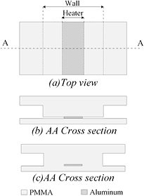
Figure 1. (a) The top view and (b) cross sectional view of the simplest structure before bonding can be seen. (c) The parts after bonding are shown.
Download figure:
Standard image High-resolution imageBriefly, the PMMA wall is placed over the aluminium heater, as can be seen in figures 1(a) and (b). Once the wall and the heater are aligned, a pressure is exerted. After that, an electrical current is applied to the pads of the heater. It is important to comment that the PMMA and the aluminium have very low adherence, and leakages between them could appear. In order to solve this problem, the aluminium line has to be embedded on the PMMA wall. The two PMMA surfaces start to bond when the temperature exceeds the glass transition temperature of the PMMA ( C) and reaches about (
 C) around the heater, particularly just in the PMMA surfaces below and above the heater, resulting in a single piece after the bonding, figure 1(c).
It is important to highlight that the cooling down has to be controlled in order to avoid both the debonding and the thermal stresses, that is, the decrease of temperature has not to be abrupt. In order to do so, the decrease of temperature is performed reducing the current 200 mA every 2 min. During this time, the pressure has to be applied. We recommend reaching ambient temperature using this procedure. However, theoretically, the maximum temperature to finish the cooling down without debonding could be slightly lower than the glass transition temperature, but thermal stresses could appear when the ambient temperature is reached.
The geometry presented in this section is the simplest one. However, this method can be extended to more complex geometries, as will be demonstrated in the following section, section 3.
3. Design and simulations
In order to check the feasibility and reliability of the proposed bonding process, a device for generating bubbles is fabricated. This device is going to be fabricated following the aforementioned bonding method. A sketch of the microfluidic circuit is shown in figure 2, where w is the width of the channels. The chosen device is a T-junction bubble generator because it is well-known in the microfluidic field. This allows the validation of the proposed bonding method using a friendly application.

Figure 2. Geometry of the T-junction microfluidic device.
Download figure:
Standard image High-resolution imageAs can be seen, the device has two inlets, I1 and I2, for the dispersed (air) and carrier fluids (liquid) respectively, and a output O. The equation which governs the length of the bubble L is reported on [19].
Where QI1 and QI2 are the flow rates of the dispersed and carrier fluids respectively, and α is d/w. Where d is the value of the neck of the bubbles before breaking, and w is the width of the microchannel [19].
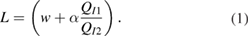
Taking into account the dimensions of the device, the geometry used for designing the actuator (heater) can be seen in figure 3(a). The actuator aligned with the microfluidic circuit are shown in figure 3(b). This geometry is included in the model of the COMSOL to perform the simulations. The materials used are aluminium for the metallic lines, PMMA for the substrate, micromachined PMMA as cover, and air on the rest of the boundaries. The previously mentioned materials are included in the COMSOL materials library. The boundary conditions, are all of them, convection with air. The convection is modelled using the correlations included in COMSOL which compute the heat transfer coefficient. Finally, the applied current to the actuator is  A.
A.
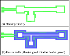
Figure 3. (a) Geometry of the heater obtained using the COMSOL simulations, and (b) the heater and the microfluidic circuit are depicted.
Download figure:
Standard image High-resolution imageThe simulation are performed using two 2 mm-thick PMMA sheets. One of them is used for defining the microchannels and walls, where the microchannels have rectangular shape with a width of  m and a height of
  m. The aluminium lines have a height of 20 μm. The rest of the dimensions of these metallic lines has to be obtained by simulations to reach the homogeneous distribution of temperature.
The results of the simulations are shown in figure 4. The distribution of temperature around the aluminium lines can be seen in figure 4(a), and the experimental thermal image of the device during the fabrication is shown in figure 4(b). As can be seen, the field of temperature of the simulations corresponds to the experimental results.

Figure 4. (a) The distribution of temperature around the aluminium lines can be seen, (b) experimental thermal image of the device during the fabrication.
Download figure:
Standard image High-resolution imageIn addition, the temperature as a function of the time is depicted in figure 5. The simulation result corresponds to the optimized design for an minimum increase of temperature of  C.
C.

Figure 5. The simulated temperature as a function of the time is depicted.
Download figure:
Standard image High-resolution imageThe time necessary for performing the bonding, in this particular case, is 180 s. The parameters obtained as a result of the simulations are used for fabricating the device.
4. Fabrication results
The process starts with two 2 mm-thick PMMA sheets. The first PMMA sheet is milled following the shape and dimensions previously commented. The height of the milling is  m for the microchannels, and
  m for the rest of the PMMA. The second PMMA sheet is laminated with an aluminium sheet of
  m using the method reported on [9]. After that, the aluminium tracks defined in section 3 are fabricated using wet etching. In this last step, the heater is fabricated, being 2 Ω its resistance at room temperature. Then, the PMMA parts are manually aligned using a microscope. Finally, the bonding is performed using the parameters obtained in section 3, that is, a current of 2.5 A during a time of 180 s. The bonding force is applied by using two spring clamps (force = 6.2 Kg). The total area which supports that force is the area of PMMA walls (blue color in figure 3). The value of this area is
  . Therefore, the applied pressure is
  , that is,
  . The two parts of the fabricated device are shown in figures 6(a) and (b). The fabricated device can be seen in figure 6(c).
Figure 6. (a) Bottom PMMA sheet after both lamination and wet etching, (b) top PMMA sheet after micromachining, and (c) fabricated device after the bonding technique.
Download figure:
Standard image High-resolution imageIt is important to highlight that the choice of the minimum width of the aluminium line is fixed to  m. The reason to do that, is to reduce the fabrication tolerance of the aluminium lines due to the under etching. This value is about
  m resulting an error of about 4%.
A sketch of the cross-sectional view of a microchannel before bonding figure 7(a) and after bonding figure 7(b) are shown. As can be seen in figure 7(c), there is not border between the PMMA bonded parts.
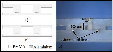
Figure 7. (a) Sketch of the cross-sectional view of the device before bonding, (b) the same structure after bonding, and (c) cross-sectional view of the result of fabrication.
Download figure:
Standard image High-resolution image5. Experimental results
This section shows the experimental results of the T-juntion device for bubbles generation. To do this task, different values of QI1 and QI2 are chosen.
Two immiscible fluids are used for the generation of bubbles. In particular, air and coloured water are used as dispersed and carrier liquids, respectively, figure 8. The flow rate QI1 ranges between 15 μl s−1 and 250 μl s−1, and QI2 ranges between 50 μl s−1 and 150 μl s−1. In figure 8, the beginning of the bubble creation can be seen. Figure 8(b) shows the bubble generation for QI1 = 150 μl s−1 and QI2 = 100 μl s−1 where the L is 4.2 mm and the length of the liquid phase is 2.8 mm.

Figure 8. (a) Beginning of the bubble generation and (b) generated bubbles for QI1 = 150 μl s−1 and QI2 = 100 μl s−1 are shown.
Download figure:
Standard image High-resolution imageFollowing the procedure of [19] for representing the experimental results, the fitting curve and the experimental points can be seen in figure 9. The x-axis and y-axis are  and the
  , respectively. For the fabricated device, the value of d is about 1 mm. The fitting has a squared correlation coefficient R2 = 0.9913, demonstrating a good correspondence between the experiment and the theory.

Figure 9. Fitting curve and the experimental points of the bubbles generation.
Download figure:
Standard image High-resolution image
The most important conclusions obtained from the experiments are the absence of both significant deformations of the microchannels and leakages, demonstrating the feasibility of the bonding method for fabricating microfluidic devices using thermoplastics materials. In addition, the contact between the working fluids and the aluminium is avoided due to the metal is embedded in the thermoplastic.
Theoretically, the procedure can be applied to smaller microchannels as long as COMSOL simulations provide a good result. However, the precision of the current, time, and specially the applied pressure have to be carefully studied. In addition, the proposed procedure of bonding based on COMSOL simulations can be developed for complex structures as long as the maximum increase of temperature between points of the heater is guaranteed.
6. Conclusions
A method for bonding the thermoplastic parts of microfluidic circuits has been described. The main characteristics of the method are biocompatibility, transparency and mass production fabrication. The biocompatibility is due to the used materials such as PMMA and aluminium. Other plastic and metallic materials can be used if a new fabrication parameters are chosen. The transparency is achieved thanks to the use of the mentioned PMMA, but PC, COC, PET and polyestyrene (PS) could be used to fulfil the same requirement. The mass production characteristic is due to the used materials and facilities, all of them with a low cost. More importantly, the nature of the method allows the fabrication of many devices at a time, using a parallel configuration of actuators to be simultaneously actuated. Moreover, the method does not need the use of vapours of solvent to modify the surface characteristics of the plastics.
The aluminium is used for fabricating the electrothermal actuators. These devices increase the temperature of the PMMA walls in order to perform the bonding. The dimensions of the electrothermal actuators are obtained by numerical simulations with good agreement with the experimental results. Moreover, the simulation of more complex thermal actuators geometries is possible.
The proposed method of bonding is used to fabricate a T-junction bubble generator. The results of the fabrication are good, with no leakages nor deformations; and bubbles have successfully been generated. Finally, the theoretical behavior of the bubble generator fits the theory. All these comments demonstrate the feasibility of the method to build biocompatible and transparent microfluidic circuits.
Acknowledgment
This work was supported by the Spanish Ministry of Science and Innovation (project TEC2014-54449-C3-2-R, BIOLOP).