
Abstract
To achieve the expected level of sensitivity of third-generation gravitational-wave (GW) observatories, more accurate and sensitive instruments than those of the second generation must be used to reduce all sources of noises. Amongst them, one of the most relevant is seismic noise, which will require the development of a better isolation system, especially at low frequencies (below 10 Hz), the operation of large cryogenic silicon mirrors, and the improvement of optical wavelength readouts. In this framework, this article presents the activities of the E-TEST (Einstein Telescope Euregio Meuse-Rhine Site & Technology) to develop and test new key technologies for the next generation of GW observatories. A compact isolator system for a large silicon mirror (100 kg) at low frequency ( 10 Hz) is proposed. The design of the isolator allows the overall height of the isolation system to be significantly compact and also suppresses seismic noise at low frequencies. To minimize the effect of thermal noise, the isolation system is provided with a 100 kg silicon mirror which is suspended in a vacuum chamber at cryogenic temperature (25–40 K). To achieve this temperature without inducing vibrations to the mirror, a radiation-based cooling strategy is employed. In addition, cryogenic sensors and electronics are being developed as part of the E-TEST to detect vibrational motion in the penultimate cryogenic stage. Since the commonly used silicon material is not transparent below the wavelengths typically used in the 1 µm range for GW detectors, new optical components and lasers must be developed in the range above 1500 nm to reduce absorption and scattering losses. Therefore, solid-state and fiber lasers with a wavelength of 2090 nm, matching high-efficiency photodiodes, and low-noise crystalline coatings are being developed. Accordingly, the key technologies provided by E-TEST serve crucially to reduce the limitations of the current generation of GW observatories and to determine the technical design for the next generation.
Export citation and abstract BibTeX RIS

Original content from this work may be used under the terms of the Creative Commons Attribution 4.0 license. Any further distribution of this work must maintain attribution to the author(s) and the title of the work, journal citation and DOI.
1. Introduction
Since Albert Einstein's prediction of the existence of gravitational waves (GWs) in 1915, several GW observational campaigns have been conducted around the world. These activities were crowned with success when GWs were successfully detected by the US-based detector LIGO (Laser Interferometer Gravitational-wave Observatory) on 14 September 2015 [1, 2]. The experiments carried on over the year to improve the sensitivity of the instruments hold great potential for the development of a more accurate measurement system, as shown by the improvements in the isolation system of LIGO, which achieved isolation in the amplitude of about a factor 300 at 1 Hz and about 3000 at 10 Hz [3]. Further evidence is provided by experimental results from the Superattenuator at Virgo, which shows the isolation of about ten orders of magnitude at 10 Hz [4].
To date, many GW measurement systems are being built around the world to detect these waves with an exceptionally accurate laser interferometer detector [5–8]. For example, five large ground-based GW telescopes with a large laser interferometer detector are currently in use [9]: the two Advanced LIGOs in the USA [6], completed around 2015, GEO 600 in Germany [7, 10], completed around 2016, Advanced Virgo in Italy, completed in 2017 [5], and KAGRA (Kamioka Gravitational Wave Detector) in Japan, completed in 2020 [8]. These telescopes (except GEO 600) are called second-generation telescopes because they are the improved versions of the first-generation telescopes: LIGO [11], VIRGO [12], and TAMA300 [13]. The second-generation telescopes run with about one order of magnitude better sensitivity than the first-generation telescopes, being sensitive in the frequency range 10–2000 Hz. [8]. This means that the observable volume is 1000 times larger. Alternatively, the Einstein telescope (ET) [14] and the Cosmic Explorer (CE) [15] are considered third-generation GW observatories that are expected to achieve one order of magnitude better performance in sensitivity than the second-generation telescopes [16]. To achieve this goal, the frequency range of detection must be broaden below 10 Hz. This will allow the detector to be sensitive to objects emitting GWs at frequencies below 10 Hz, where instruments are currently blind, enabling the study of sources whose physical structure and astrophysical features are still unknown, and also the study of the features of a wave in the earlier phases of the inspiral, in the case of binaries [17]. This last point is crucial for the development of multi-messenger astronomy involving electro-magnetic detectors (EM), where the longer the observing time, the better the communication between GW and EM instruments [18]. Another important consequence is that if the instrument could detect in a broader range of lower frequencies, it is possible to identify objects that are at higher redshifts, i.e. more ancient, or apparent high masses that are increased by a cosmological distance [19]. Examples of these objects are intermediate mass black holes or stellar-mass black holes (BHs), whose nature and physics are still unknown. Reducing the main sources of noise (such as seismic noise, thermal noise, quantum noise, control noise, Newtonian noise, suspension thermal noise, coating and Brownian noise, and scattered noise) is then crucial and breakthrough technologies must be developed.
The approach proposed for ET and CE is very different from the currently used GW detectors. It needs to be much more sensitive at low frequencies, which requires better isolation of the mirror from seismic motions and gravity fluctuations. Another feature of the third-generation detectors is the optics. Advanced Virgo and Advanced LIGO use fused silica mirrors, which have a limited size at room temperature, and use a laser wavelength of 1064 nm [20]. KAGRA (sometimes called the Generation 2.5 detector) uses cryogenic sapphire mirrors that allow it to stay at a laser wavelength of 1064 nm [21–23]. In contrast, both ET and CE plan to operate large cryogenic silicon mirrors. Since silicon is not transparent at 1064 nm, wavelengths further in the infrared must be used, for example from approximately 1550 nm to 2100 nm [14, 15]. Several prototypes and facilities are currently being built around the world to prepare and validate the technology required for these future instruments. For ET, four research facilities are currently operated in Europe to develop all the necessary technologies required to achieve the desired performance of the ET detector: E-TEST, ETpathfinder, Amaldi Research Center (ARC), and SarGrav [24]. This article presents the current research activities of the E-TEST. These activities include the design of a compact isolation system for a large mirror (section 2), the radiative cooling of the mirror (section 3), the design of the prototype (section 4 ), and the development of the cryogenic sensors (section 5). In addition, sections 6 and 7 present the low-noise optics research activities and the proposed validation techniques, respectively. Finally, section 8 contains the conclusion [25].
2. Compact isolation for large mirror
The ET concept report published in 2011 proposed the ET isolation system, which uses a combination of passive isolators [26]. It consists of an inverted pendulum platform (IPP) and multiple cascaded pendulums. The ET isolation system is inspired by the Virgo isolation system (Superattenuator), but with an improved model to achieve the desired sensitivity requirement of ET (desired crossover frequency between the horizontal transfer function and the ET requirements (10−9) is around 1.8 Hz) [4]. The result is a 17.5 m high isolation system.
The IPP offers three key advantages: (1) it provides a point positioning system to compensate for tidal drift [27, 28], (2) it reduces the oscillation modes by providing a suitable positioning of the entire isolation system, and (3) it results in a very low horizontal resonance frequency (about 40 mHz for Virgo [4] and 70 mHz for KAGRA [29]). However, the very long ET isolation system increases design complexity and infrastructure cost [24, 30].
With this in mind, there is considerable interest in the ET community to reduce the overall height of the ET isolation system while maintaining the desired performance [14, 26, 31]. Also, the possibility of achieving better isolation performance, especially at low frequencies, if other approaches are incorporated into the isolation system [31]. For example, this can be achieved by adding an active inertial platform (AP) to the isolation system, which improves the suppression of seismic noise that is below the resonance of the structure and also allows for a smaller isolation system than a purely passive isolation approach. The LIGO isolation system is an example of this approach, based on a combination of an AP and multiple cascaded pendulum masses [3]. However, the performance of this approach is limited at low frequencies where seismic noise suppression is difficult to achieve due to sensor noise, sensor coupling, and coupling due to gravity [3, 32, 33]. The performance limitation due to sensor noise can be improved by introducing better sensor sensitivity at low frequencies as presented in this [34], while sensor coupling and coupling due to gravity are still challenges for the active inertial approach. On the other hand, the LIGO isolation system requires additional means to position the entire isolation system and compensate for tidal drift [35]. This increases the complexity of the system, which is not the case when the IPP is included in the isolation system [27, 28].
The E-TEST project presents a new isolation system for a large mirror at low frequencies that combines the features of IPP and AP in one system. As a result, the E-TEST isolation system is smaller and provides better seismic noise suppression, especially at low frequencies, than the proposed ET isolation system. This new isolation system includes an AP (improves seismic noise suppression at low frequencies with a smaller isolation system), an IPP (compensates for any tidal or mirror drift and provides a low resonant frequency), and a passive cascaded pendulum mass (suppresses seismic noise at high frequencies). The E-TEST isolation system will house a 100 kg full-size silicon mirror operating at 25 K in cryogenics and a reduced number of stages with a total height of 5.5 m, as no tower with all stages is required for validation of this hybrid technology. This new approach is being pursued for a new concept investigation for the future ET. More details about the design are presented in section 4.
3. Radiative cooling of the mirror
One of the goals of E-TEST is to cool a 100 kg silicon mirror to cryogenic temperature (25 K). As explained in section 2, the mirror is suspended in order to avoid any vibration. Vibration isolation implies that suspended parts cannot have any contact with any elements external to the inverted pendulum (IP).
Cooling down without injecting noise is an important constraint, which led our research on the development of an innovative concept for contactless cooling of the mirror. This technology is based on radiative exchanges between two intertwined radiators-like structures called inner and outer cryostats. The payload was mechanically decoupled from the rest of the cryostat in order to avoid vibrations.
Figure 1 presents the scheme of the cryogenic concept developed for the E-TEST project in close collaboration with the partners of the consortium [36]. It is based on the radiative exchanges only between an inner suspended cryostat directly attached on the cold platform (CP) supporting the mirror, and an outer cryostat, in direct connection with He shrouds and pre-cooled by a LN2 shield. It is important to notice that there is no contact between the outer parts and the inner suspended ones: this design allows to reach the goal set for radiative cooling, because it provides the required temperature without injecting vibration noise through contacts between inner and outer parts.
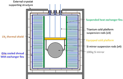
Figure 1. Design of the radiative cooling concept with its main features. The inner cryostat is in green and it is suspended because it is directly connected to the mirror to cool down. The outer cryostat is represented in blue and it is connected to helium and liquid nitrogen coolers. All the suspended elements are cooled down via an innovative contact-less procedure involving a multi-stages radiative process.
Download figure:
Standard image High-resolution imageThe required size of the radiative heat exchange area depends on two main factors: the target final temperature of the payload and the total heat load to be extracted at that temperature. A third important aspect is the transient behavior of the system: the total mass of the suspended cold elements. The cooling time should be minimized and so the mass of the cold payload (inner cryostat, mirror, CP). Assuming the total heat load to be extracted is about 0.3 W (including infrared (IR) loading through openings, harness heat leaks), the required area then depends on the emissivity at that temperature. Since the emissivity decreases drastically with temperature, even for black paint, we can assume a 0.5 emissivity. The required area significantly increases if the required target temperature is lower because it depends on the fourth power of the temperature: under these assumptions and with a sink temperature at 20 K (average temperature of the external cryostat), the required flat area of the heat exchanger is about 70 m2 for a target payload temperature of 25 K. If the external cryostat is fed with liquid helium at 4 K, this reduces to 41 m2, still for a target of 25 K.
Based on Centre Space Liege (CSL) experience on past space projects in that vacuum chamber, the FOCAL6.5 chamber provides a vacuum level about 10−6 mbar at ambient temperature. Due to the presence of the helium-cooled cryostat, vacuum level goes usually down to reach 10−7 mbar. Cryo-sorption of residual gases is not considered as an issue in the frame of the E-test project for several reasons. First, the duration of the test will be limited to 20 days, including the long cool down time. Second and most importantly, the surrounding cryostat will always be colder than the mirror and provides a much larger area ( 100× that of the mirror) to trap residual contaminant. Residual water will be first trapped by the outer layer of the cryostat cooled at liquid nitrogen. After this initial cooling, the helium cooled parts of the cryostat will then mostly trap residual nitrogen. If cryo-sorption is deemed to be an issue for future project at CSL, liquid-helium cooled charcoal panel could be used like it was used during the Planck spacecraft testing to protect the detector cooled at 0.1 K. Based on CSL experience of cryogenic tests of space instrument below 50 K, effect of cryo-sorption on the radiative cooling is not expected to affect significantly the cooling performances.
To increase the exchange area while remaining in a compact envelope, the chosen strategy is to work with a stack of horizontal fins for both cryostats: the suspended inner one and the outer one linked to the gaseous helium (GHe) fed shrouds. These fins are spaced in order to leave 2 cm gap above and bottom each fin when the inner and outer cryostats are in place (interlaced), avoiding any contact between fins and consequently cryostat structure. In order to maximize the emissivity and the cooling efficiency, the fins will be coated with thick layer of black paint on both faces. Finally, the fins are designed in order to minimize their weight while ensuring sufficient stiffness in order to keep the natural bending in the range to 1.5 mm. This intertwined radiator geometry improves the radiative exchange area by a factor of about 16 compared to the projected flat surface. This means that to reach 25 K on the inner payload with an outer cryostat at an average temperature of 20 K, the projected area can be reduced from 70 m2 to 4 m2.
4. Conceptual design of the prototype
A 3D view of the E-TEST isolation system is shown in figure 2. The isolation system consists in an active platform (AP), an IPP, a geometric-anti spring (GAS) filter, and multi-cascaded pendulum masses (Marionette (Mar) and payload). The payload contains the CP and the Mirror (Mir) which are suspended and hosted in a cryostat. These sub-isolators are further presented in this section.

Figure 2. Overview of the E-TEST prototype design. A large vacuum tank (left) hosts the cryogenic mirror suspension (right). From top to bottom we can see (1) the top GAS filter, (2) the top stage, (3) the marionette and (4) the inverted pendulum legs within pipes that support a reference ring below the top stage. The cryogenic part features (5) the inner cryostat which has the interlacing fin type heat exchanger. The whole cryostat features (6) three access points for outside experiments to interact with the cryogenic mirror. The inner cryostat is attached to (7) the cold platform. The inner cryostat fins interlace into the fins of the (8) outer cryostat which provides a cold environment and houses the (9) 100 kg silicon mirror. All of this is supported by (10) an active platform, which provides a stable and quiet environment. In turn, the active platform hangs from three large blades with have a (11) support pillar on the ground. Reproduced from [24]. CC BY 4.0.
Download figure:
Standard image High-resolution image4.1. Active inertial platform (AP)
The AP, shown in figure 3, provides inertial control in the six degrees of freedom. It is a completely redesigned and up-scaled version of the LIGO HAM-ISI (Horizontal Access Modules- Internal Seismic Isolator) platform [37] with a new diameter of 2.5 m (to host the large cryostat) and 0.75 m in height. The natural frequency of the platform AP is designed to be about 2 Hz for the vertical, pitch and roll degrees of freedom, and about 2 Hz in the horizontal and yaw (rotation about the vertical axis) degrees of freedom. This is achieved by suspending the platform using three cantilever blade springs and three flexure elements.
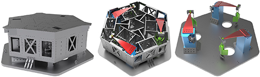
Figure 3. CAD design views of the AP (made of Aluminum). A complete view in the left, an inside view in the middle, and the flexures and blade springs are on the right.
Download figure:
Standard image High-resolution imageThe sandwich structure of the payload, made of vertical panels, is reinforced for maintaining the first flexible mode above 300 Hz. This is to guarantee high control performance in the low frequencies. The shape of this mode is further shown in figure 4 which appears at 320 Hz.

Figure 4. Different views of finite element analysis of the AP: first flexible mode appears above 300 Hz.
Download figure:
Standard image High-resolution imageParticular attention has also been paid to: (1) mass and stiffness repartition, and (2) positions of the horizontal sensors and horizontal actuators. This is to facilitate plant decoupling in view of its control.
The absolute motion of the platform is reconstructed using the signals of six inertial sensors that are embedded inside of its structure: three vertical sensors for the vertical motion (developed in the PML (Precision Mechatronics Lab) [34]) and three horizontal sensors based on Watt's Linkage (developed at KU Leuven [38–40]) for the horizontal motion. They are positioned symmetrically in a circular configuration, allowing the reconstruction of the platform's degrees of freedom. Each sensor aims for a sub-picometer resolution at frequencies below 10 Hz. This is achieved by reading the proof-mass motion of the sensor mechanics using a high resolution, homodyne, quadrature, Michelson interferometer [41, 42], which has already demonstrated 1 pm resolution above 1 Hz until the Nyquist frequency [43]. The sensor's mechanics are designed to comply with the geometrical constraints of the design and to be compatible with the ultra-high vacuum environment of the platform. The sensor's performance is expected to break through the 10−13 m/ at 1 Hz.
For inertial control, AP uses six voice coil actuators (NCCO9-39-190-1 V from H2W Technologies), three for the horizontal direction and three for the vertical direction. In addition, AP uses six BOSEMs [44] to measure the relative displacement of the platform with respect to the ground. The error signals for the controller are obtained by blending, thanks to a complementary filter the information from the displacement sensors at low frequency with the signal from the inertial sensors at high frequency.
As shown in the schematic diagram of the controller in figure 5, E-TEST applies three control loops: a damping control loop (AP damping) and an isolation control loop (AP isolation) for AP, and a damping control loop at the IPP level for the horizontal and vertical modes of the passive isolation chain. The damping control loop AP is applied to AP in the local frame, then the isolation control loop AP is applied to the same stage but in the Cartesian frame, providing inertial isolation. More details on this control strategy will be published in a follow-up article whereas a brief description can be found in [45, 46]
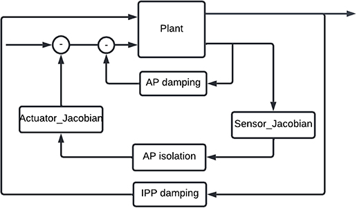
Figure 5. Schematic representation of the E-TEST control strategy. It includes three control loops. At the local frame, the AP damping is used to reduce the Q of all translational and rotational modes of the rigid body of the suspended stage. The AP isolation at the Cartesian frame can provide suppression thanks to the decoupling strategy. Finally, the IPP loop provides the final damping of the whole prototype (global control).
Download figure:
Standard image High-resolution image4.2. IP
The isolation system consists of three inverted pendulum legs (IPLs) mounted on AP that support the IPP. Each IPL, 2.7 m high, is housed in a safety tube as shown on the label No. 4 (red) in figure 2. In addition, each upper end of the IPL is attached to a 12 kg counterweight (CW) to improve the performance of the IPP. The IPLs are connected to AP and the IPP via bends of maraging steel approximately 17 mm in diameter. The diameter of the IPP is the same as that of AP and is 2.5 m. The resonant frequency of the IPP is designed to be maintained at about 70 mHz. The IPP also has three horizontal sensors and three horizontal voice coil actuators. These sensors and actuators are used for the damping loop (to damp the horizontal resonances of the IPP and the masses of the multicascaded pendulum). In addition, the IPP contains a large GAS filter.
4.3. GAS filter
The GAS filter, shown in figure 6, provides additional isolation in the vertical direction, where its suspended mode is about 250 mHz. It consists of 12 triangular blades made of steel. Each blade is 10.4 kg. The GAS filter includes a linear variable differential transformer displacement sensor and a voice coil actuator for vertical direction feedback control. Additional static positioning actuators are provided consisting of a stepper motor driven vertical correction spring and a stepper motor driven Harmonic Drive bearing for adjusting the orientation of the downstream passive filtering chain in the yaw degree of freedom. Composed of twelve springs.
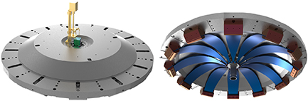
Figure 6. CAD design views of the GAS filter (top view on the left and bottom view on the right).
Download figure:
Standard image High-resolution image4.4. Marionette (Mar)
A mar, shown in figure 7 (blue), hangs from a wire (0.7 m high) at the GAS filter. It contains two stepper motors with two CWs to position the payload in angular degrees of freedom. The Mar is made of aluminum with a diameter of 0.75 m and instrumented with eight coil-magnet actuators to control the pitch, roll, and yaw degrees of freedom of the cryogenic payload (CP); error signals are provided by two built-in in-vacuum optical levers measuring the orientation of the marionette with respect to the IPP platform.

Figure 7. CAD design views of the marionette: isometric view showing the body (blue) and reference frame (left), bottom view (middle), and top view showing stepper motors and CW (right).
Download figure:
Standard image High-resolution image4.5. CP
The CP, operated at cryogenic temperature, is suspended from the marionette via three wires (1.46 m high). As shown in figure 8, the payload contains on the CP and the large mirror (Mir). The CP is a cryogenic test bed for the cryogenic sensors used to detect motion at this stage (see 5 for more details on cryogenic sensors). The Mir is suspended from the CP with four silicon rods (0.4 m high) parallel to four cantilever springs (made of CuCrZr). These cantilever springs are part of the payload, not the seismic platform. Since the silicon rods are very stiff vertically, the metal springs are used to provide some vertical compliance to suspend the mirror. This results in a 13 Hz bounce mode of the final suspension stage. The silicon mirror has a diameter of 45 cm and a total weight of 100 kg. For safety reasons, the mirror is surrounded by a cage.
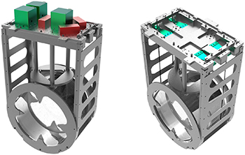
Figure 8. CAD design views of the mirror suspended from the cold platform by the silicon rods (wires shown in black) and surrounded by a safety cage. The green and red boxes (left) represent the cryogenic inertial sensors mounted on a cold platform. The cantilever blades are hidden under the cold platform and are shown in the figure on the right after the removal of the cold platform and inertial sensors.
Download figure:
Standard image High-resolution image4.6. Cryostat
As shown in figure 2 and mentioned in section 3, the cryostat is composed of two parts: the inner cryostat, suspended with the CP and the outer cryostat, including the thermal shrouds and supported by a structure placed on the optical bench of the vacuum chamber. Both cryostats are framed by interwined stack of fins, which are spaced in order to leave 2 cm gap above and below each fin when the inner and outer cryostats are in place (interlaced); this prevents any contact between fins and, consequently, the cryostat structure. In order to maximize the emissivity and the cooling efficiency, the fins must be coated with thick layer of black paint on both faces.
In order to predict the cooling efficiency of the setup, the whole cryostat was modelled with ESATAN-TMS software. The geometrical mathematical model is based on the CAD to compute the view-factors between the surfaces. One of the most critical parameter in this model is the emissivity of the black paint of the radiator fins and a worst-case approach was preferred to be conservative.
The thermal mathematical model is solved by taking into account both thermal conductivities and specific heat versus temperature. With a worst-case approach, the external cryostat assumes:
- The LN2 panels (orange in figure 9) is supporting the GHe panels, where the external fins are connected.
- The three apertures in front of the mirror are assumed to be with 30 mm diameter through the LN2 shield and GHe panels and are aligned such that only one internal fin is removed (keeping two consecutive external fins). In addition, these three holes are equipped with LN2 shield and GHe tubes in order to minimize the incoming heat load in the system (figure 9).
- The three suspension apertures are designed with 50 mm diameter on the top of the cryostat for the titanium wired and cold harness, also equipped with LN2 shield and GHe tubes protruding inside the cryostat to radiative enhance thermalization of the wires and harnesses.
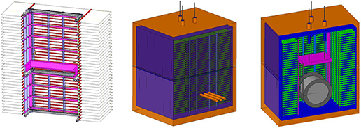
Figure 9. CAD and GMM design views of the cryostat.
Download figure:
Standard image High-resolution imageFor the inner and suspended cryostat, the design includes the following features:
- Three titanium wires coming from the marionette are assumed in Ti-6Al-4 V, an alpha-beta Titanium alloy of 4 mm of diameter.
- 20 AWG24 phosphore bronze wires for sensors.
- 10 AWG32 phosphore bronze wires for temperature sensors (cooling down monitoring).
- 4 mono-crystalline silicon rods 13 mm in diameter with thinner 3 mm diameter end sections, supporting the mirror from the CP.
- The interfaces between these sapphire rods and the CuCrZr blades of the CP are improved with indium sheets.
The biggest uncertainty in this model is the emissivity of the black paint on the radiator fins. Regarding the schedule of the project and also the available budget, we have decide to use Aeroglaze Z307 as absorptive cryogenic black paint [47, 48]. Reduction uncertainties on the black paint emissivity requires specific cryogenic test not possible in this project. Consequently, the best-case/worst-case approach based on emissivity values of the black paint gives a range of possible temperature profile for the cooling of the mirror. Figure 10 shows the results of the thermal simulation assuming that the average temperature of the outer cryostat is at 20 K and for 70 m2 of heat exchange area.
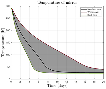
Figure 10. Temperature profiles compared with worst case and best case assumptions. The best case (green curve) corresponds to an emissivity (@ 25 (K) of the black paint of  = 0.6 which gives a stabilized temperature of the mirror of 24 K after 8.5 days (dT/dt
 1 K/day). The nominal case (blue curve) corresponds to an emissivity of the black paint of
  = 0.4 which gives stabilized temperature of the mirror of 26.74 K after 12.7 days. The worst case (red curve) corresponds to an emissivity of the black paint of
  = 0.2 which gives a stabilized temperature of the mirror of 34.8 K after 25.3 days.
Download figure:
Standard image High-resolution imageReferring to the simulation, we can predict that the mirror temperature should be between 25 K and 40 K after 20 days, under vacuum conditions. The E-TEST project will be an experimental concept validation for the pure radiative cooling down method.
It is important to note that the cooling down concept presented here can be improved in order to reach lower temperatures to meet the requirements of the experiment or application. Rooms for improvements are offered by the following:
- The He temperature at the entrance of the shrouds could be as low as 4 K improving the cooling power.
- The size of the cryostat can be adapted and consequently the heat exchange surface.
- The emissivity of the black paint can be improved (by using another paint) improving the efficiency of the cryostat as presented in this section.
5. Cryogenic sensors
E-TEST will be a testbed for cryogenic differential and inertial sensors, now and in the future. The E-TEST cryostat features many different sensor concepts and these are presented in the following subsections.
5.1. Cryogenic superconducting inertial sensors (CSISs)
For the current generation GW detectors, a monolithic Watt's linkage with an interferometric readout was developed at Nikhef between 2014 and 2018 [40]. It achieved a displacement sensitivity of 8 m/
m/ Hz from 30 Hz onwards and a modelled shot noise limited 2
 m/
m/ Hz above 10 Hz. ET will extend the detection band down to 3 Hz by, among other technologies, applying cryogenics. The current ET design features a physical link from cryocooler to the last stages of the mirror suspensions, possibly introducing unwanted vibrations near the mirror bypassing the isolation systems. The penultimate mass of the ET mirror suspensions extracts heat conductively from the 18 K mirror via its suspensions and is around 5 K.
To monitor the cryogenic penultimate stage down to 10−15 m/ Hz below 10 Hz, a new class of inertial sensors is needed. CSIS [49, 50]—an evolved design from the Nikhef accelerometer—aims to reduce its shot noise limited 10−15 m/
 Hz sensitivity down to 1 Hz by lowering the thermal noise. All other readout and actuation noise can be designed to be below the thermal noise, which itself can be lowered by the reduced temperature and increased suspension quality factor Q. The sensor self-noise features a 50-fold reduction of thermal suspension noise over the previous design by increasing the mechanical Q factor. This is achieved by using niobium instead of high-strength aluminum as mechanics material and changing the actuator from coil-magnet to superconducting coil. The permanent magnet resulted in significant eddy current damping which was a dominant (viscous) damping mechanism in the previous design, reducing the Q from about 4000 to 40 [51]. The thermal noise, which determines the sensitivity at low frequency, is proportional to
  [52] and thus, in this case, increased by a factor of 10. A schematic overview of the sensor is shown in figure 11. For a 1 kg-proof mass, the niobium Watt's linkage is
  cm3 in size.

Figure 11. A cryogenic superconducting monolithic inertial sensor. An interferometric readout provides an error signal containing information on the position of the proof mass. The proof mass is inertially suspended from the frame by a regular pendulum and inverted pendulum (a Watt's linkage) and allows for an arbitrarily low natural frequency, thereby increasing the mechanical sensitivity. The error signal is fed to the actuators to lock the mass with respect to the frame and is used as sensor output. The custom cryo-chip is under development using nanoscale CMOS technology, discussed in section 5.2.
Download figure:
Standard image High-resolution imageCSIS exploits the cryogenic temperatures by using superconducting thin film spiral coil actuators. The low-voltage superconducting coils exert magnetic pressure on the proof mass surface because of the Meissner effect. Because they are push actuators only, two actuators are needed per inertial sensor. For ET, the sensor mechanics and coils will be fabricated out of niobium. The temperature necessary for niobium, the sensor mechanics material, to be in a full Meissner state is about 5 K. The penultimate mass at around 5 K is therefore a suitable place to use the sensor for monitoring the effect of the low-vibration cryogenic systems and possibly contribute to the suspension control. The absence of magnets ensures that the suspension is structurally damped and we assume a Q factor of 104. The noise budget in figure 12 shows the expected performance of the CSIS compared to the state-of-the-art, defined here as the most sensitive inertial sensor found in the GW field that is used in suspensions and on the market. At 1 Hz, the sensitivity is more than three orders of magnitude higher.

Figure 12. Minimum detectable inertial displacement for a cryogenic, structurally damped accelerometer with interferometric readout and superconducting coil actuators with a suspension resonance frequency of 0.2 Hz. It is compared to two state-of-the-art inertial sensors (the T360, [53] and AEI;s accelerometer [54]).
Download figure:
Standard image High-resolution imageProgress on the superconducting actuators is summarized in [55], where x-ray diffraction (XRD) measurements show that the right crystallographic phase for superconducting coils can be deposited. If fitted with higher  superconducting coil and proof mass surface, the inertial sensor can operate at a temperature higher than 5 K. The CP temperature of the E-TEST prototype operates at 25 K and therefore we aim to use MgB2 as superconductor. For E-TEST, we plan to install 3 CSISs on the CP exploiting the low-vibration cryogenic environment to perform a self-noise measurement using a huddle test [56].
5.2. Nanoscale complementary metal-oxide-semiconductor (CMOS) cryochip development
In order to take full advantage of the inertial sensor performance and ensure its reliability at cryogenic temperature, the electronic part of CSIS will include a fully-custom chip fabricated in nanoscale CMOS technology, as shown in the schematic in figure 11. Many commercially available components, in fact, exhibit abnormal behavior at cryogenic temperature [57, 58] and, in some cases, turn out to be completely nonfunctional [59]. In contrast, modern nanoscale CMOS technologies are found to be fully functional and free of the anomalies that plague more mature technologies (such as kink effect and hysteresis) [60]. These modern technologies can therefore take full advantage of the benefits offered by the cryogenic environment, such as increased current driving capability [60, 61] and reduced leakage [62]. In addition to this, among all technologies operating at extremely low temperatures, nanoscale CMOS is the only one that can offer a very high level of integration and rely on over 60 years of industrial advances and optimization [63].
A first version of the chip will include the analog front-end, signal processing circuitry and the superconducting actuators current drivers. In its final version, analog-to-digital conversion will also be integrated so as to minimize connections between the cryogenic chamber and the external environment as much as possible. This leads immediately to a twofold advantage. On the one hand, the integrity of the signal is maintained and not compromised by the use of long cables often designed to prioritize thermal specifications over electrical ones. On the other hand, reducing the number of connections from the cryogenic chamber to the outside world allows to maintain a better thermal insulation and avoids the injection of unwanted thermal noise. Moreover, the full custom design allows us to tailor the design to the specific application while minimizing the sensor size and power consumption and, consequently, the heat to be dissipated. A final key advantage of a custom chip over commercial components, for applications operating in vacuum such as the one we are targeting, is the possibility to enclose the silicon die in packages with reduced outgassing [64].
However, the design of custom cryogenic CMOS circuits also presents significant challenges, first of all the absence of cryogenic models that can be used to simulate circuits in the design phase [60, 62, 65]. The design and subsequent fabrication of an integrated circuit is in fact an extremely complex process that takes considerable time (normally several months) and, therefore, it is necessary to ensure a high level of confidence in the design phase to guarantee the proper functionality of the fabricated circuit. For this reason, semiconductor foundries like TSMC and GlobalFoundries release design tools called 'Process Design Kits' that include highly reliable compact electrical models to be used in complex circuit simulation software, able to reproduce also the statistical variations intrinsic to the manufacturing process and temperature behavior. Unfortunately, the models provided by foundries are only reliable within a relatively small temperature range and cannot reproduce the behavior of devices at cryogenic temperatures [60, 62, 65, 66], which is considerably different from that at room temperature (see figure 13). For this reason, we chose to edit the foundry models in order to account for the cryogenic variations and make them usable for cryogenic design too [60, 67]. Test chips in different nanoscale technologies were fabricated to characterize active devices and integrated passive components at cryogenic temperature. A parameter extraction procedure using state-of-the-art tools and custom algorithms has also been developed to allow direct modification of the foundry models, so as to considerably reduce the difficulties inherent in this type of process, which normally require years even with the resources of a foundry. Preliminary cryogenic models are currently being used to design the first prototype of the chip that will be integrated in the sensor. The cryogenic modeling workflow developed as described here provides a fundamental step not only for CSIS, but for any cryogenic application using CMOS technology, such as quantum computing.
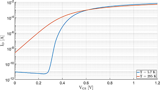
Figure 13. Drain current ( ) in saturation regime versus gate-to-source voltage (
 ) in a n-channel field-effect transistor (FET) fabricated in state-of-the-art 65 nm CMOS technology. The device was tested both at room temperature (295 (K) and at the minimum cryogenic temperature achievable with the available equipment (5.7 (K) as a part of our characterization and modeling campaign. The FET channel is 10 µm wide and 100 nm long. Despite the absence of cryogenic anomalies, the effect of temperature still creates a very clear difference, especially for low gate voltages.
Download figure:
Standard image High-resolution image5.3. Cryogenic test bench
Since the main prototype of the E-TEST will take several days to reach the targeted vacuum and temperature, a cryogenic test bench is used to test the cryogenic components. This will allow the components to be quickly tested, adjusted or repaired outside the chamber. The minimum temperature achieved was  . The setup was capable of maintaining a minimum pressure level of
  during cooling. A typical cooling of the cryostat takes about
  . After cooling, the temperature is stable within
  . The fluctuations are caused by the cyclic nature of the cooling process. The setup is capable of achieving a temperature of
  with an additional heat load of
  which is well above the required design value of
  design value. More information on the design, cooling process, and operation, see this article [68].
6. Low-noise optical technologies
In addition to the mechanical technology described in the earlier chapters, also the necessary optical technology for low frequency ET will be developed and demonstrated within the E-TEST project. The suspended mirror in cryogenic environment is made of silicon, which is opaque to the conventionally used wavelength of 1064 nm. A new laser wavelength in the range of approximately 1500–2000 nm is needed, which will not be absorbed within the silicon mirror. Resulting from this, new photodiodes and coatings have to be developed.
Since the mirror shape might change when cooled down to the required cryogenic temperature, also a new interferometric sensor measuring this behavior is in development. Within E-TEST, a laser at a wavelength of 2090 nm, consisting of a crystal based Ho:YAG seeder and a highly-stable holmium-doped fiber amplifier will be developed [25]. Therefore, the sensors and the coatings are also optimized to fit to the laser wavelength to enable a high level of synergy.
In the following chapters, these innovative technologies will be described in details and the three big key experiments for the technology validation will be presented.
6.1. Lasers at 2 µm
To achieve the desired parameters, we plan to set up a MOPA (Master Oscillator, Power Amplifier) system, containing a crystal-based seed laser and fiber-based amplifiers. For wavelengths  m, for example Tm-doped crystals can be used for the generation of the radiation. However, the drawbacks of these crystals are the inherent amplitude instabilities, which limit the output power stability [69, 70]. As an alternative to fulfill the desired power stability requirements, we plan to use Ho-doped crystals, which can be less sensitive to mechanical and atmospheric disturbances due to their higher gain cross section [71]. By using a Ho-doped crystal, for example a wavelength of 2090 nm can be realized.
For further power scaling, we aim to use holmium-doped fiber amplifiers, which can for example be pumped by thulium-doped fiber amplifiers at a wavelength of app. 1950 nm. This way, the quantum defect can be as low as app.  , which can result in an overall higher output power stability due to a lower impact of thermal effects within the fiber amplifier.
In the E-TEST project, a multi-stage MOPA will be developed to fulfill the laser requirements.
In most GW detectors, lasers at a wavelengths of 1064 nm are commonly used as beam sources. However, at a wavelength of 2090 nm, the development of lasers is not that advanced, which for example results in fiber components with typically worse performance parameters in comparison to 1064 nm fiber components. Within the E-TEST project, we aim to develop an innovative laser system with the following parameters:
- Wavelength: 2090 nm
- Power: 5–10 W
- Spectral linewidth: 1 kHz
- Relative intensity noise (RIN):
 10−6 HzHz 100 Hz
 - Frequency noise: 100 HzHz 100 Hz (assuming 1/f spectrum)
- Degree of linear polarization: 98%.


6.1.1. Laser design.
To achieve a wavelength of 2090 nm, holmium can be used as an active dopant in crystals and fibers. For the pumping of the holmium-doped crystals and fibers, thulium-doped lasers at a wavelength of 1950 nm. This can result in a very low quantum defect, providing a potentially low thermal-noise laser.
Therefore, we develop a solid-state laser based on Ho:YAG crystals as a seed laser, which defines the spectral properties. For the power amplification, a two-stage fiber amplifier based on holmium-doped fiber is developed. Figure 14 shows the scheme of the full laser concept. In addition to the mentioned seed laser (Seeder) and the two amplifier stages (Ho1 and Ho2), pump lasers for Ho1 and Ho2 have to be used and developed (Tm1 and Tm2). These pump lasers are thulium-doped fiber lasers at a wavelength of approximately 1950 nm. For the pumping of the crystalline Ho:YAG seeder, an earlier developed Tm:YLF laser will be used. The benefit of the multi-stage MOPA setup is its high adaptability. Depending on the output power of the seeder, one or two amplifier stages can be used. Within the development, different concepts are tested and compared to find the most practical and satisfying solution.
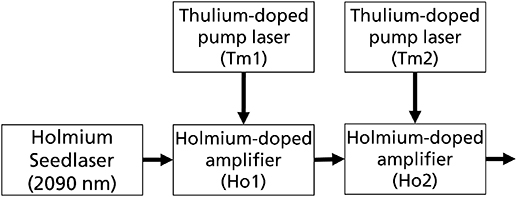
Figure 14. Model of the laser concept. Within the Ho:YAG seeder, the spectral properties are defined. This will result in a low bandwidth and a wavelength of 2090 nm. Within the Ho-doped amplifier Ho1 and Ho2 the power will be amplified.
Download figure:
Standard image High-resolution imageTo fulfill the high requirements on linewidth and stability, we aim to develop a non-planar ring oscillator (NPRO) seed laser. To achieve this, the development is divided in two phases. While state of the art NPROs at 1064 nm show satisfying results with respect to stability and linewidth, development at 2090 nm based on Ho:YAG crystals is still an ambitious approach. Therefore, in the first phase, a ring oscillator will be developed. Such a concept has a significantly higher success probability and the power amplification within a fiber resonator can be gathered. In the second phase, a compact and thermally stable NPRO will be setup and investigated to achieve the higher stability and lower linewidth.
Thanks to their compact design and achievable output powers, monolithic fiber amplifiers are a good technology to achieve a high stability at high power levels. The multi-stage fiber amplifier itself is designed to amplify low power signals of 1 mW, e.g. delivered by the NPRO, to more than 500 mW in the first stage, and to more than 10 W output power in the second stage. The fiber diameters are adapted to enable high amplification and mitigate stimulated Brillouin scattering. Since the required RIN is very ambitious, the output power of the NPRO seeder and all fiber amplifier stages will be actively controlled.
6.2. Low-noise coatings
In order to provide the best performance, the optical coating must assure the lowest possible contribution to noise due to absorption. Many crystalline materials show lower optical absorption and mechanical loss than amorphous materials. However, the low and high reflective-index materials have to be lattice matched, and this limits the number of available options. Crystalline coatings made of AlGaAs and GaAs are under investigation and show promising performance [72]. The requirement of a lattice matched substrate—GaAs wafers in case of AlGaAs coatings—for the growth procedure requires a transfer of the coating to a suitable substrate after production and also can limit the maximum coating size (to about 20 cm in case of GaAs). Defects in the bond for attaching the coating to the new substrate can lead to the coating detaching during the test-mass cooling procedure or to thermal noise from a change in bulk and shear loss.
Part of the approved E-Test budget proposal is dedicated to the construction of a novel molecular beam epitaxy (MBE) coating facility to investigate new crystalline coatings for application in future GW detectors [73]. Crystalline oxide coatings will be developed with the MBE coating facility. The layers are likely to be more sensitive to the differential thermal lattice expansion between the mirror body and the coating in comparison to amorphous coatings. Therefore it will be important to test whether the crystalline coatings survive well to repeated heating and cooling cycles without the appearance of cracks. Furthermore, in all likelihood, the crystalline oxide coating will need to be bonded to the mirror body and this bond might be a fragile place where the wafer could detach with repeated temperature cycling. Another topic of investigation is whether the optical properties drift as a function of time with continued long-term exposure to ultrahigh vacuum and low temperatures and whether a protection layer will be needed.
6.2.1. MBE coating.
The general working principle of the MBE process consists in bombarding a rotating and heated substrate with a beam of atomic of molecular (precursors) species emanating from an effusion cell [74]. An effusion cell is essentially a crucible in which the material to be evaporated is inserted combined with a heating element wrapped around it and a shutter that opens and closes the path to the substrate. The deposited species on the substrate then react with oxygen species (atomic oxygen, molecular oxygen or ozone) emanation from a gas inlet, to form on oxide film. The structure of the growing film is then monitored in real-time using an electron diffraction pattern created on a screen with a technique called reflection high energy electron diffraction [74, 75].
The main advantages of oxide MBE include a low background (10−11 Torr) and operational pressure (10−8–10−5 Torr). This enables an excellent control on (gaseous) contamination as well as oxygen content in the layers. For instance it allows to grow suboxides, i.e. oxides that do not have the highest oxidation degree; but many of which have a higher refractive index. In addition, it permits a good control on the oxidation modulation in a coating. Moreover, it offers a low energy deposition process, an excellent uniformity control at or below 1 , directed beam deposition and in-situ thin film characterization tools.
6.3. Photodiodes
An important active part of the interferometer is the light detector. The photo detector detects photons exiting the interferometer at the dark fringe and thus it is susceptible to the photon number variations caused by the interaction of the GW with the interferometer. The infrared wavelength of 2 µm is one of the main innovation of the E-TEST development as it couples to requirements imposed by the low temperature operated Si mirrors and auxiliary optics. This allows for a significant reduction of the vibration noises at temperatures 5–20 K. To match the laser wavelength, a detector with an optimal spectral dependence and quantum efficiency needs to be chosen.
6.3.1. Proposed procedure.
The low temperature operation allows for a significant reduction of the technical noise and thus improving the signal to noise (S/N) ratio as well as allowing to widen the operational frequency for the GW detection. For optimizing the detection wavelength, we built two different detection setups, a classical lock-in detection and a homodyne detection. These systems are operational and being used for extensive detector testing. The testing involves the characterization of the dark current of the device that contributes to the noise level. Extensive testing were executed with the InGaAs detector, to optimize the detector circuitry: the developed pre-amplifier has a bandwidth of 10 kHz and a noise level of a 500 aW/ . This will give a theoretical
  1011 noise suppression in the expected currents measured by the photodiode.
7. Validation of optical instrument
The suspended silicon test mass will be subjected to three optical experiments shown in figure 15 to validate several aspects of the system. The three experiments are (a) mirror surface characterization using white light interferometry, (b) measurement of the mirror thermo-optic properties and (c) mechanical quality factor measurement on the silicon mirror.

Figure 15. The three optical experiments: (a) the white light interferometer, (b) the temperature measurement and (c) the quality factor measurement. Contrary to the suggestions of this figure, all experiments probe the same side of the mirror, having access through the 3 tubes into the cryostat visible in figure 2. Prior to hanging in the cold suspension, experiment (a) will also probe the full mirror surface, but on an optical bench outside the cryostat.
Download figure:
Standard image High-resolution image7.1. White light interferometry to characterize the mirror on operation
The induced vibrations and wavefront or topology change are two issues that may appear consequence of cooling down the suspended mirror. In the framework of the ET, a mirror characterization is essential to ensure the accuracy of the results in the detection of GWs. We develop a metrology instrument for the E-TEST project to characterize the cryogenic mirrors for a GW detector in operation. The metrology instrument measures the local vibration as well as the topology change of the suspended silicon mirror at cryogenic temperatures. The instrument is a low-coherence interferometer that does not use movable components to avoid additional unwanted vibrations. It includes an innovative optical phase mask to capture on a single camera frame a set of interferogram maps of the same area observed on the test mass at different optical path differences. The optical phase mask works in transmission. It has a stair shape made of steps of different optical thicknesses of the same material. Each step on the optical phase mask simulates a different position of a conventional piezoelectric (PZT) device for surface scanning [76]. The envisaged first optical phase mask has 49 steps in a 7-step by 7-step square shape, equivalent to 49 interferogram maps of the area observed on the test mass. The spot size of the beam incident on the test mass has a diameter of 1 cm. A schematic representation of the metrology instrument, based on the optical layout of a Michelson Interferometer, and the phase mask, is included at the left of figure 15. Another critical component of the instrument is a microlens array of 49 lenses in front of the detector to image the information of each step.
We use a low-coherence source to determine the mirror location unambiguously and, therefore, the local vibration and topology. The interference pattern of a low-coherent white light source has a well-differentiated central fringe visible only when the optical paths of the two arms of the interferometer are almost exact. This region of fringe visibility, in our case around 1 µm width, is determined by the coherence length of the source. The difficulty in obtaining the interference fringes with a low-coherence source is an advantage to avoiding spurious unwanted interferometry signals from scattered rays, speckle, dust, and imperfections [77].
Each step of the optical phase mask we design will capture a point of the interference pattern. Then we reconstruct the full interference pattern. We do this at multiple local points inside the area observed at the test mass. The interferogram map of each step is 30 px by 30 px. Therefore, we have the information on local vibration and topography of 900 different local points inside the area observed of the test mass, which is around 1 cm in diameter. Due to the complexity of the optical phase mask, we expect defects and dissimilarities between steps besides test mass deformations. Due to these two factors, we measure unequally spaced sample points on the white light interferograms. To solve this, we develop new processing algorithms for the interference patterns to reach a vertical resolution of a few nanometers. [78] includes a detailed explanation of measuring vibration and topology change, besides an introduction to the analysis algorithms we develop.
We use the metrology instrument to measure low-frequency vibrations around 10 Hz. We develop subtraction methods and use signal modulation to minimize the effect of the noise from the optical table and other components on the measurements. For the deformation measurements, the lateral resolution will be a few micrometers, according to the pixel size of the detector. A prototype of the metrology instrument with an optical phase mask of 25 steps is currently under development.
7.2. Measurement of the thermo-optic properties of the silicon test mass
Due to its high refractive index of around 3.5 at a wavelength of 2090 nm, the boundary between silicon and air reflects around 30 of light. The two surfaces of the silicon test mass form a Fabry–Pérot etalon, where light bounces back and forth. The individual light fields interfere constructively or destructively, depending on the optical path for one round-trip. As the silicon mirror is cooled down, this optical path changes due to two effects: an expansion of the material due to temperature, described by the thermo-elastic coefficient α = dL/dT, and a change in refractive index, described by the thermo-refractive coefficient β = dn/dT. Together, they form the thermo-optic coefficient of the silicon material. This thermo-optic coefficient can be measured by monitoring the interference fringes of the etalon, together with the substrate temperature [79]. Tracking the fringe pattern to measure the thermo-optic coefficients, was performed in [79]. We plan to do it in a similar way: we will start with the reconstruction and fitting of the full fringe data at room temperature and analyze the measured fringes as they pass through using the temperature-dependent coefficients. These can be compared to and correlated with conventional temperature sensor data, to further calibrate and validate the measurement, as the temperatures measured conventionally at the edges of the substrate and the middle of the substrate will not be vastly different, and especially will converge after long cooling times. Knowing the thermo-optic coefficient, the observed interference fringes can be used to obtain the temperature evolution of the silicon substrate, which allows for a contactless measurement and monitoring of the silicon temperature at the location of the laser beam. This is especially relevant for E-TEST, where we are interested in the temperature gradient during cool-down, but at the same time we cannot place conventional temperature sensors all over the test mass without impacting the performance of the seismic isolation, and more importantly, destroying the optical and mechanical quality of the mirror itself. This is why we adopted a non-contact methodology, using a µm laser source orthogonally shining the mirror surface: the beam will interfere with itself when it is reflected back and recorder via a photodetector.
7.3. A mechanical quality factor measurement of the silicon substrate
Another way of probing the quality of the mirror substrate is by exciting its mechanical internal modes and see how much energy they dissipate per cycle of the kHz mode. A tiny hammer, i.e. a small mass with a spring element that can be made with e.g. a coil magnet actuator to tap the test mass ever so slightly, can excite all modes that do not have a node at the position of hammer impact. Once the modes are excited and ringing down it is up to an optical measurement to determine the envelop of the exponentially decaying ring-down.
The optical setup to do perform such measurement is depicted in figure 15(c). An interferometer uses polarizing optics to divert the light of both arms to two photodiodes [80]. The error signal is generated by subtracting the two out-of-phase photodiode output signals. This ensures all common mode noises—typically laser noises such as amplitude fluctuation—are decreased to shot noise level. The error signal is used to make the mirror attached to a piezo actuator follow to probed mirror point, such that the signal sent to the piezo actuator will show a ring down indicative of the mirror mechanical loss. Such interferometric readout systems can reach 4 fm/ Hz sensitivity [51] which is sufficient as the hammer can induce large enough internal-mode-associated mirror surface motion.
A fiducial loop design is shown in figure 16(a) with a bandwidth of 13 kHz allowing for a proper measurement of the first ten internal modes of the 100 kg, 45 cm diameter silicon mirror. The signal sent to the piezo actuator holds a superposition of all the different modes, which can be isolated using a bandpass filter. By finite element analysis, such as shown in figure 16(b), the frequency of each mode can be compared and the mode shape identified. This will also show which part of the mirror substrate (face) will move with a large enough amplitude for our sensitivity and an estimation of the expected signal strength can be made. The laser probe position on the mirror front surface can be varied by using the three different access tubes through the cryostat.
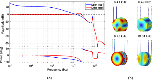
Figure 16. (a) Bode plot of a feedback loop comprised of a piezo actuated mirror ( f
 = 80 kHz) a high voltage amplifier (gain of 100) and a standard PI servo, a low pass filter at 1 kHz, an elliptical filter (Q = 0.88 pole at 25 kHz and Q = 50 zero at 136.25 kHz) and Butterworth filter at high frequency. (b) Finite element analysis of the mirror internal modes; the 1 s mode at 6.41 kHz, the 2nd at 6.49 kHz, the 8th mode at 9.75 kHz and the 10th mode at 10.61 kHz are shown.
Download figure:
Standard image High-resolution image
8. Conclusion
The research described in this paper presents the activities of E-TEST project on a single cryogenic suspension of an ET-sized silicon mirror. These activities include the development of a compact isolator, the radiative cooling of a large cryogenic mirror (100 kg), and the technical development of the operation of the laser at 2090 nm. These key technologies being developed and tested will influence the design aspects of next-generation GW detectors, particularly at low frequencies.
The novelty of the seismic isolation system, which makes use of a combination of an actively isolated platform and an IP, would allow to suppress the seismic motion thanks to the pair with ultra-performative sensors and actuators (1 pm resolution at 1 Hz).
The cryogenic environment provides an ideal operating conditions for the suspended mirror, thanks especially to the reduced thermal noise: to assure that the cooling process will not induce vibrations on the test mass, an innovative technique based on radiative cooling was designed.
The optical and readout designs were adapted according to the requirements imposed by the silicon material: an advanced technology is under development to satisfy the high level of quality for the optical components and photodiodes to work with the new 2 µm wavelength.
The facility is being built at the Centre Spatial de Liége in Belgium and it is aimed to provide crucial tests for the new science exposed.
Acknowledgment
This work comes within the scope of the E-TEST project, which is carried out within the framework of the Interreg V-A Euregio Meuse-Rhine Programme, with  million from the European Regional Development Fund (ERDF). By investing EU funds in Interreg projects, the European Union is investing directly in economic development, innovation, territorial development, social inclusion, and education in the Euregio Meuse-Rhine region. For a thorough review, the authors would like to thank European Union for this support and investment. This paper can be referenced to this LIGO DCC Number LIGO-P2200399.
Data availability statement
The data that support the findings of this study are openly available at the following URL/DOI: https://arxiv.org/abs/2212.10083.