
Abstract
We present a process to manufacture solenoidal microcoils with external support structures, which leaves the space within the coil windings free. The manufacturing procedure is based on a two solvent approach (water and acetone), for selectively etching polyvinyl alcohol and polymethyl methacrylate. Two sets of microcoils were manufactured with an inner diameter of 1.5 mm, an interwinding pitch of 100 μm and five or eight coil windings respectively. The coils were designed for application in magnetic resonance imaging and spectroscopy, and characterised in a 9.4 T MR scanner. An NMR spectrum of water and MR images in receive only and transceive mode were acquired as proof of concept.
Export citation and abstract BibTeX RIS

Original content from this work may be used under the terms of the Creative Commons Attribution 3.0 licence. Any further distribution of this work must maintain attribution to the author(s) and the title of the work, journal citation and DOI.
1. Introduction
With the introduction of microcoil detectors in magnetic resonance spectroscopy (MRS) and imaging (MRI), the sensitivity of detection was increased for mass and volume limited samples [1–4]. In MRS and MRI, solenoidal coils—conductors wrapped around a support structure—are preferred for their excellent B1-field uniformity, B1/i field efficiency, and the resulting high signal-to-noise ratio (SNR). Though Olson et al showed that the use of microcoils can increase the mass sensitivity of MRS measurements considerably [5], solenoidal microcoils have not yet made their way to commercial success. One reason for the lack of such products is the tedious manufacturing procedure, in which the coils are wound by hand, thus decreasing manufacturing yield and reproducibility. Manual winding also makes the manufacturing of microcoils with defined and precise interwinding distances difficult, which is a limiting factor for some advanced MRS methods (e.g. dynamic nuclear polarisation (DNP)). The use of automatic wirebonding offers one solution to these problems [6]. Wirebonders have exceptional precision and their speed provides high throughput and repeatability in microcoil manufacturing.
Another drawback of 3D manufactured solenoidal microcoils is the necessity for an internal winding support structure, such as a pillar (the coil yoke) around which the coil wire can be wound, which inherently decreases the available sample volume that generates the NMR signal [6]. A smaller sample volume in turn decreases the signal-to-noise ratio (SNR) of the microcoil, which is proportional to the filling factor  . As coil dimensions are downscaled, the relative size of the yoke necessarily increases, because the required minimal mechanical strength limits the cross-sectional area of the pillar [6, 7], thus occupying even more of the inner volume. To overcome the issue of decreasing filling factors, in particular for microcoils, it would be advantageous to support the microcoil from the outside, leaving the inner volume free for the sample (figure 1). This paper establishes a new manufacturing process, by using a sacrificial layer and a combination of two solvents, water and acetone, yielding hollow microcoils encased in external support structures.

Figure 1. Solenoidal microcoils with internal and external support structures.
Download figure:
Standard image High-resolution imageManufacturing techniques based on sacrificial layers such as silicon dioxide or porous silicon have found wide use in the manufacturing of MEMS devices, which usually require expensive machines or special and often toxic solvents, e.g. hydrofluoric acid (HF), sodium hydroxide (NaOH) or potassium hydroxide (KOH) [8–11]. As a result, the use of polymers as sacrificial layers for the manufacturing of a variety MEMS devices has increased in recent years. Typically, polymers do not need special solvents for etching, but rely on chemicals (such as acetone and water) that are widely available in most laboratories.
Bagolini et al [12] used polyimide (PI) as sacrificial layer. It was applied as thin film, with a thickness of up to 4 μm. PI is very stable against a variety of etchants, such as acetone and HF. The release of the sacrificial structure was done with an O2-plasma etch, which is selective for patterning metals, but not for patterning different kinds of polymers.
A straightforward method for manufacturing thick photopolymeric SU-8 structures was presented by Patel et al [13]. They used silicone as the sacrificial layer, which was removed simply by peeling off the silicone after curing the SU-8. This process relied on the low adhesion between SU-8 and silicone.
Linder et al published a process using neutralised polyacrlyic acid (PAA) as a water-soluble sacrificial layer [14]. PAA has very high solubility in water, and thus a high etching rate. However, in our experience, PAA does not work well if used for thicker structures, due to its high volume shrinkage. Additionally, for thick structures, it is prone to trap air bubbles, since during drying the fluid rapidly develops a solid film at the PAA-air interface, thus trapping the bubbles.
Ferrell et al [15] used a thin layer (750 nm) of polyvinyl alcohol (PVA) as a water-soluble sacrificial layer. PVA is a suitable material for manufacturing larger structures, since it can be cast, extruded and deformed under an elevated temperature. The volume shrinkage is significantly lower than PAA. For example, based on a rough calculation using the density of the polymer and the mixing ratio with water, the volume shrinkage of PAA is 73%, while it is 54% for PVA. PAA becomes brittle once it is dry, so that care must be taken with the application of forces during subsequent processing.
All of the cited publications used sacrificial layer thin films, with thicknesses in the lower μm range. Microcoil posts are typically >100 μm, and as such the published processes are not transferable to the creation of these thicker, more voluminous structures.
2. Manufacturing procedure
2.1. Overview
Our process builds upon previously published wirebonding technology to automatically form microcoils [16–20]. Water-soluble PVA support structures replace SU-8 as the coil yokes. After wirebonding, the structures are embedded in polymethyl methacrylate (PMMA), which forms the external support structure. The sacrificial PVA structures are then removed, leaving the metal windings as the inner wall of the coil (see figure 2). The manufacturing steps are summarised in table 1.
Table 1. Overview of the casting procedure.
| No. | Step (+Description) | Parameters |
|---|---|---|
| 1 | Cast PVA posts | |
 |
FR4-board anchors posts drilled PMMA mould attached with Al press syringe dispensed PVA | Mix PVA/water 50/50 wt% heat mixture to 75 °C fill syringe and dispense dry 24 h at 2.5 bar at 55 °C |
| 2 | Dissolve PMMA mould | |
 |
Put set-up in acetone bath bottom up | Acetone bath for 24 h Rinse with clean acetone |
| 3 | Glue substrate chips | |
 |
Glue substrate chips to PCB With neutralised water- soluble PAA (see [14]) | 6 μl of neutralised PAA
Dry 12 h at  |
| 4 | Wirebond microcoil | |
 |
Special frame for substrate fixation | At 125 °C |
| 5 | Cast PMMA support | |
 |
PDMS form as casting mold seal PDMS mold off by press PMMA = Paladur® | Mix powder & Fluid for 10 s dispense mixture with syringe cure 12 h at 2.5 bar at 55 °C |
| 6 | Polish PMMA support | |
 |
Use polishing frame | Grain size P180 to P1200 polish 9 μm to 3 μm |
| 7 | Dissolve PVA posts | |
 |
Place set-up in clean water | Dissolve 24 h at 55 °C |
2.2. Substrate preparation
Although many different substrates are compatible with the two-solvent process, the choice was limited by constraints imposed by MRS and MRI. Mismatches in the magnetic susceptibility of substrate and water lead to line broadening and imaging artifacts. We selected a 100 mm diameter Pyrex wafer substrate, with a thickness of 500 μm. Alternatively, the use of other materials, such as silicon or printed circuit boards, would be feasible, but due to their susceptibility mismatch with water, they are less suitable for the MRS environment.

Figure 2. Rendered CAD model of the externally supported microcoil mounted on the Pyrex substrate.
Download figure:
Standard image High-resolution imageFirst, a 50 nm chromium (Cr) film, acting as an adhesion layer between Pyrex and gold (Au), and subsequently, a 150 nm Au seed layer were deposited onto the wafer by chemical vapour deposition (CVD). Following this a 20 μm AZ 40XT positive photoresist (MicroChemicals, Germany) was spin-coated onto the wafer and patterned5.
A 15 μm Au layer was electrochemically deposited into the AZ 40XT mold. After electroplating, the photoresist was stripped for 15 min with the dedicated resist remover TechniStrip NI555 (MicroChemicals, Germany), and subsequently rinsed with acetone, iso-propanol and DI-water.
To provide discrete electrical contacts and bond-pads, the Cr/Au seed layers were removed by wet-etching first in a potassium iodide solution, and then in a standard chromium etchant solution (TechniStrip Cr01, Microchemicals GmbH, Germany). The wafer was then diced into single chips with a wafer saw equipped with a 200 μm dicing blade. Since the substrate chips needed a hole and a rounded top for the subsequent steps, these structures were powder blasted. A custom milled aluminium sheet was used as the masking layer for powder blasting.
2.3. Two-solvent process
We evaluated the cross selectivity of the etchants by placing a block of cured PVA and an FR4 board in acetone, and a block of PMMA in water, both for 72 h. We found no visible changes in either of the materials, thus concluding the solvents feasible for the process.
In preparation for the PVA cast (step 1), an FR4 board was prepared by milling round cavities into the board, which later acted as anchors for the PVA cast (see figure 3). The board was made of FR4 (Bungard Elektronik GmbH, Germany), a glass-reinforced epoxy laminated sheet, usually used as base material for printed circuit boards (PCBs).

Figure 3. Cast PVA posts on a FR4-board. The substrates are aligned with an aligmnent frame.
Download figure:
Standard image High-resolution imageSince we cast PVA directly by dispensing it from a syringe, we manufactured the PMMA mold by precision milling. This mold was attached to the FR4-board with a simple press made from aluminium, which ensured vlose contact between the FR4-board and PMMA mold. Alignment of the two was achieved with precision pins.
The PVA for molding was prepared from 50 wt% PVA filament (Makerbot Industries LLC., USA) mixed with 50 wt% deionised water, sealed air tight, heated to 75 °C, and stirred for 12 h. Then, the solution was dispensed into the prepared PMMA mold with a syringe. To avoid bubble formation while drying, the whole set-up was placed into a pressure chamber, at 2.5 bar for 24 h at 55 °C.
After drying, the set-up was removed from the aluminium press, and placed into an acetone bath for 24 h to dissolve the PMMA (step 2). Since the solved PMMA settled on the bottom of the acetone bath, the set-up was placed upside-down in a slightly elevated position. After 24 h of etching, the FR4-board was rinsed with fresh acetone to remove any PMMA residue.
Since the coil requires the substrate to have a through hole, and the microcoils are wound with an automated wire bonder, the substrate chips were glued (step 3) to the FR4-board with PAA. An alignment frame was placed on the FR4-board for positioning the substrates (figure 3). Then, 6 μl PAA was dispensed with a pipette on the FR4 board, and the substrate was pressed on the FR4 board, thus spreading the PAA. The set-up was then dried in an oven for 12 h at 55 °C.
The FR4 board with the attached substrates was mounted onto the hotplate of an automated wire bonder (ESEC Wire Bonder 3100 plus). For the wire bonding process (step 4), an array of the prepared substrates (figure 4) were clamped and heated to 125 °C, which is required for the wire bonding process to work. A 25 μm diameter insulated gold wire was wound around the PVA cast posts to achieve solenoidal microcoils with five or eight windings each. To increase the wedge adhesion, an additional ball bond was bonded on top of the wedge bond.

Figure 4. Bottom: array of wire bonded microcoils, wound around PVA posts. Upper right: magnified view of one of the wire bonded microcoils. Upper left: secured wedge bond.
Download figure:
Standard image High-resolution imageAfter wire bonding, a mold made from polydimethylsiloxane (PDMS) Elastosil m4642 (Wacker Chemie, Germany) was placed on top of the array of wire bonded microcoils. For PMMA casting (step 5), we used the fast curing and easy to handle PMMA Paladur® (Heraeus Kulzer, Germany), usually used for dental prostheses. Paladur® has two major advantages over other PMMA casting compounds: it exhibits a very low volume shrinkage, and bubble formation is easily preventable by the use of a pressure chamber.
The PMMA raw materials were mixed according to the recipe given in the data sheet. 1 g of powder (methylmethacrylate co-polymer) and 0.6 ml of fluid (methylmethacrylate, dimethacrylate) was stirred for 10 s. A syringe was then filled with the mixture, and this was immediately dispensed into the mold. Then the set-up was placed into a pressure chamber at 2.5 bar, and cured for 12 h at 55 °C.
To remove overflowing PMMA residue from the casting, the whole set-up was mounted onto a polishing frame (step 6). The substrates with the PMMA cast were then ground with sand paper, with grain sizes of P180 to P1200, and subsequently polished with suspension and a particle grain size down to 3 μm.
Finally, the array of PMMA embedded wire bonded microcoils was submerged in DI-water (step 7) to dissolve the PVA structure. The water container was heated to 55 °C and after 24 h the PVA and the PAA were completely dissolved. The single substrates were rinsed in DI-water for final cleaning. Figure 5 shows the resulting externally supported wire bonded microcoils.
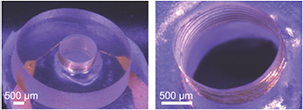
Figure 5. Left: wire bonded microcoil with external support to maximise the filling factor. Right: close-up view of the microcoil windings (with an inter winding pitch of 100 μm).
Download figure:
Standard image High-resolution image2.4. Failure mechanisms
Figure 6 depicts the most prominent failure mechanisms the authors experienced during the development of the process. For the process to succeed, it was essential to use PMMA casting materials that do not require two liquid components to be cross-linked. Cross-linking chemistry can lead to a high volume shrinkage, as is depicted in figure 6(b). For these experiments, liquid two component cross-linking PMMA resin was used (S u. K Hock GmbH, Germany). Due to the high content of solvents, volume shrinkage is high, thus requiring multiple casts. Since the solvent does not cross-link, but evaporate, a film of hardened acrylic material developed on top of the cast. This prevented arising gas bubbles, presumably from solvents in the volume bulk, to escape from the cast. Additionally, when using the PMMA resin by S u. K Hock GmbH, Germany, the PVA is absorbed by the PMMA (see figure 6(a)).

Figure 6. (a) Absorbed PVA during PMMA cast. (b) Very high volume shrinkage of PMMA. (c) Residue of air bubbles in the PVA cast. (d) Nose-like PMMA structure that leaked into the PVA.
Download figure:
Standard image High-resolution imageBoth of these problems can be prevented by using casting materials used in dental healthcare for temporary prosthesis, which are based on a liquid and a powder component (we used Paladur® by Heraeus Kulzer, Germany). However, if the PVA cast is not completed carefully (e.g. by casting at atmospheric pressure), it will also generate air bubbles in the cast, which will be filled in the subsequent PMMA casting step (see figures 6(c) and (d)).
3. Results
Two sets of hollow microcoils were manufactured with the described procedure. Both sets of coils had an inner diameter of 1.5 mm and an inter winding pitch of 100 μm. While the coils of the first batch had eight windings, the second batch of coils only had five windings.
The self-resonant frequency (SRF) was measured inductively, using a 1 cm diameter pick-up coil connected to a USB vector network analyser (miniVNA Tiny, miniRadioSolutions.com). The self-resonant frequencies were extracted from S11 reflection measurements and five coils of each batch were analysed. For the first batch with eight windings we measured  , and
, and  for the second batch with five windings. Q-factors were determined using the procedure described by Haase et al [21]. At the resonators' self-resonant frequency, we measured
  and
and  . As the coils were designed for magnetic resonance imaging and spectroscopy measurements, they were then consecutively tuned to 400 MHz, which is the 1H proton resonance frequency at 9.4 T (Larmor frequency), and matched to 50
  (figure 7). The Q-factor after tuning and matching was
  .
.

Figure 7. S11 curve of a hollow micro-coil, tuned and matched to 400 MHz and 50 Ohm.
Download figure:
Standard image High-resolution imageMagnetic resonance experiments were carried out using a conventional horizontal bore 9.4 T Bruker BioSpec 94/20 USR (Bruker BioSpin, Ettlingen, Germany), commonly used for preclinical animal imaging. As a figure of merit in magnetic resonance spectroscopy, the full-width-half-maximum (FWHM) line-width of an MR spectrum of pure water was recorded, as shown in figure 8. The FWHM line-width of 0.081 ppm, which corresponds to 32.43 Hz at 400 MHz, is a measure for the spectral resolution. A nutation spectrum, sweeping the excitation pulse length, while keeping the excitation pulse power constant at 0.625 mW, was used to determine an excitation pulse length of 140 μs for the 90° flip angle. The envelope function of this spectrum has the wavelength of the nutation frequency. The period of the envelope function is measured to be  s, and thus the nutation frequency is
  Hz. Using the gyromagnetic ratio of protons of
  MHz T−1 and the equation
  taken from [22], the r.f. field strength can be calculated to be
  μT, where
  is the angle of the B1 field w.r.t the static magnetic field. The B1 field strength can be normalised with the square root of the applied excitation pulse power, thus giving the r.f. efficiency of the microcoil
  μT
μT  , where
  .
.
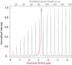
Figure 8. NMR spectrum (red, lower scale) and nutation spectrum (grey, upper scale) of water, recorded in a horizontal bore 400 MHz Bruker biospin system with the manufactured micro-coil.
Download figure:
Standard image High-resolution imageAs proof of principle, two sets of magnetic resonance images were taken. First the microcoils were used in a receive only set-up, meaning the transmission of the r.f. pulse was delivered by a large volume coil with an inner diameter of 89 mm. Using a common FLASH sequence [23], 64 averages and a scan time of 10 min 40 s we obtained a spatial resolution of  . The two receive only MRI sections, coronal and axial, through a coil are depicted in figures 9(a) and (b), where the coil windings are clearly visible as high intensity signal peaks.

Figure 9. Coronal and axial MRI sections through a hollow micro-coil in receive only ((a) and (b)) and in transceive mode ((c) and (d)).
Download figure:
Standard image High-resolution image
The second set of magnetic resonance images were taken in transceive mode, i.e. without using the larger r.f. coil for excitation. Again a FLASH sequence was used, and 64 averages were taken resulting in an overall scan time of 26 min 38 s and at a spatial resolution of  per image (depicted in figures 9(c) and (d)).
4. Discussion
We processed with PVA as a key intermediate stucture. It has a melting point at 200 °C and a glass transition temperature at around 85 °C. This limited the maximum temperature of the wire bonding step. We processed at 125 °C to bond 25 μm diameter gold wire, where the PVA became soft, but was still controllable. When transferring this process to higher temperatures (for example for copper wire bonding) or thicker wire diameters, PVA will need to be replaced by another water-soluble polymer with better temperature stability.
The Q-factor after tuning and matching was 44. Embedding a microcoil in PMMA can diminish its Q-factor, since replacing the air between windings with PMMA (higher dielectric loss tangent) increases capacitance and parasitic losses. This effect becomes prominent at frequencies approaching self-resonance, where a significant fraction of the energy is stored in the electric field [24]. It is well known that, for increasing frequency, a microcoil resonator passes from inductive to capacitive behaviour at its self-resonance frequency. The microcoil behaves primarily as an inductor at its working frequency of 400 MHz, which is well below its self-resonance of 1 GHz, and hence its performance as MRI detector should remain relatively unaffected. The manufactured microcoils were characterised by recording an NMR spectrum and MR images of water. The resolution is measured to be 0.081 ppm, which is competitive with other devices at the micro scale, but it is not yet sufficient to acquire high resolution spectra [25]. The r.f. efficiency of 3355 μT  is competitive with published reports on similar devices, such as the probehead by Ryan et al [26], with an efficiency of 184 μT
  , Sakellariou et al with an efficiency of 2030 μT
  [27] and Sillerud et al with an efficiency of 1897 μT
  [28].
[28].
The imaging experiments demonstrate the straightforward compatibility of the microcoils with the MR scanner, and their ability to acquire high-resolution images. However, the high intensity peaks in figures 9(a) and (b) show the influence of coil wire, which is in close proximity to the sample volume, so that for very small microcoils these artifacts will have to be compensated. One way to diminish the artifacts is to use copper wire, rather than gold, since the magnetic susceptibility of copper is closer to that of water. Passive shimming might be used to compensate these artifacts further [29].
With the process presented, microcoils with a filling factor of 100% are possible, which is an essential step towards achieving further miniaturisation. Kratt et al published two papers on microcoils manufactured by wire bonding, one with PMMA posts as coil yokes manufactured by deep x-ray lithography, a very expensive and time-consuming method [30]. The minimum wall thickness for these yokes was found to be 20 μm, thus permitting a filling factor of 94.7% for a 1.5 mm microcoil. However, using SU-8 as coil yoke, with wall thicknesses down to 60 μm, reduces the filling factor to 84.6% [6]. Sillerud et al used lithographically patterned microcoils on glass capillaries as NMR detectors. With a glass capillary diameter of 550 μm these detectors have a filling factor of 53% [28]. The strength of a coil yoke needed to withstand the force of the wirebonder scales with the area of the tubular yoke in contact with the substrate. Miniaturisation therefore must maintain a constant minimal yoke wall area, at the expense of the inner volume and hence the filling factor. The limits of the filling factor for microcoils in magnetic resonance spectroscopy were discussed by Webb et al [31]. Microcoils with diameters down to 350 μm, and filling factors up to 51% were investigated, demonstrating that the SNR increases linearly with the filling factor, while leading to a decrease in spectral resolution. These types of microcoils can therefore be particularly useful for applications which are not limited by line-width, but by low concentrations or small volumes.
Other techniques to manufacture microcoils for MRI and MRS with fully integrated MEMS processes have been suggested. For example the silicon lost molding technique [32], and standard MEMS processes [33]. Similar to wirebonding, these techniques are batch processable, but have a higher integration level in MEMS technology and can have very high Q-factors. These coils can be used as surface microcoils, and might be useful for a variety of applications, for example for relaxometry measurements [34], or for devices where a high degree of integration is desired [35, 36]. The presented wirebond process uses low-cost technologies and coils up to several mm and down to 100 μm in height and width can be manufactured. The use of solenoids as MRI detectors offers a superior r.f. field homogeneity over the sample volume, and is therefore particularly useful for imaging and experiments where the sample volume is rotated inside of the coil, as is the case in dynamic nuclear polarisation.
5. Conclusion
We presented a novel method to manufacture high filling factor microcoils by wire bonding. The process is robust and easy to implement, whilst not needing a cleanroom environment. Additionally the process is completely compatible with standard FR4 PCB substrates. The filling factor of the microcoils can be maximised, which is an essential step towards the miniaturisation of hollow microcoils. In the present case we targeted magnetic resonance applications, but of course the coils might also be used for different applications, such as transformers or other magnetic field based sensors.
For DNP in magnetic resonance spectroscopy [37] in particular, the coils might be able to push the current technological limits further. These methods require coils with diameters as small as 250 μm, for high spinning speeds of a sample inside the coil. At the same time, the interwinding pitch must accommodate and not reflect an impinging microwave signal [38].
Acknowledgment
The authors would kindly like to thank K Steffen and the Laboratory for Process Technology at the University of Freiburg for assistance with electroplating, and Dr J Leupold and the University Medical Center Freiburg for help with setting up the MR measurements and access to their 9.4 T MR scanner JAMES.
RK gratefully acknowledges financial support by the BrainLinks-BrainTools Cluster of Excellence funded by the German Research Foundation (DFG, grant number EXC 1086). OG and JGK acknowledge partial support from the the European Research Council (ERC) through grant no. 290586 NMCEL. We also acknowledge support through a general operating grant from the University of Freiburg and the Karlsruhe Institute of Technology.
Appendix.
Table A1. Lithography parameters using a 100 mm diameter Pyrex wafer with a 20 nm Cr, and a 150 nm Au layer.
| Step | Parameters | Comment |
|---|---|---|
| Prebake | 15 min @ 150 °C | Hotplate contact |
| Spin coating | 10 s @ 500 rpm | 4 ml of AZ 40XT |
| 30 s @ 3000 rpm | ||
| Edge bead removal | 60 s @ 0 rpm | Resist settling time |
| (EBR) | 15 s @ 500 rpm | Syringe based EBR |
| 10 s @ 1000 rpm | Drying | |
| Softbake | 2 min @ 125 °C | 2 cm above hotplate |
| 5 min @ 125 °C | Hotplate contact | |
| 2 min @ 125 °C | 2 cm above hotplate | |
| Exposure | 120 s @ 4.9 mW | No i-line filter |
| Post exposure bake | 100 s @ 105 °C | Hotplate contact |
| (PEB) | 2 min cool off | 2 cm above hotplate |
| Developer | 7 min in petri-dish | AZ 726 MIF |
Note: The AZ 40XT (MicroChemicals GmbH, Germany) was used as positive photoresist. A resist height of 20 μm was aimed for. The wafers were cleaned using a standard acetone, iso-propanol and DI-water rinse.
Footnotes
- 5
See table A1 in the appendix for a precise description.