

Abstract
InP nanowire arrays with axial p-i-n junctions are promising devices for next-generation photovoltaics, with a demonstrated efficiency of 13.8%. However, the short-circuit current in such arrays does not match their absorption performance. Here, through combined optical and electrical modeling, we study how the absorption of photons and separation of the resulting photogenerated electron–hole pairs define and limit the short-circuit current in the nanowires. We identify how photogenerated minority carriers in the top n segment (i.e. holes) diffuse to the ohmic top contact where they recombine without contributing to the short-circuit current. In our modeling, such contact recombination can lead to a 60% drop in the short-circuit current. To hinder such hole diffusion, we include a gradient doping profile in the n segment to create a front surface barrier. This approach leads to a modest 5% increase in the short-circuit current, limited by Auger recombination with increased doping. A more efficient approach is to switch the n segment to a material with a higher band gap, like GaP. Then, a much smaller number of holes is photogenerated in the n segment, strongly limiting the amount that can diffuse and disappear into the top contact. For a 500 nm long top segment, the GaP approach leads to a 50% higher short-circuit current than with an InP top segment. Such a long top segment could facilitate the fabrication and contacting of nanowire array solar cells. Such design schemes for managing minority carriers could open the door to higher performance in single- and multi-junction nanowire-based solar cells.
Export citation and abstract BibTeX RIS
1. Introduction
Recently, III–V semiconductor nanowire array based solar cells have demonstrated increasingly efficient performance [1–8]. With a p-n junction in the axial direction, an efficiency of 15.3% has been demonstrated for GaAs nanowires [1] and 13.8% for InP nanowires [2]. The GaAs nanowires were passivated by an AlGaAs shell, whereas for the InP nanowires, additional surface treatment was not performed due to the good surface properties expected for them [9, 10]. However, the measured short-circuit current in these solar cells was lower than expected from the modeled absorption of photons in the nanowires [2, 11–16]. For example, for the InP nanowire record cell [2], a short-circuit current up to 30 mA cm−2 was predicted by absorption modeling, whereas the measured short-circuit current stayed below 25 mA cm−2. One of the most probable reasons for this sub-optimal current is the non-ideal collection of photogenerated carriers, and indeed, in the experiments on the InP nanowire array [13], it was found that photogenerated carriers in the top n segment showed a low probability of contributing to the short-circuit current. Later, it was argued that such a loss in current could have originated from the diffusion of photogenerated minority carriers into the ohmic top contact [1].
However, no rigorous modeling has been performed to elucidate the origin of this loss mechanism, or how to circumvent it. For example, the performance of nanowire array solar cells has been modeled rigorously [17] based on the detailed Shockley–Queisser balance between absorbed photons, emitted photons, and extracted current [18]. In this idealized modeling [17], in order to find the upper limit of solar cell performance [19], neither non-radiative recombination nor the possible diffusion of minority carriers into the ohmic contacts—i.e., the contact leakage—were included. In reality, varying the non-radiative loss processes, such as the Shockley–Read–Hall (SRH), surface, and Auger recombination, as well as contact leakage can dominate the total recombination. Full opto-electronic modeling, including such non-radiative recombination, has been performed for both single-nanowire and nanowire array solar cells [14, 20–22]. However, in these studies, the collection of optically generated carriers for optimizing the short-circuit current was not the focus of the analysis.
Here, we perform a thorough analysis of (1) the absorption of incident photons and (2) the consequent splitting of the photogenerated electron–hole pairs over an axial p-i-n junction for an InP nanowire array (see figure 1). We study the probability of splitting an electron–hole pair as a function of the photogeneration position. We confirm that the diffusion of photogenerated holes from the top n segment into the top contact is a major loss mechanism in the short-circuit current. We propose two different designs which hinder such minority carrier diffusion, that is, the diffusion of holes in the n segment.
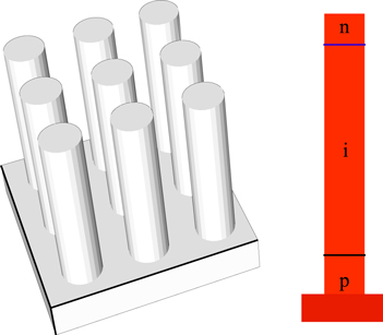
Figure 1. A schematic of an InP nanowire array with a p-i-n junction.
Download figure:
Standard image High-resolution imageFirst, a gradient in the doping concentration of the top segment is used for creating an electric field that deflects the photogenerated holes away from the top contact. However, the performance of this design is limited by the increasing recombination losses with increasing carrier concentration due to the increased doping. In the second design, instead of InP we use GaP for the top n segment, as it has a higher band gap. Due to the larger and more indirect band gap, a much smaller number of electron–hole pairs is generated in the top segment. Consequently, a much smaller amount of photogenerated holes can diffuse into the top contact. With this design, thanks to the weaker photogeneration in the top segment, we can allow for a much longer top segment without a detrimental drop in the short-circuit current. The possibility of using a longer top segment could also facilitate the fabrication and contacting of nanowire array solar cells. We believe that these design schemes for managing minority carriers in nanowire photovoltaic devices open the door to higher performance in both single-junction and multi-junction nanowire array-based solar cells.
2. Theoretical tools: opto-electronic modeling
In the opto-electronic modeling of the short-circuit current, we find solutions to the absorption of incident photons and the consecutive separation and transport of the resulting electrons and holes. The optical response of the nanowire array is solved using the Maxwell equations, and the electron–hole transport in the nanowires is solved using the drift-diffusion formalism. We use the finite element method for this numerical analysis.
2.1. Optics modeling and optical generation function G(r)
We solve for the diffraction of light in the nanowire array using the Maxwell equations [23, 24]. In this modeling, we include the three-dimensional geometry of the nanowire array. The optical response of the constituent materials is described by their complex valued refractive indexes, and we use tabulated values for InP and GaP [25], respectively. Note that for simplicity we neglect possible variations in the refractive index due to doping in the n and p segments. Such effects are expected to cause only a minor impact on the resulting short-circuit current for the doping concentrations considered in this study.
We solve for normally incident light, that is, for incident light parallel to the axis of the nanowires, and we use periodic boundary conditions with one nanowire per unit cell. As a result, we obtain the electric field E(r) throughout the system. From this electric field, we can calculate the local absorption of incident photons in the nanowires and the substrate, which is proportional to Re(n(r))Im(n(r))|E(r)|2 [2]. For a given incident intensity spectrum I(λ) we can then calculate G(r), the number of electron–hole pairs photogenerated per unit volume per unit time. This G(r) enters the drift-diffusion modeling for the electron–hole transport (equation (1)). For the calculation of G(r), we use circular polarized light and an incident intensity given by the AM1.5D solar spectrum (ASTM G173-03) with a total input power of 900 W m−2.
2.2. Drift-diffusion modeling
We solve the electron–hole transport with the drift-diffusion formalism (see, e.g., ref. [26]):
Here, ε is the (static) dielectric constant, q is the elementary charge, μn/p is the electron/hole mobility, n(r)/p(r) is the electron/hole concentration, φ(r)/φn(r)/φp(r) is the electrostatic potential/electron quasi-Fermi potential/hole quasi-Fermi potential, Nd/a(r) is the concentration of ionized donors/acceptors, R(r) is the net recombination rate and G(r) is the optical generation rate defined in section 2.1. For R in the bulk of the nanowire, we use:
where A/B/C is the recombination coefficient of the SRH/radiative/Auger recombination, and ni is the intrinsic carrier concentration [26, 27]. Here, we assume that the electron and hole concentrations are equal to ni in the case where the Fermi level coincides with the trap level responsible for SRH recombination, and we assume an equal SRH lifetime for electrons and holes [28]. Regarding the Auger recombination rate, the same coefficient C is assumed for electrons and holes. Since it is very challenging to include wave-optical effects in light emission, and as we focus on the short-circuit current, we neglect radiative recombination in this study. That is, we use B = 0 in equation (2). See online supplementary data section S1, however, for a discussion of the possible effects of radiative recombination. The surface recombination, at the surface of the nanowire, is included through the term:

where vsr is the surface recombination velocity [29].
In the drift-diffusion equations, the carrier concentrations n and p are calculated by:
where kb is the Boltzmann constant, me/h* is the effective mass of electrons/holes,  is the reduced Planck constant, and EF0 is the Fermi level at zero bias voltage and zero optical generation:
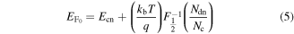
where Ndn is the ionized donor concentration which equals the n doping level and Ecn is the conduction band edge, both calculated at the n-type contact.
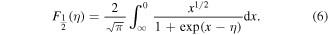
In equations (4) and (5), the functions F1/2 and  are, respectively, the ½ order Fermi integral and its inverse function:
In addition, the band edges are calculated as


where ΔVBO(r) = VBO(r)-VBOInP with VBOInP the value for InP, and Eg (r) is the band gap.
The specific values for the parameters used in the drift-diffusion modeling are listed in table 1. Note that for simplicity in the modeling, we do not include doping-induced band gap narrowing, or strain-induced band offset in the lattice mismatched heterostructures like the GaP/InP system in section 3.5. Strain effects are only important close to the interface between InP and GaP, and the strain relaxes away from the interface. For the length of the GaP segment we use in section 3.5, the strain is negligible at the top.
Table 1. The parameters used in the drift-diffusion modeling [30, 31], unless explicitly stated otherwise in direct connection to the presented results.
| Parameters | InP | GaP |
|---|---|---|
| Dielectric constant (ε) | 12.5ε0 | 11.1ε0 |
| Surface recombination velocity (vsr) | 200 cm s−1 | 2 × 105 cm s−1 |
| Shockley–Read–Hall recombination coefficient (A) | 107 s−1 | 107 s−1 |
| Auger recombination coefficient (C) | 9 × 10⁻³¹ cm6 s−1 | 10−30 cm6 s−1 |
| Electron mobility (μn) | 5400 cm2V−1 s−1 | 250 cm2V−1 s−1 |
| Hole mobility (μp) | 250 cm2V−1 s−1 | 150 cm2V−1 s−1 |
| Band gap | 1.34 eV | 2.26 eV |
| Valence band offset (VBO) | −1.27 eV | −0.94 eV |
Regarding the geometry used in this drift-diffusion modeling, we consider a single nanowire on top of a substrate. Note, however, that the G(r) is calculated for the nanowire array. We place an ohmic contact at the top of the nanowire, and in the drift-diffusion modeling, the substrate has a lateral size equal to the unit cell size of the array and a depth of 300 nm. We also placed an ohmic contact at the bottom of the substrate and ascertained that its thickness did not affect the resulting short-circuit current. Unless otherwise stated, we used a 100 nm long n segment and a 300 nm long p segment in the modeling, and both segments have an ionized doping concentration of 1018 cm−3.
The ohmic boundary condition at the short-circuit current is defined as:
where V0 is
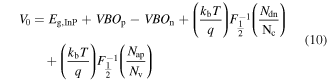
where Nap/dn is the p/n doping level at the p/n contact and VBOp/VBOn is the valence band offset at the p/n contact.
2.3. Spatially resolved internal quantum efficiency (SIQE)
For a more detailed analysis of the charge separation mechanism within the nanowires, we used the spatially resolved internal quantum efficiency (SIQE). The SIQE is given by the spatially resolved probability S(r) of an electron–hole pair, injected at r, to contribute an elementary charge to the short-circuit current at a zero bias voltage. Practically, we calculate S(r) by using a generation rate density of GSIQE = 1028 m−3 s−1 in a cubic box of volume VSIQE with a 10 nm side length, centered at r (we ascertained that the resulting SIQE did not vary noticeably with varying GSIQE around this value); that is, VSIQE = (10 nm)3. Next, using the drift-diffusion equations we calculate the short-circuit current Isc,SIQE that flows through the nanowire due to this injection. Finally, we obtain the SIQE as: S(r) = (1/q) Isc,SIQE/(GSIQEVSIQE). Note that a similar SIQE is used in ref. [32] for the analysis of silicon nanowire photovoltaic devices.
3. Results and discussion
3.1. Factors limiting the short-circuit current from Jsc,max = 31 mA cm−2
In wave-optics, the absorption performance of the nanowire array depends on the nanowire diameter, the nanowire length, and the array pitch [13]. When considering the absorption of sunlight, we typically look at the short-circuit current Jsc. This current results from the absorption of photons and the consecutive separation of the photogenerated electrons and holes over the p-i-n junction. For the 900 W m−2 direct and circumsolar AM1.5D solar spectrum, we obtain an upper limit of Jsc,max = 31 mA cm−2 for InP with a band gap Eg = 1.34 eV by assuming that each incident photon with an energy of Eph > Eg is absorbed, and that each photogenerated electron–hole pair contributes to the short-circuit current. Below, we consider the two effects that decrease Jsc from Jsc,max: (1) less than 100% absorption and (2) less than 100% probability of separating the photogenerated charges over the p-i-n junction.
3.2. Geometry dependence of the short-circuit current
Both modeling [33] and measurements [34] have shown that nanowire arrays can absorb incident light that would travel between the nanowires in a ray-optics description [33]. This absorption beyond the geometrical cross-section of each nanowire occurs due to the delocalized wave-nature of light [35]. By optimizing the geometry of the array, the nanowires can absorb almost all of the incident light, incident on the whole nanowire array with energy above the band gap energy of the semiconductor [13]. Therefore, the short-circuit current has the potential to approach Jsc,max.
For nanowire arrays, the short-circuit current shows diameter-dependent peaks [13] due to diameter-dependent absorption resonances in the nanowires. The diameter that optimizes the absorption depends on the band gap Eg of the nanowire material. For InP with Eg = 1.34 eV, the smallest diameter that optimizes the absorption performance is D = 180 nm. We fix D = 180 nm throughout this study, and we choose a nanowire length of L = 1400 nm to match the experiments [2].
In figure 2(a), Jsc is plotted as a function of the remaining free parameter, the pitch of the square array. In the drift-diffusion modeling (solid line in figure 2(a)), we find a maximum value of 25.8 mA cm−2 when the pitch is 330 nm. We also find Jsc = 24.2 mA cm−2 for the pitch P = 470 nm, which has been used in previous experiments for InP nanowire arrays [2]. Both these short-circuit values are lower than the upper limit Jsc,opt from absorption modeling (dashed line in figure 2(a)), which predicts an upper limit of Jsc,opt = 28 mA cm−2 for Jsc assuming a 100% contribution from all the photogenerated carriers to the current. In contrast, drift-diffusion modeling includes loss mechanisms that lead to a less than 100% probability of splitting the photogenerated electron–hole pairs over the p-i-n junction.

Figure 2. (a) The short-circuit current as a function of the nanowire array pitch. Here, we show the absorption limited Jsc,opt (dashed line) as well as the Jsc from the drift-diffusion modeling (solid line). Note that for Jsc,opt we assume a 100% probability for each photogenerated electron–hole pair to contribute to the short-circuit current. In contrast, in the drift-diffusion modeling we include varying recombination mechanisms that can decrease this probability. The nanowires are 1400 nm long with a 100 nm long n-doped top segment and a 300 nm long p-doped bottom segment. The ionized doping concentration is 1 × 1018 cm−3 for both the n and the p segment. (b) The optical generation rate G(r) in one nanowire of the array in figure 1.
Download figure:
Standard image High-resolution imageTo better understand the absorption properties of the nanowires, we turn to the spatial distribution of the optical generation rate in the nanowire (figure 2(b)). First, we find a radial dependence where the optical generation rate peaks between the center and the surface of the nanowire. We assign this radial profile to the radial pattern of the optical eigenmodes of the nanowire array [23, 24]. Next, we find a very strong dependence of the generation as a function of the position along the axis of the nanowire. For example, 85% of the generation occurs in the top half of it. Also, the maximum generation rate in the nanowire is two orders of magnitude higher than in the substrate. This strong generation in the top part of the nanowires indicates that it is very important to maximize the probability of extracting photogenerated carriers from this segment. Thus, in the next subsection we investigate how the design of the p, i, and n segments affects this extraction probability.
3.3. Doping segment length dependence
To investigate the possible effect of the design of the p, i, and n segment on the short-circuit current, we varied the segment lengths for the above fixed nanowire length L = 1400 nm. In this way, the photogeneration inside the nanowire does not change. Thus, any variation in Jsc originates from variations in the efficiency of splitting electron–hole pairs over the p-i-n junction.
Figure 3(a) shows the short-circuit current when the n and p segment lengths are varied. We varied the p segment length for a fixed n segment length of 300 nm (blue line in figure 3(a)). Similarly, we varied the n segment length for a fixed p segment length of 300 nm (black line in figure 3(a)). We find that Jsc is much more sensitive to a variation in the length of the top n segment than to a variation in the length of the bottom p segment. An increase of the bottom segment length from 25 nm to 900 nm decreases the Jsc by just 2.7 mA cm−2, from 21.0 mA cm−2 to 18.3 mA cm−2. In contrast, Jsc decreases by 16.5 mA cm−2, that is, by more than 60%, when the n segment length is increased by a similar amount. Note that such a strong dependence on the length of the top n segment is to be expected from the much stronger optical generation rate in the top part of the nanowire rather than in the bottom part (figure 2(b)).

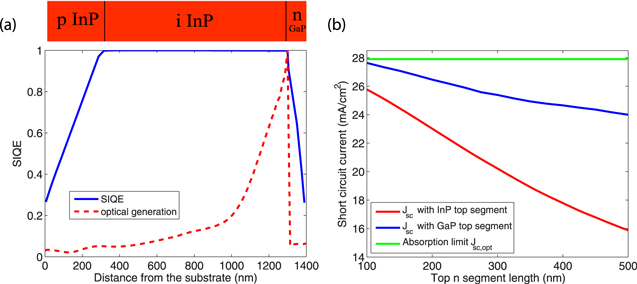
Figure 3. (a) Jsc as a function of n and p segment length for InP nanowires of diameter D = 180 nm and length L = 1400 nm, placed in a square array of pitch p = 330 nm on top of an InP substrate. To vary the n (p) segment length, the p (n) segment length is kept constant at 300 nm. (b) The spatial internal quantum efficiency S(r) in a nanowire of the array considered in (a), as a function of position along the axial direction. Here, we consider three different n segment lengths: 100, 300, and 500 nm (solid lines). We also show the normalized optical generation rate (dashed red line). Before the normalization, the generation rate was integrated over the cross section of the nanowire. A schematic of a nanowire with a 300 nm long top n segment is placed at the top of this plot to aid the eye, and the multi-colored arrow indicates the incidence direction of the light.
Download figure:
Standard image High-resolution imageTo obtain a better, quantitative, understanding of this strong dependence on the top n segment length, we studied the SIQE (solid lines in figure 3(b)) to vary the length of the n segment. That is, we studied the spatially resolved probability S(r) of splitting electron–hole pairs over the p-i-n junction (see section 2.3 for technical details). To aid the analysis, we also show the optical generation rate in the nanowire (dashed red line in figure 3(b)). First and foremost, we find a rapid decrease in the SIQE when moving the n segment from the edge of the i segment toward the top contact. We find a similar drop in the p segment when moving down, away from the edge of the i segment. In contrast, the SIQE is close to 100% in the i segment. This drastically different behavior originates from the existence of an electric field in the i segment, which is lacking in the n and p segment. In the i segment, the electric field splits the electron and the hole rapidly and efficiently in opposite directions, leading to a high SIQE. In the n and p segment, the electron and the hole diffuse instead. For example, if a hole generated in the n segment, which is the minority carrier, diffuses into the i segment, it will be swept toward the p side by the electric field and contributes to the current over the p-i-n junction. However, if the hole diffuses into the ohmic top contact, it contributes to current leakage and recombines in the contact.
The probability of the hole diffusing from the n segment into the i segment depends on the distance to the i segment and the distance to the ohmic top contact. Therefore, the SIQE decreases from close to 100% to close to 0% when the photogeneration position shifts from the edge of the i segment to the edge of the ohmic contact. Note that a similar behavior/drop has recently been observed in the electron-beam-induced current measurements of individual, as-grown nanowires [1]. Thus, we believe that our modeling accurately represents the loss mechanism in short-circuit currents in such experiments.
The number of holes that are photogenerated in the top n segment increases on increasing the length of the n segment. Hence, on increasing the segment length, more holes are available for diffusion to the top contact, leading to an increasing drop in Jsc in figure 2(a). Furthermore, the optical generation rate is high in the topmost 300 nm of the nanowire (dashed red line in figure 3(b)). Therefore, an increase of the n segment length from 25 nm to 300 nm causes a rapid drop in Jsc (marked by region 1 and region 2 in figure 3(a)). When the n segment length is further increased from 300 to 1100 nm, the decrease in Jsc is slower (marked by region 3 and region 4 in figure 3(a)), since the optical generation rate is lower here than in the topmost 300 nm.
Thus, a shorter n segment length leads to a higher Jsc by decreasing the number of holes that can diffuse into the ohmic top contact. The effect of increasing Jsc on decreasing the top n segment length has already been reported from the experiments in [2], although it has not been assigned to the diffusion of minority carriers into the top contact. Nevertheless, in the experiments, a drastic decrease in the n segment length can become impractical due to problems in contacting nanowires with a short top segment [2]. Below, in order to maximize Jsc, we present two alternative designs for limiting the diffusion of holes into the top contact.
3.4. Gradient doping to prevent holes from reaching the top contact
Here, in order to maximize Jsc, we discuss the potential of using a gradient in the doping profile in the n segment to prevent photogenerated holes from reaching the top contact. Note that such a doping scheme is often used at the bottom side of planar solar cells in order to reduce the diffusion and consecutive loss of minority carriers into the back contact [36].
We consider a linear increase in the doping concentration from 1 × 1018 cm−3 at the edge of the i segment to ncontact at the edge of the ohmic contact. Here, we assume that the dopants are fully ionized. This gradient introduces an electric field to the n segment, which prevents the holes from reaching the top contact. In terms of the band diagram, this doping profile bends the valence band edge down toward the ohmic contact.
The Jsc is shown in figure 4(a) as a function of the doping concentration increase from the i segment to the top contact. We find that Jsc increases initially with an increasing gradient in the doping concentration. When ncontact increases from 1 × 10¹⁸ to 1.5 × 1019 cm−3, Jsc increases from 25.8 mA cm−2 to 27.1 mA cm−2, that is, by 5%.

Figure 4. (a) Jsc as a function of ncontact, the doping concentration in the 100 nm long top n segment from the interface to the top contact. The doping concentration increases linearly to ncontact from the value of 1018 cm−3 at the interface between the n and the i segment. (b) The minority carrier current to the top contact and the recombination, translated into equivalent current loss, as a function of ncontact.
Download figure:
Standard image High-resolution imageTo explain the shape of the curve shown in figure 4(a), we show in figure 4(b) the different loss current mechanisms, again, as a function of the doping concentration increase. As expected, the minority carrier current, that is, the hole current, to the top contact decreases monotonously with an increasing doping gradient, that is, with an increasing ncontact (dashed line in figure 4(b)). However, when the ncontact > 1.5 × 1019 cm−3, the further increase actually leads to a decrease in Jsc (figure 4(a)). This decrease originates from the increasing recombination losses in the n segment due to the increasing carrier concentration with increasing doping.
Initially, when 1 × 10¹⁸ < ncontact < 1 × 1019 cm−3, surface recombination is the dominant recombination mechanism, even in the case of the low surface recombination velocity of 200 cm s−1 used here (see online supplementary data section S2 for a discussion of the effect of increasing surface recombination velocity and the online supporting information section S1 for a discussion of the possible effects of radiative recombination). In this case, the total recombination rate is several orders of magnitude lower than the corresponding minority carrier leakage into the top contact, as seen in figure 4(b). Thus, for a low doping level, the major loss mechanism in Jsc is the diffusion of holes into the top contact.
However, with an increasing ncontact, Auger recombination, which scales as the carrier concentration to the third power, in contrast with the surface recombination that scales as the carrier concentration to the first power, sets in (see solid line in figure 4(b)). Auger recombination becomes significant when ncontact = 1019 cm−3 and increases sharply for a higher ncontact. For example, for ncontact = 2 × 1019 cm−3, the Auger recombination amounts to 2% of the optical generation rate in the whole nanowire and starts to limit Jsc noticeably. Note that the high doping level does not cause a net Auger recombination in itself, but induces a high Auger recombination velocity for the optically generated holes, which strongly reduces the benefit of gradient doping at very high doping levels.
Thus, by using a gradient doping profile in the top n segment, we can prevent the minority carriers—that is, the holes—from reaching the top ohmic contact. With an increasing doping gradient, we deflect the minority carriers away from the contact more and more efficiently. However, at the same time, we open ourselves up to Auger recombination of the photogenerated carriers, which decreases the overall current. Note that when such a gradient doping profile is used at the back side of a planar solar cell [36], we do not expect similar problems with increased recombination, since the photogeneration rate is expected to be low on the bottom side of the solar cell.
3.5. High band gap material for the top n segment
To avoid the increased recombination losses introduced by the gradient doping profile above, we consider here a design with a semiconductor heterostructure. Our idea is to use a semiconductor with a higher band gap for the top n segment, in which only a small amount of holes is generated. In this way, only a small amount of holes can diffuse into the top contact. After consideration of both the band structure [37] and growth possibilities [38], we selected GaP, which has an indirect band gap, to be used for the n segment. We keep the total length of the nanowire at the previously chosen L = 1400 nm. We have calculated the photogeneration rate for the case of a GaP top segment (dashed line in figure 5(a)), which should be compared to the case of an InP top segment in figure 3(b). The optical generation rate in this GaP top n segment is 2.3 mA cm−2, which is only 9% of that in the InP i segment below. At the same time, we find a charge separation of close to 100% in the i segment—that is, SIQE ≈ 100% (solid line in figure 5(a)). The concentration of photogeneration into the i segment with an SIQE ≈ 100% leads to a high Jsc, with values close to the absorption limited Jsc,opt.
Figure 5. (a) The SIQE, the spatially resolved internal quantum efficiency S(r), and the cross-section-integrated and normalized optical generation rate G(r) in an InP nanowire of the array. The nanowires are 180 nm in diameter and 1400 nm in length, and they have a 100 nm long GaP top n segment on top of an intrinsic InP segment, which is in turn on top of a 300 nm long InP bottom segment. The nanowires are placed in a square array 330 nm in pitch on top of an InP substrate. (b) The dependence of the Jsc on the n segment length for the nanowire array geometry in (a); here, the nanowires have either a GaP top segment (blue solid line) or an InP top segment (red solid line). For comparison, we show the absorption-limited short-circuit current Jsc,opt for the case of an InP top segment (dashed line), where we assume that each photogenerated electron–hole pair contributes to the current.
Download figure:
Standard image High-resolution image
Finally, when we compare the Jsc for varying n-segment length (figure 5(b)), we find much higher current levels with the GaP top segment than with the InP top segment. For a 100 nm long GaP segment, we reach a short-circuit current of 27.6 mA cm−2. This current level is very close to the above-stated absorption limited Jsc,opt = 27.9 mA cm−2 in a 1400 nm long InP nanowire, when all the photogenerated carriers are extracted as current. Note that the overall absorption in the nanowire tends to decrease with an increasing length of GaP segment. For example, for a GaP segment of 500 nm in length, the drop in the overall absorption is equivalent to a photocurrent of 1.7 mA cm−2 (see supplementary data section S3).
When the GaP segment length is increased from 100 nm to 500 nm, the current drops from 27.6 to 24.0 mA cm−2. In contrast, a similar increase in the n segment length when using InP for the top segment causes a much larger drop—from 25.7 to 15.9 mA cm−2. Thus, for the 500 nm long top segment, the use of GaP gives a 50% higher short-circuit current. In this way, with the GaP top segment, we can allow for a relatively long top segment without losing current detrimentally.
4. Conclusion
Through modeling, we analyzed the short-circuit current in an InP nanowire array solar cell with an axial p-i-n junction in each nanowire. We assumed an ohmic contact on top of the top n segment, as is conventionally done in the fabrication of nanowire array solar cells. In such a structure, the photogenerated minority carriers in the n segment, that is, the holes, can diffuse readily into the close-lying top contact. Indeed, if a photogenerated hole diffuses into the top contact, it recombines without contributing to the short-circuit current. If the hole instead manages to diffuse into the i segment, it is swept to the p side by the built-in electric field, which leads to a charge separation over the p-i-n junction and consecutively to a contribution to the short-circuit current.
By reducing the length of the top n segment, we reduce the number of photogenerated holes there. Therefore, we limit the number of photogenerated holes lost due to diffusion into the top contact, and the short-circuit current increases. However, a drastic decrease in the top segment length can lead to issues with contact fabrication. A planarized contacting scheme is typically used for the top contact. Due to the standard deviation in both the nanowire length and the contact layer planarization, a part of the side wall of the top segment is also typically contacted, and the extent of this sidewall contacting varies from nanowire to nanowire. With a short top segment, it becomes impractical to contact each nanowire without forming a contact to the i segment in some nanowires. Therefore, we proposed two alternative designs to reduce hole diffusion into the top contact.
In the first design, we increased the doping concentration in the n segment toward the top contact. Such a gradient in the doping profile leads to an electric field in the n segment which prevents the holes from reaching the top contact. However, we found that the performance gain with this approach was limited by the increasing recombination losses due to the increasing carrier concentration with increased doping.
In the second design, we replaced the InP in the n segment with GaP, which has a higher band gap. Due to the higher indirect band gap of GaP, the number of photogenerated holes decreases dramatically in the top segment. Therefore, a much lower number of holes can diffuse from the top segment into the top contact. With this approach, we found that a considerably larger top segment length could be allowed for, without any detrimental loss to the short-circuit current. At the same time, with such a long top segment, we expect that we will be able to allow for a larger standard deviation in both the nanowire length and the height/thickness of the planarized contact layers.
In principle, this design could also be applied to a tandem cell with GaInP/InP nanowires on top of a Si substrate cell, as well as to a GaInP(GaAsP)/InP or GaInP(GaAsP)/GaAs nanowire tandem solar cell.
Our study provides important guidelines for optimizing the short-circuit current in nanowire array solar cells. We believe that the optimization of short-circuit current can be used as an initial step in the optimization of nanowire array solar cell efficiency. Such efficiency optimization requires a study of the full IV characteristics, since the output power of the solar cell is maximized at a non-zero output voltage Vmax.
Acknowledgments
This work was performed within NanoLund and received funding from the People Programme (Marie Curie Actions) of the European Union's Seventh Framework Programme (FP7-People-2013-ITN) under the REA grant agreement no. 608153, PhD4Energy, and the European Union's Horizon 2020 research and innovation programme under grant agreement no. 641023, NanoTandem. This article reflects only the author's view and the funding agency is not responsible for any use that may be made of the information it contains. Kivisaari wants to express his gratitude to the Nokia Foundation and the Finnish Cultural Foundation for financial support.