

Abstract
We propose a compact, wideband terahertz and infrared absorber, comprising a patterned graphene sheet on a thin metal-backed dielectric slab. This graphene-based nanostructure can achieve a low or negative effective permeability, necessary for realizing the perfect absorption. The dual-reactive property found in both the plasmonic graphene sheet and the grounded high-permittivity slab introduces extra poles into the equivalent circuit model of the system, thereby resulting in a dual-band or broadband magnetic resonance that enhances the absorption bandwidth. More interestingly, the two-dimensional patterned graphene sheet significantly simplifies the design and fabrication processes for achieving resonant magnetic response, and allows the frequency-reconfigurable operation via electrostatic gating.
Export citation and abstract BibTeX RIS
Introduction
Ever since graphene was first isolated by Novoselov et al in 2004 [1], there have been numerous and significant studies investigating its physical properties and applications in various fields of electronics, photonics, mechanics, biology and chemistry [1–4]. Graphene is a two-dimensional (2D) structure formed by carbon atoms arranged in a hexagonal lattice, and shows ultrahigh carrier mobility, stable thermal properties, and carrier-density-dependent sheet conductivity with a possible plasma frequency in terahertz (THz) and infrared (IR) regimes [1–6]. Graphene has been shown to support propagation of tightly confined surface electromagnetic waves at its interface with a dielectric, so called 'graphene surface plasmon polaritons (GSPPs)'. On a high-quality graphene monolayer, GSPPs have longer propagation lengths than surface plasmon polaritons (SPPs) generated at the metal/dielectric interfaces [7, 8] at THz or IR frequencies. Moreover, their characteristics can be readily tuned through electronic or chemical doping, which shift the plasma frequency of graphene. It has been experimentally demonstrated that below the interband transition threshold ( generally valid for doped graphene at far-/mid-IR, the complex intraband conductivity of graphene can be modeled as
 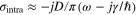 [
[![$\Omega ]$](https://content.cld.iop.org/journals/0957-4484/26/16/164002/revision1/nano510178ieqn3.gif) [8].
[8].  the Drude weight of graphene,
  is the angular frequency of light,
  is the Fermi energy,
  is the phenomenological scattering rate that accounts for plasmon loss,
  is the electronic charge, and
  is the reduced Planck constant. Due to the need for making tunable, compact-size, broadband photonic and optoelectronic devices, graphene plasmonics has become an extremely promising paradigm for versatile THz/IR nanodevices. Recently, several THz/IR graphene-based devices have been proposed, including antennas [9–16], phase shifters [17], plasmonic waveguides [18] and interconnects, transformation-optics devices [19], cloaking devices [20–22], absorbers [23–25], sensors [26], modulators [17], couplers [27], and photomixing frequency synthesizers [28]. The realization of these functionalities at the nanoscale, with the potential of being frequency-reconfigurable, may pave a practical way to sensing, communication, and information processing with carrier frequencies up to the THz and even IR frequencies [10, 29].
Recently, graphene and graphene-based metamaterials have been proposed to realize the near-complete absorption of electromagnetic radiation at the THz and IR frequencies, in hopes of improving the size and performance of conventional bulk absorber configurations used at radio frequencies and microwaves [23–25]. The most important advantage of graphene-based absorbers is that by electronically gating the graphene structures, one may significantly tune the absorption peaks. The compact THz/IR absorbers made of the one-atom-thick graphene may be applied to diverse applications in selective emitters, sensors, spatial light modulators, IR camouflage, wireless communication, and thermophotovoltaics [20, 30, 31].
In this work, we propose an ultracompact THz/IR absorber based on graphene metaferrites shown in figure 1(a), with an enhanced absorption bandwidth. Different from typical magnetic metamaterials composed of densely-packed split-ring resonators or spiral resonators [32–37], as shown in figure 1(b), the proposed metaferrite consists of only a nanostructured graphene sheet placed on an ultrathin metal-backed dielectric slab, as shown in figure 1(c). The backside metal serves as the gate electrode for shifting the Fermi level of graphene, thereby achieving the tunable electromagnetic response. For graphene sheets with specific geometries, e.g. nanopatch array [21, 38], the dual capacitive–inductive properties may be obtained from the geometry-yielded capacitance and the kinetic inductance of graphene implied from the plasmonic effect. A dual-reactive graphene metascreen has been demonstrated to realize THz cloaks that are effective in hiding both dielectric and conducting objects at different operating frequencies [21]. We note that the similar dual reactive effect is found also in a grounded high-permittivity (high- ) slab at its resonances, as is in the conventional Salisbury absorbers [35]. Hence, by combining the dual-reactive properties of both graphene metascreen and grounded high- slab, a compact THz/IR absorber (figure 1(c)) with enhanced bandwidth can be achieved, thanks to additional poles introduced into the equivalent circuit of the system. In the following sections, we discuss the details of the design and the physical mechanisms of this graphene-based absorber with enhanced bandwidth.
Figure 1. Schematics for (a) a ground-backed magnetic metamaterial slab with the effective permeability  (b) and (c) are the practical realization of (a) with bulk metamaterial and ultrathin metascreen technologies, respectively.
Download figure:
Standard image High-resolution imageMechanism of electromagnetic complete absorption
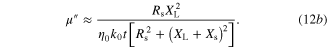
In this section, we discuss the physics of ultra-compact absorbers realized with extreme material properties, i.e. near-zero permeability. According to the optical theorem, as the scatterer interacts with the incident fields, the power depleted from the incident fields is the sum of the absorbed and scattered powers, i.e.  This power balance is fundamentally restricted by the energy conservation followed by the causality. The time-averaged absorbed power is calculated from the surface integral of the inward flowing flux of the Poynting vector of the total field through the surface S surrounding the scatterer [36]

where { and {
and { are the incident and scattered fields, respectively. Similarly, the time-averaged scattered power, which represents the re-radiated power from the scatterer, is the surface integral of the outward flowing flux of the Poynting vector of scattered fields

The total incident power flowing through the surface S is zero

From equations (1)–(3), the total extracted power (power extinction) is given by only the cross terms

The forward scattering sum rule is also valid for compact planar absorbers, for which the scattered power  is the sum of the backward scattered (reflected) power
  and the power in the scattered part of the transmitted field (the difference between the total field and incident field in the forward direction)
 and
and  are reflection and transmission coefficients of the compact planar absorber, respectively. The total scattered power
  can be expressed as

The absorbed power  is the difference between the incident power and the sum of reflected and transmitted power
  as
as

Assuming that there are no grating sidelobes, the power extinction  is given by

This can be seen as the optical theorem for infinite 2D structures, such as metascreens or absorptive films. From equations (5)–(7), it is interesting to note that when the forwardly scattered power represents the total scattered power (no backwardly scattered (reflected) waves), total absorption of the incident radiation can be achieved. In this situation, the scattered power equals the absorbed power, namely,  which is somehow similar to the conjugated matching condition in the equivalent Thevenin or Norton circuit. The 100% absorption occurs only for an asymmetric system, such as a metal-back thin absorptive slab or a surface that combines both electric and magnetic dipoles [39, 40]. For instance, electric and magnetic dipole arrays at the metascreen would radiate symmetric and anti-symmetric electric fields on either side of the metascreen, respectively [39, 40]. The anti-symmetry introduced by magnetic dipoles enables the complete cancellation of incident fields in the forward direction without generating any backwardly propagating wave, thereby achieving the perfect absorption [39, 40]. A metal-backed magnetic-near-zero (MNZ) metamaterial slab, typically composed of split-ring resonators or spiral resonators (see figure 1(b)), presents an asymmetric system for making a perfect absorber [32–37]. For ultrathin, metal-backed MNZ absorbers (within the quasi-static limit of
  the permeability
  has an analytical expression [37]


 and
and  are the wave number and the permeability of free space, respectively, and
  is the thickness of the metamaterial slab. This asymmetric absorber configuration may easily achieve the zero backward scattering (i.e.
  and a large forward scattering (i.e.
  with
with  and
and  On the other hand, if we use a symmetric design, such as a suspended resistive film with optimal sheet impedance
  (
( is wave impedance of free space) or an epsilon-near-zero (ENZ) thin-slab with optimal permittivity
  only half of incident radiation is absorbed and half is re-radiated by the surface. Due to the symmetric geometry and the negligible thickness of a resistive film or an ENZ thin-slab, the induced surface current would re-radiate symmetric fields to both sides of the sheet, namely
  In this scenario, the maximum absorbed power is only 50% of the incident power, with
  and
and 
Graphene metaferrite and its equivalent circuit model
Here, we propose a THz and IR metaferrite in figure 1(c), which is formed by a graphene-nanostrip metascreen at z = 0, separated from the ground plane by a dielectric slab. Consider a thin grounded (short-circuited) metaferrite slab with thickness  and permeability
  as shown in figure 1(a). The surface impedance at the interface between air and the metaferrite is [41]

A metascreen made of planar arrays of subwavelength inclusions can be modeled with its average sheet impedance  which neglects the higher-order Floquet harmonics. The load impedance of the dielectric substrate backing the metascreen is
  where
where  and
and  are the impedance and wave number of the dielectric slab, respectively. By equating the surface impedance of a grounded metaferrite in figure 1(a) to that of the graphene nanostructures in figure 1(c)

and taking the quasi-static limit, i.e. 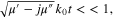 one may obtain the equivalent real and imaginary parts of permeability of the metaferrite
Therefore, a metaferrite with the desired magnetic property can be obtained with the physically realizable geometry in figure 1(c). The material dispersion of metaferrite is determined by the sheet reactance  and the sheet resistance
  of the metascreen, which depends on the geometry and the plasma frequency of graphene inclusions, and by the type of substrate that affects the load reactance
Here, we use the simplest possible metascreen consisting of a 2D graphene nanostrip array. Consider a uniform plane wave normally incident on this metascreen, where the electric fields are parallel to the nanostrips as  Due to the periodic nature of the nanostrip arrays, we may present the reflected and transmitted fields by an infinite summation of Floquet space harmonics:
where  and
and  If the periodicity of nanostrips a is much smaller than the free space wavelength
  (i.e.
(i.e. 
 has a negative imaginary value and the fields of grating lobes decay exponentially away from the metascreen. In this scenario, only the reflection coefficient R and transmission coefficient T are of practical interest. We note that the nanopatch array is another interesting possibility for removing the polarization selectivity. The sheet impedance of patch array is, however, identical to that of the strip array, provided that the patch dimensions and the gap are subwavelength [42, 43]. The infinitesimally-thin strip-array geometry provides a capacitance [42–45] as:

where  is the relative permittivity of substrate,
  and
and  are respectively the period and gap of graphene nanostrips,
  and
and  are the angular correlation functions corresponding respectively to TM-
 ![$\left[ \left( {\bf k}\times {\bf E} \right)\cdot {\boldsymbol{\hat{z}}} =0 \right]$](https://content.cld.iop.org/journals/0957-4484/26/16/164002/revision1/nano510178ieqn60.gif) and TE- (
and TE- ( incident polarizations. We note that the excitation of SPPs in graphene nanostrips will contribute to an angle-independent kinetic inductance
  and a sheet resistance
  as [42–45]

The sheet resistance accounts for the plasmon energy loss in light of the intraband carrier scattering in graphene. In the equivalent circuit model in figure 2,  and
and  are in series with the geometry-yielded capacitance
  As a result, this graphene metascreen has a dual capacitive–inductive property, owning to the combination of kinetic inductance and geometric capacitance [21]. The sheet impedance of one-atom-thick graphene metascreen can therefore be modeled as:


Figure 2. Equivalent circuit model for metaferrite design given in figure 1(c).
Download figure:
Standard image High-resolution imageWe note that  and
and  are controlled by the Fermi energy of graphene
  which can be tuned by the chemical doping or the electrostatic gating, and therefore the sheet impedance of the graphene metascreen can be tuned over a wide range.
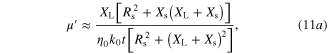
From equation (11), we know that the choice of substrate is also important for controlling the effective permeability of metaferrite. The load impedance of a grounded dielectric slab has a partial-fraction expression as
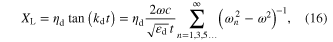
where  In the vicinity of the pole
  ,
, is obtained, in analogy to that of a LC parallel network with the expression:

where  and
and


A high- thin slab with thickness  may display a dual capacitive–inductive property around its first resonance. From the circuit model in figure 2, we may now re-write equation (11) and obtain the effective real and imaginary parts of permeability of a grounded metaferrite as:

This high-order LC system may clearly exhibit two distinct Lorentzian resonances. The first resonance (pole) occurs at
while the second resonance (pole) occurs at a higher frequency
Also, there exists a zero between two poles  which depends on the kinetic inductance and geometric capacitance of the graphene metascreen. By properly designing each lumped circuit elements in equations (13)–(14), and equation (18), an equivalent MNZ substrate with
  and
and  can be achieved between two resonant Lorentzian resonances in permeability. Once the effective permeability of metaferrite is extracted, the reflection
  and the absorptance
  can be calculated.
Results and discussion
We first analytically calculated the effective permeability and absorption of the proposed graphene-based metaferrites, and then conducted numerical simulations to verify the results. Figures 3(a)–(c) report the frequency dependencies of the equivalent permeability retrieved using equation (11) for the metaferrite in figure 1(c) with different metascreen geometries. Here a dielectric substrate with the relative permittivity = 25 (i.e. some compound oxides [46]) and thickness  is used. The Fermi energy of graphene is 0.7 eV and the intraband scattering rate of graphene
  For simplicity, we consider only the normally incident plane wave with the electric field polarized perpendicular to graphene nanostrips. We should note that since metaferrite absorbers can be made ultrathin, the absence of a requirement on a certain electrical distance can broaden the angular response (not discussed here).

Figure 3. Effective permeability for metaferrite in figure 1(c), with different geometries and material properties of graphene metascreens: (a) 

 and
and  (b)
(b) 

 and
and  (c)
(c) 

 and
and  (d)
(d) 

 and
and  (e)
(e) 

 and
and  (f)
(f) 

 and
and 
Download figure:
Standard image High-resolution imageIt is known from the equivalent circuit model in figure 2 that by properly designing the geometry of graphene metascreen: the period a and the gap g, as well as the thickness of the high- substrate, it is possible to achieve the single- or dual-band resonance. From figures 3(a)–(c), the Lorentzian resonances are seen around two poles  and
and  showing the interesting tunable multi-band resonances in the effective permeability. Figures 3(d)–(f) are similar to figure 3(c), but for graphene metascreens with different Fermi energies:
 and
and  It is observed that two magnetic resonances are tunable by electronically gating or chemically doping, which can considerably shift the Fermi level of graphene. For the proposed metaferrite designs,
  and
and  sourced from the graphene metascreen determines the 'zero' critical frequency
  while
while  and
and  sourced from the dielectric substrate, together with
 and
and  of metascreen, determine peaks of Lorentzian resonances (poles) and the effective permeability values of metaferrites. The large kinetic inductance of graphene plasmonic metascreen may significantly redshift the resonant frequency, thus squeezing the electrical size of metaferrite absorber
As can be expected, by bringing the first two poles ( and
and  close to the zero (
 through tuning the geometry, the plasma frequency (or EF) of graphene, and the thickness of the high- slab, a moderately broadband magnetic resonance can be obtained. Figures 4(a) and (b) report the effective permeability and the absorptance of graphene-based metaferrites with air (
 low- (
 i.e. silicon dioxide) high- dielectric slab (
 For making a fair comparison, the spacer thickness is fixed to
  for all cases, and geometries of metascreens on top of different dielectric slab are optimized to align the central frequency to 15 THz. The geometric and material parameters of graphene metascreen are: (1)

 and
and  for the high- dielectric slab, (2)

 and
and  for the low- dielectric slab, and (3)

 and
and  for the suspended graphene metascreen with an air gap.

Figure 4. (a) Effective permeability and (b) absorptance of the metaferrite absorber with enhanced bandwidth; here metaferrite absorbers comprising air gap (green dash–dot–dot line) and low- dielectrics slab are also presented for comparison. (c) Contours of absorptance for the metaferrite absorber in figure 4(a), varying the frequency of operation and the height of dielectric slab (normalized to the wavelength in free space). (d)–(f) are similar to (a)–(c), but with the operating frequency band centered at 9 THz.
Download figure:
Standard image High-resolution imageIt is evidently seen from figures 4(a) and (b) that the bandwidth of resonant magnetic response and absorption are significantly enhanced by using a high- dielectric slab, thanks to the dual-mode resonances in the proximity of central frequency. According to equations (20)–(21), poles and zeros on frequency responses are 
 and
and  which lead to the interesting broadband permeability resonance and absorption in figures 4(a) and (b). For a thin low- slab, the load impedance is purely inductive with
  In the absence of a dual-reactive substrate and therefore an extra pole in the circuit, only the narrowband magnetic resonance and absorption are obtained. Figure 4(c) reports the contours of absorptance for the metaferrite in figure 4(b) with the metal-backed high- dielectric slab, varying the operating frequency and the substrate height (normalized to free space wavelength). It is observed that the absorption bands are located at
  A relatively broad bandwidth is obtained at
  for which the first two poles,
  and
and  are closest to the zero
  It is also seen in figure 4(c) that for a thicker substrate (i.e.
 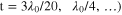 the bandwidth of absorption is narrower due to the separation of adjacent poles. To show the design flexibility of this metaferrite absorber, we also design an absorber with operating frequency centered at 9 THz. Figures 4(d)–(f) are similar to figures 4(a)–(c), but for a graphene-based metaferrite absorber operating at lower frequencies. The geometric and material parameters of graphene metascreen are: (1)

 and
and  for the high- dielectric slab and (2)

 and
and  for the suspended graphene metascreen with an air gap; the dielectric slab and the air gap have the dimension
  For the high- slab case, poles and zero calculated from equations (20)–(21) are:
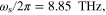
 and
and 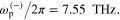 It is clearly seen from figures 4(d)–(f) that the absorption bandwidth can be enhanced by using a high- dielectric slab, and the design frequency can be readily changed by adjusting the geometric and material properties of graphene metascreen and the dielectric slab. We should note that the dual resonance in effective permeability may be used to realize cloaking devices [21], with dual and/or enhanced bandwidth, which will be discussed elsewhere.
Here, we also calculate the effective permeability and the absorptance for a single graphene sheet on a grounded high- dielectric substrate, as shown in figure 5. The inset of figure 5(a) shows its equivalent circuit model. In figure 5(a), it is seen that without nanopatterning the graphene, it displays a single resonance with its depth modulated by graphene's Fermi energy. Figure 5(b) reports the corresponding absorptance of figure 5(a), showing a reduced bandwidth compared to the graphene-nanostrip metaferrite. Since the extra pole yielded by the capacitance of metascreen is not presented, a pure graphene monolayer cannot maintain a flat absorption band. Besides, it requires an unrealistically high Fermi energy to reach the comparable absorption peak with the metaferrite in figure 4.

Figure 5. (a) Effective permeability and (b) absorptance of a graphene monolayer (GM) deposited on the same substrate in figure 4(a); the Fermi energy of graphene is varied. The inset of (a) shows the equivalent circuit model of a graphene monolayer on a grounded dielectric slab. In (b), the gray dashed line presents the absorptance of the broadband metaferrite in figure 4(b) (red solid line).
Download figure:
Standard image High-resolution imageThe general limitation on the maximum bandwidth of a ground-backed absorber should always obey the passivity and causality, following the physical bound:

where  is the wavelength in free space and
  and
and  are the static permeability and the thickness of the ith layer of the multilayered absorptive slab. In this case, for a single layered absorber, we can define a Rozanov's limiting factor as:

This factor must be less than unity, as a fundamental physical bound, and larger  value implies wider absorption bandwidth. For metaferrites in figure 4(b), our results show that
  for air, low- slab, and high- slab are 10%, 10%, and 79%, respectively. This confirms that a metaferrite constituted by the dual-reactive graphene metascreen and substrate may provide a much enhanced bandwidth that approaches the physical bound. The
  factors for the metaferrites in figure 4(e) are 12.6% and 81.3% for air and high- slab, respectively. Finally, we note that the bandwidth can be further enhanced by stacking multiple layers of graphene metascreens and dielectric slabs, introducing more poles and zeros in the frequency band of interest [25]. This task can also be done by using multi-band and/or wideband metascreens, such as some fractal structures or double/treble-loop elements [47].
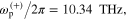
We now turn to the numerical analysis using the full-wave simulation software COMSOL based on the finite element method, for the structure in figure 1(c). Graphene is modeled as a layer of small thickness  and bulk permittivity
 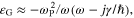 with the quasi-plasma frequency of graphene given by
  The interaction of the electromagnetic wave with the graphene absorber of figure 1(c) is given in figures 6(a)–(e). The absorptance corresponding to metaferrite, dielectric and free space is plotted in figure 6(c); and an excellent agreement with the analytical calculations in figure 4(b) is found, confirming the validity of our analytical equivalent circuit model. The field maps of the electric field norm (figure 6(a)) and the magnetic field norm (figure 6(b)) taken around the frequency of maximum absorptance (i.e. 15 THz) show that the electromagnetic energy is concentrated in the vicinity of the graphene stripes and is of dipolar nature (the stripe acts as an electric dipole in the subwavelength regime:
  The electric and magnetic fields profiles along the dashed lines of figures 5(a)–(d) are also given in figures 6(d)–(f), showing the very high confinement of the fields characteristic of the plasmonic resonance of graphene (energy enhancement
  ).
).
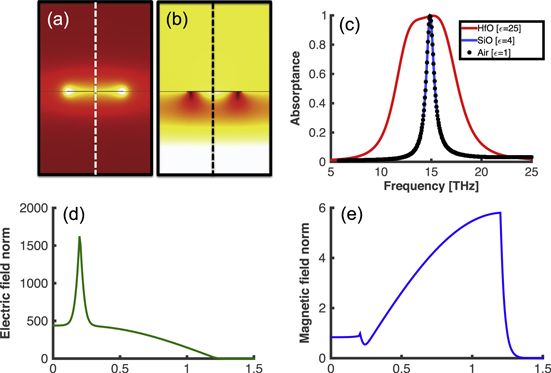
Figure 6. (a) Electric and (b) magnetic field norms profile at the resonance frequency 15 THz. (c) Absorption spectra for the graphene ribbon perfect absorber. (d) Electric and (e) magnetic field plot profiles along the dotted lines in figures 5(a) and (b) respectively.
Download figure:
Standard image High-resolution imageThe concept of metaferrite absorber can also be straightforwardly extended to other frequency ranges. In IR and visible ranges, the kinetic inductance due to the inertia of carrier can be obtained from noble metals (i.e. gold, silver, copper) with a Drude–Sommerfeld complex conductivity. Therefore, a dual inductive–capacitive metascreen at optical frequencies can be accomplished by the lithographic patterning or self-assembly noble-metal nanostructures. At mid-IR and near-IR, some wide-bandgap semiconductors with high electron mobilities and carrier concentrations may be used to make the plasmonic metascreen. Potential candidates for mid-IR plasmonic materials include gallium-doped zinc oxide, aluminum-doped zinc oxide, and indium tin oxide (ITO) [48]. The perfect IR and optical absorbers may be of interest for applications in energy harvesting and spectroscopy.
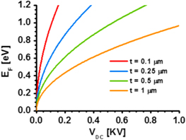
In the final part of this paper, we show the biasing tutorial for an electrically gated graphene sheet. For any variation in the Fermi energy caused by the bias voltage  it is equivalent to the voltage drop
  across the quantum capacitance per unit area
  [49, 50]:

where the quantum capacitance per length  related to the difference between the electron and hole sheet densities (ne and ph (cm−2)), can be expressed as:
and the conventional electrostatic capacitance per unit area is:

where  is the Fermi velocity of graphene,
  is the Boltzmann constant d is the static relative permittivity, and
  is the temperature. Equation (24) must be solved self-consistently to evaluate the relationship between the Fermi energy and the external bias voltages. In general, for relative thick gate oxide (>100 nm),
  is valid, and an explicit expression of Fermi energy for moderately doped graphene, i.e.
  may be derived as:

In some cases,  could be larger than
  due to the finite density of states of graphene. This occurs only when either the value of
  is extremely high or the gate oxide is ultrathin (i.e. few nm). In an extreme case of
  the chemical potential is almost directly responsible for the applied gate voltage, i.e.
  figure 7 reports the dependencies of Fermi energy of graphene on the bias voltage, for various insulating layers. We should note that one drawback of this absorber design resides in the relatively high bias voltage, necessary for achieving the best absorbing performance.
Figure 7. Dependency of Fermi energy versus dc bias for the gated graphene monolayer with different insulator ( thicknesses.
Download figure:
Standard image High-resolution image
Conclusion
We have proposed a tunable multi-band metaferrite, which exploits the dual-reactive properties of the graphene metascreen and the thin metal-backed high- dielectric slab to realize the dual or broadband resonance in the effective permeability in the THz and IR frequency ranges. We have shown that such intriguing magnetic responses may enable the compact, thin THz/IR absorbers with moderately broad bandwidth. We have developed the equivalent circuit model for graphene-based metaferrites and verified the analytical results with full-wave simulations. The graphene metaferrite absorbers show great potential for diverse applications in selective emitters, sensors, spatial light modulators, IR camouflage, THz wireless communication, and thermophotovoltaics.
Acknowledgments
PYC would like to thank the KAUST Winter Enrichment Program (WEP). This work was partially funded by King Abdulaziz City for Science and Technology's TIC (Technology Innovation Center) for Solid-state Lighting at KAUST.