

Abstract
Signal ratiometry plays a crucial role in many measurement fields. Its achievable accuracy is not restricted by the stability of the available signal standard within its linearity limit because the ratio calculations cancel the resultant gain error in the measured signal intensities. However, when there is a significant non-linear response, the multi-point calibration used to reduce the non-linearity error requires one or more stable signal sources. This study describes two progressive methods which reduce the non-linearity error using a ratio-to-phase conversion without a calibrator. We validated our methods' performance using a dc voltage ratiometry experiment.
Export citation and abstract BibTeX RIS

Content from this work may be used under the terms of the Creative Commons Attribution 3.0 licence. Any further distribution of this work must maintain attribution to the author(s) and the title of the work, journal citation and DOI.
1. Introduction
Stable signal sources are used as standards to assess the accuracy of signal measurements but are very challenging to use in practice. For dc voltage measurements, it is sometimes difficult to implement the Josephson voltage standards [1] because they require extremely low temperatures, i.e. the temperature of liquid helium [1] or a little higher temperature [2]. The light source is monitored and controlled by an external light sensor during light intensity measurements, which ensures stability [3, 4]. Although intrinsically stable light sources have recently emerged [5, 6], they have limited wavelength ranges [5] or durability [6]. Consequently, the measured signal intensities typically contain some gain error caused by the instability of the standard.
When the physical quantity of interest (QOI) is calculated using the ratio between the variable measured signal and the nominally constant reference signal, the stability of the standard does not limit the achievable accuracy of the QOI. This is because the ratio cancels the gain error in each signal. In double-beam spectrophotometry [7], the ratio of the sample and reference beam intensities provides sufficient information regarding the linear spectroscopic properties of the sample. Therefore, the measurement accuracy of each intensity does not affect the spectroscopic accuracy. A similar phenomenon occurs for physical measurements based on voltage ratios. For example, temperature measurements using resistance temperature detectors relies on the ratio of both end voltages of a platinum element and a reference resistor in series. Therefore, we do not need accurate measurements of the current going through individual elements, or both end voltages.
However, in these types of measurements, the absence of a stable signal source hinders any further reduction in QOI error because of the non-linearity of the signal measurement. To correct the non-linearity using multi-point calibration, we typically need a stable signal source and multiple signals exhibiting ratios that are sufficiently well calibrated. Manufacturers use accurately calibrated neutral density filters [8] to evaluate the non-linearity of double-beam spectrophotometers at an order of magnitude of  ppm. However, after accurate calibration, there are inevitable time course degradations or filter drifts because of scratches or strains [9]. A similar method was proposed using two polarizers. The relative angles of the polarizers are changed to control the total transmittance. This method has only been applied to reduce large non-linearities of infrared detectors (i.e. which have a resultant error of approximately 1000 ppm) [10]. A practical multi-point calibration depends on a calibrator, which provide multiple outputs that display sufficiently stable, self-calibrating ratios. The double aperture method [11–14] can be used to evaluate non-linearities in double-beam spectrophotometry. In this technique, the apertures of two light signals with a nominal ratio of 0.5 open and close at a constant light source intensity. To calibrate non-linearities over the entire dynamic range, the light source intensity is attenuated in several steps but kept relatively constant. However, this method rarely corrects the non-linearities of actual measurements [15], which is probably because they are difficult to accurately quantify. In voltage ratiometry, manufacturers use resistive voltage dividers [16, 17] as non-linearity calibrators. However, in addition to stability problems, these devices require a time-consuming self-calibration process and highly skilled personnel [18]. The simpler reference step method [19] has achieved an accuracy of less than 0.1 ppm. However, the self-calibration process can be automated if two calibrators output the stability.
The sine-wave histogram test is a method to obtain the non-linearity of A/D converters [20] which exceptionally does not need source stability but does need a pure sine-wave signal source. It is difficult to prepare such sources even for voltage measurement with analog low-pass or band-pass filters [21] and must be impossible without such filters for other measurements such as light intensity. Intermodulation distortion (IMD) relies not on the source stability or spectral purity, but on the linear additivity of the signal. Although a simple formula was proposed to derive the IMD from non-linearity of the transfer function [22], no general methods are known to derive the non-linearity from IMD. Therefore, IMD is rarely used to reduce the non-linearity [23] and is mostly used only as an indicator of the non-linearity.
In this study, we propose a method to reduce the non-linearity error without using stable or linear signal sources like IMD. Although the reduction rate is estimated as a few tens of percent, the method simultaneously reduces the non-linearity error at the measurement without using any calibration data. The reduction rate will be theoretically formulated. Therefore, using the formulation, the original non-linearity can be quantified by scanning the test signal like multi-point calibration. The important advantage of our quantification to the above multi-point calibration is that the correct ratio of the test signal to the reference signal is not required.
2. Basic Concept
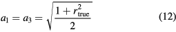
2.1. Ratio-to-phase conversion
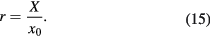
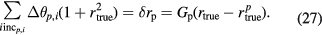
We can convert the ratio of two signals into the phase of a carrier frequency as the following process which we designate as 'ratio-to-phase conversion'. Consider a nominally constant reference signal (x0), the baseline signal or the measurement origin (0), and a variable signal that we want to measure (x1). If these signals are switchable, we can switch them to generate a stepwise periodic signal x(t) (figure 1) with period T. Setting the time origin as the time of the switching from x0 to x1, using Fourier analysis we can derive

where  is the true value of the ratio
  , and θ is the phase of the input signal at the carrier frequency
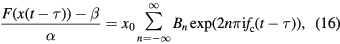
  . Consider a signal detector (SD) that outputs digital data at time t and is described using conversion function F as

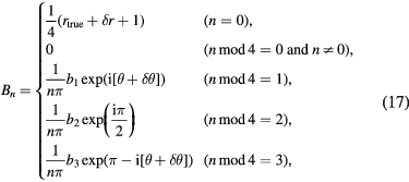
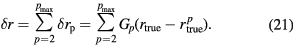
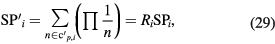
where X(t) is the input, α is the gain, β is the offset, G is the remnant non-linearity function normalized by the gain (see figure 2), τ is the frequency independent time delay of SD (the 'the intrinsic time delay'), and N(t) is random noise (which is negligible for long measurement times). Measuring the stepwise signal with SD provides stepwise output data. The ratio  can be obtained using
  within the linearity limit, by simultaneously implementing a two-point calibration using the step height. That is,

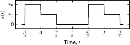
Figure 1. Stepwise time series created by signal switching. The phase of the fundamental frequency is used to determine the ratio  .
.
Download figure:
Standard image High-resolution image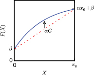
Figure 2. Conversion function of SD. The non-linearity component (defined as G) is schematically emphasized.
Download figure:
Standard image High-resolution imageThe ratio can also be obtained from the Fourier component of the stepwise output using
where  is the phase of the output at
  , which must contain the effect of the intrinsic time delay, τ. In this stage,
  and
and  must both contain the same non-linearity error of G.
2.2. An ideal filter
If an ideal low-pass filter (LPF) or band-pass filter (BPF) with unity gain and no phase shift at a frequency of  is inserted before SD and removes all the harmonics (figure 3), the stepwise signal x(t) is converted into y(t), a sinusoidal signal with or without a dc offset (figure 4). This is defined as

where A is the amplitude, and C is the dc offset. The phase (θ) is equal to that of x(t). Although the signal shape of the output, z(t) in figure 4, is deformed by the non-linearity of SD, z(t) is still an even function at around the peak. Therefore the phase shift is caused only by τ. In this ideal case,  turns out to be equal to
  .
.


Figure 3. Schematic diagram of the basic concept. Stepwise time series, x(t), is filtered and measured. The Fourier transformation unit (FT) outputs the phase of the carrier frequency.
Download figure:
Standard image High-resolution image
Figure 4. Signal shapes of the one-channel system with a LPF. A conversion function as shown in figure 2 is used to exaggerate the signal change by the nonlinearity.
Download figure:
Standard image High-resolution imageAnother variation provides a two-channel sinusoidal output using a two-channel system (figure 5). Without setting a time origin to determine the phase, the difference between the phases of the two output channels gives the true ratio as
where  is the phase difference between the two channels at a frequency of
  , and
, and  is the difference between the intrinsic time delays of the two channels.
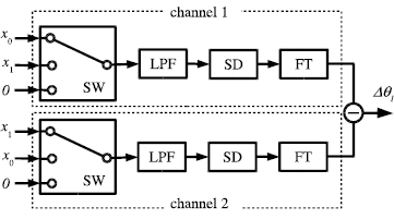
Figure 5. Schematic diagram of the two-channel system with LPF's. The two signal input of channel 1 are exchanged in channel 2. The difference between the phases of the two output channels is used to determine the ratio.
Download figure:
Standard image High-resolution image2.3. Harmonics cancellers
Such an ideal band-pass or low-path filter with no phase shift is generally very difficult to realize. Alternatively, if the signal is additive, the harmonic amplitude of the digital output data can be cancelled using the method described below.
Sinusoidal signal generators for finite harmonics and an adder are inserted before SD (figure 6). The individual sinusoidal signal amplitude and phase are controlled to cancel the harmonics amplitudes generated by the digital output. If all of the harmonics can be cancelled, a sinusoidal output is realized (figure 7) and the SD input signal is

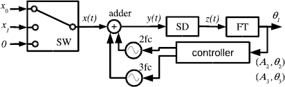
Figure 6. Schematic diagram of the finite harmonics cancellation process. The second and third harmonics are cancelled as an example.
Download figure:
Standard image High-resolution image
Figure 7. Signal shapes obtained using an ideal system with infinite harmonic cancellers. Ratio can be determined as  with no affection of the SD nonlinearity.
Download figure:
Standard image High-resolution imageFor the same reason, the non-linearity of F−1 does not alter the phase at  . Equation (6) still holds, and can be used to determine the ratio that excludes the non-linearity error. The finite harmonics cancellation process is expected to reduce the nonlinearity toward the ideal limit. The extra non-linearity and time delay may be introduced to the system. These factors must be considered to realize an actual system. In the following section, we describe a theoretical approach for evaluating the effect of the finite cancellation.
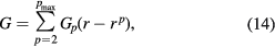
3. Formulation of the harmonics cancellation process
The stepwise signal, x(t), can be expanded as a Fourier series to
where An is the complex amplitude of the n-th harmonic described as
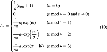


In the above expression, 'mod' is the smallest positive remainder. Equation (11) is equivalent to (1).
We assume that the nonlinearity function, G(X), can be approximated by a finite order power series. That is,
In general, r is a time-series signal with the periodicity of T and composed of multiple order harmonics, and a dc component with zero order harmonic.  in the above expression generates multiple components at the sum frequency of the harmonics composing r.
3.1. Without harmonics cancellation
Consider the case without harmonics cancellation, i.e. when X = x(t). All the n-th order harmonic components generated by non-linearity are added with linear output. The stepwise output signal, F(x(t)), can be expressed as


The components added at  are the origin of the phase shift
  . The phase shift caused by the product of the p components with complex amplitudes (
 ) are
) are


In the above expression, ϕ means the phase difference between the product and the original. If this generated component has the same phase as the original (i.e.  ) it makes no contribution.
For simplicity, let us think about the phase shift at the fundamental frequency. The sum of the harmonic order must be 1. In order to evaluate the phase shift, let us consider the combination of p pieces of integer whose sum is 1. We can classify the combination with respect to the remainders of their harmonic orders devided by 4. For example, if there is only a second order nonlinearity, the phase shift of the fundamental frequency is caused by the combinations

The remainders of all the above combinations are equal to (3, 2), so we classify these combinations into a group. The phase difference from θ is  .
.
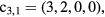
We call these combination groups  , which correspond to nonlinearity order p. i is the numbering of the p-th order combination group. The combination groups for p < 6 are summarized in table 1. Combinations containing 0th order (
 ,
,  etc) are omitted to save space. Combination groups with no phase difference are neglected in table 1. The non-zero phase differences of the products of the corresponding combination groups (
 ) are summarized in table 2.
Table 1. Combination of the remainders by 4, which classify the combinations of harmonic orders causing the phase shift in  .
.
| p | i | combinations of remainders: cp, i | ||
|---|---|---|---|---|
| 2 | 1 | — | — | (3,2) |
| 3 | 2 | — | — | (3,3,3) |
| 4 | 3–5 | (2,1,1,1) | (3,2,2,2) | (3,3,2,1) |
| 5 | 6–8 | (1,1,1,1,1) | (3,3,3,2,2) | (3,3,3,3,1) |
Table 2. Phase differences of each combination.
| i | Phase differences:  |
||
|---|---|---|---|
| 1 | — | — |  |
| 2 | — | — |  |
| 3–5 |  |
 |
 |
| 6–8 |  |
 |
 |
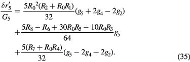
The phase shift of a combination group is


The symbols j0, j1, j2, and j3 denote the number of times 0, 1, 2, and 3 appeared in the remainders, respectively. The symbol  denotes a multinomial coefficient,
  . In the second expression, n denotes the combination of the harmonics order in an element of
  . The term in the summation denotes the product of the reciprocals of non-zero numbers in n. For example,
  can be calculated as
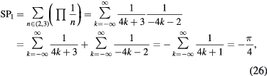
where the Leibniz formula is used in the last line. We can calculate the other  using partial fraction decompositions, as summarized in table 3.
Table 3. Sum of products,  .
.
| i | Sum of products:  |
||
|---|---|---|---|
| 1 | — | — |  |
| 2 | — | — |  |
| 3–5 |  |
 |
 |
| 6–8 |  |
 |
 |
We can verify that
We have confirmed this equation for  using a python library for symbolic calculation (Sympy [24]).
3.2. With the finite harmonics cancellation process
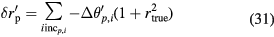
Assume that we can cancel some harmonics,  . Negative order harmonics are inevitablly cancelled together with the positive order harmonics. The input signal to SD is

In this case, the phase shift  can be calculated using equation (24), only if

Here,  is a subset of
  that does not include
  , and Ri for
  is the residual ratio of
  after the cancellation. R0 is the residual ratio of A0 after the cancellation. The nonlinearity error after finite cancellations is
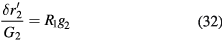
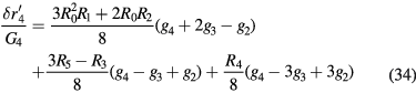
Here, gp is

Note that  is expanded as a linear combination of
  (
( ). Therefore, the nonlinearity function after the cancellation is
The relationship between  and
and  can be expressed using a matrix,
  , that is,
This matrix is called the reduction matrix. It is a function of Ri and is equivalent to the identity matrix when all Ri = 1, without cancellation.
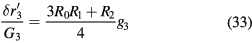
3.3. Cancellation of the second order harmonic : an example
If we cancel the single harmonic, it is straightforward to calculate  . Assume that we have only cancelled the second order harmonic. Then, we can calculate
  using
using

Here,  is a subset of
  whose elements include one or more numbers of
  . For example,
  . Then,
  is −2/3. We calculated the other
  using Sympy [24], which are summarized in table 4. The Ri are given in table 5. The 0-th order residual ratio (R0) obviously equals 1. Assuming
  equals 5, the reduction matrix can be obtained by substituting the Ri results. That is,
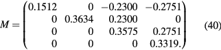
Table 4. Sum of products including the second harmonics,  .
.
| i | Sum of products:  |
||
|---|---|---|---|
| 1 | — | — |  |
| 2 | — | — | 0 |
| 3–5 |  |
 |
 |
| 6–8 | 0 |  |
0 |
Table 5. Residual ratio after the second harmonics cancellation, Ri.
| i | Residual ratio, Ri | ||
|---|---|---|---|
| 1 | — | — |  |
| 2 | — | — | 1 |
| 3–5 |  |
 |
 |
| 6–8 | 1 |  |
1 |
These values are rounded to 4 decimal places.
4. Proposal
We propose two methods to reduce the non-linearity error due to the non-linear component of SD.
4.1. Simultaneous reduction method
As calculated for second harmonic cancellation, the reduction matrix for the cancellation of one harmonic is expected to have the component of the order of 0.1. Therefore only tens of percent of the original nonlinearity will be reduced by one harmonic cancellation. The advantage of this method is simultaneous reduction at the measurement without using any calibration data. For more reduction rate, a multiple cancellation system must be constructed.
4.2. Calibration-like method
If test signal is used for x1 and we scan the measurement range of SD, we can experimentally obtain the change of the non-linearity function,  , by harmonic cancellation. The original non-linearity can be calculated as

where E is identity matrix, '−1' means inverse matrix. This process is like a multi-point calibration, however, the correct ratio is not required for the test signal.
5. Experimental results
A voltage ratiometry experiment was performed to validate the proposed methods. This experiment focused on cancelling the second harmonic using a two-channel, 24-bit, delta-sigma analog-to-digital (A/D) converter (PEX-320724, Interface Corp.) connected to a PC. The non-linearity error and the signal bandwidth of the A/D converter had typical values of 24 ppm and 614.4 kHz, respectively, according to the manufacturers specifications. A block diagram of the experimental instrumentation is shown in figure 8. The signal generator (SG) consisted of three 1.3 V Ni-MH rechargeable batteries (Eneloop, Sanyo) and a six-resistor voltage divider. The signal output (V0 or x0) was nominally fixed at 3.9 V, and the signal V1 (or x1) could be switched from 0 to 3.9 V in six approximately equal steps. To estimate the non-linearity errors in  and
and  , we measured the ratio of the generated signals (
 ) using the ratiometer function of a digital voltmeter (6581, ADCMT). We regarded this value as
  , and used it to calculate the nonlinearity errors. According to its specifications, the voltmeter was 1 μV accurate, which is equivalent to approximately 0.3 ppm ratiometry error. The system was designed to provide a carrier frequency (
 ) of 307.2 Hz. A 12.288 MHz square wave produced by a function generator FG1 (WF1947, NF Corp.) was input into a field-programmable gate array (FPGA) board (DE0, Terasic) as a base clock (clk0). This clock was divided by 80 000 to generate two
  square signals with a 90 degree phase difference (clk1 and clk2), or by 40 000 to form a
  square signal (clk3). These signals were used as clocks to drive analog switches in a switching board (SB). The base clock (clk0) was also divided by 20 to give a 614.4 kHz sampling clock (clk4), which was common to both channels of the A/D converter.

Figure 8. Block diagram of the system. FG1 is the function generator that supplies a base clock (clk0) to FPGA; FG2 is the function generator that supplies the second harmonic signals (S1 and S2) to SB; SG is the signal generator that outputs two dc voltages (V0 and V1); FPGA represents the FPGA board supplying clocks (clk1, ..., 4), which drive the analog switches, DVM is the digital voltmeter; SB is a switching board; and A/D is a 2-channel AD converter.
Download figure:
Standard image High-resolution imageFigure 9 shows that the input signals of the switching board from SG alternated with each other and with the ground level signal using four analog switches ( ; MAX4527 [25], Maxim). The behavior of theses switches is described in figure 10. The timing chart of the three clocks is also shown in figure 11. The stepwise signals were input into two voltage adders composed of inverting amplifiers installed at the pre-stages of the A/D convertor input channels. The second harmonic cancellation was performed by adding two sinusoidal waves (H1, H2) of 614.4 Hz, produced by a two-channel 16-bit function generator FG2 (WF1948, NF Corp.).

Figure 9. Circuit diagram of the switching board.  are analog switches that can exchange two-channel inputs, as described in figure 10. 10 k and 100 k are 10 k
  and 100 k
  resistors. The two components enclosed in red rectangles work as voltage adders.
Download figure:
Standard image High-resolution image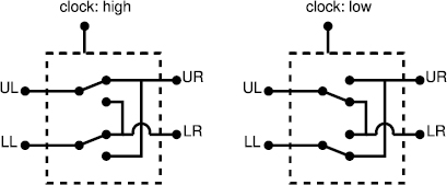
Figure 10. Behavior of analog switches. When the clock input (clk) is high, the upper left terminal (UL) is connected to the upper right terminal (UR), and the lower left terminal (LL) is connected to the lower right terminal (LR). When clk is low, UL is connected to LR and LL is connected to UR.
Download figure:
Standard image High-resolution image
Figure 11. Stepwise signal shape obtained from each channel without the harmonic cancellation. The voltage ratio  was calculated from the mean values, (
 ,
,  , and
, and  ) of the data at the corresponding time segments (non-colored areas), i.e.
  ,
,  and
and  , as in equation (9). The timing charts of the three clocks are shown at the bottom.
Download figure:
Standard image High-resolution imageBefore the measurement, both input terminals were connected to the ground level to get baseline signals of both channels, including the operational amplifier offset and the switching noise. These baseline signals were digitally subtracted from all the measured signals to cancel this offset and noise. The second harmonic amplitude of each channel displayed on the PC was reduced to less than 0.1% by manually controlling the phase and amplitude of each FG2 channel. The digital output data from A/D were stacked in 2.5 s intervals, and averaged into a 4000-long array corresponding to one cycle of clk1 and clk2 (=2 T), to suppress any random noise. A dead time of 1.5 s is set after each stacking time, to calculate the phase and save it to a hard drive. The voltage signal time series is not saved, to reduce dead time. However, figures 11 and 12 show examples of this signal before and after the harmonic cancelling, where V1 is half V0. To eliminate the effects of switching noise and transition times, the stepwise digital data without harmonic cancellation was separately added in time segments 
 and
and  (figure 11) to calculate the averages
  ,
,  and
and  . The ratio
  was calculated using
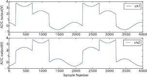
Figure 12. Signal shape with second harmonic cancellation. This is an example data when V1 is set to about the half of V0.
Download figure:
Standard image High-resolution image6. Results and discussion
Figure 13 shows the rough behavior of the obtained data. The pink colored bands represent time ranges when the harmonics were not canceled, and the blue bands are time intervals where they were canceled. The other time ranges are periods when FG2 was manually set. The values of  plotted in (a) correspond to
  in equation (7). All three kinds of ratio (
 ,
,  and
and  ) are plotted in (b) at the plotting resolution. The black dots in (c) represent the time variance of the nonlinearity error determined from the difference between
  and
and  , which is typically called the integral nonlinearity (INL) in the voltage measurement. The red dots in (c) represent the INL for
  .
.  was determined in such a manner that the INL was 0 when the ratio was 1. A reduction in INL is clearly seen in the range of the ratio between 0.5 and 0.8.

Figure 13. Time series variation of averaged data acquired every 4 seconds. The pink colored bands represent time ranges when the harmonics were not canceled, and the blue bands are time intervals where they were canceled. The other time ranges are periods when FG2 was manually set.
Download figure:
Standard image High-resolution imageIn order to evaluate 'simultaneous reduction method' more precisely, the mean value and standard error of the INL data were calculated for each time range and plotted in figure 14. As estimated in the proposal, reduction rate is only a few tens of percent. For more reduction, we have to increase the cancellers for higher order harmonic cancellation. Before canceling, the INL of  is coincident with the INL of
  , within a 1 ppm precision. The differences are significantly larger than the standard error of the data, and larger than the error of
  (0.3 ppm in the DVM's specification). One possible cause is the drift of
  . Such a small drift may be concealed behind the scattered data in figure 13. Precise measurement of the ambient temperature may prove the drift if such differences correlate to the temperature change. Electronic devices used in the switching board may have some nonlinearities. However, these would have a similar influence on both
  and
and  , and cannot be the cause of the difference.
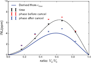
Figure 14. INL before ( : red marks;
  : black marks) and after (
 : blue marks) harmonic cancelling. The black line is the fitting curve of the fifth order function to
  . The blue line is the theoretically derived nonlinearity after cancelling the second order harmonics from the black line using the reduction matrix.
Download figure:
Standard image High-resolution imageThe unknown nonlinearity of the switching board is the previous stage of the adders and should not be reduced by the harmonic cancellation. However, we ignored this nonlinearlity and analyzed the data regarding the INL of  as the nonlinearity of the SD to be reduced. The black line in figure 14 is a quintic curve determined by a least square fit to the INL. The blue line is the nonlinear function derived from the black curve and the reduction matrix. This line agrees with the nonlinearity of
  (blue dots) within approximately a 1 ppm precision. This difference is on the same level as that between
  and
and  before cancellation, and can also be interpreted as the result of the drift of
  . The nonlinearity of the switching board is presumed to be small compared to the observed INL, because no contradictions are found if we ignore it.
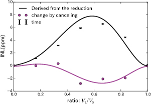
Using the reduction matrix, the INL of SD must be estimated from the phase alteration due to the harmonic cancellation which has been proposed as 'calibration-like method'. The purple dots in figure 15 represent the difference of INL calculated from the phase change due to the second harmonic cancellation without using the correct ratio ( ), from the DVM. The purple line in the figure is a quintic curve determined by a least squares fit. The black line is the INL estimated by multiplying the coefficient vector by the inverse matrix of E − M, which agrees with the INL of
  within a 1 ppm precision. The drift of
  is also a possible cause of this difference. The nonlinearity of the switching board is also included in this difference, and is therefore not larger than approximately 1 ppm.
Figure 15. INL estimation from the reduction by cancelling. We did not use data from the digital voltmeter.
Download figure:
Standard image High-resolution image
7. Conclusion
We proposed ratio-to-phase conversion to reduce the non-linearity error for obtaining the ratio of a variable signal to a nominally constant reference signal. Finite harmonic cancellation simultaneously reduces the nonlinearity errors due to the signal detector, which was proposed as 'simultaneous reduction method'. The reduction matrix can be used to estimate the nonlinearity of the signal detector from the partial reduction after the finite harmonic cancellation which was proposed as 'calibration-like method'. The effects of the two methods were verified with a second harmonic cancellation experiment. These methods will also be useful for detecting other signals that have additivity such as optical intensities with reduced nonlinearity errors. Furthermore, this method can be extensively applied to detect small nonlinearity components of response systems with such additive signals.
Acknowledgment
This study was supported by a Japan Society for the Promotion of Science Grant-in-Aid for Challenging Exploratory Research (No. 24656062). The author has a competing interest with an international patent application No. PCT/JP2015/069026 relative to this study. The authors would like to thank Enago (www.enago.jp) for the English language review.