

Abstract
In order to understand the optoelectronic properties of amorphous niobium oxide (a-NbOx), we have investigated the valence states, local structures, electrical resistivity, and optical absorption of a-NbOx thin films with various oxygen contents. It was found that the valence states of Nb ion in a-NbOx films can be controlled from 5+ to 4+ by reducing oxygen pressure during film deposition at room temperature, together with changing the oxide-ion arrangement around Nb ion from Nb2O5-like to NbO2-like local structure. As a result, a four orders of magnitude reduction in the electrical resistivity of a-NbOx films was observed with decreasing oxygen content, due to the carrier generation caused by the appearance and increase of an oxygen-vacancy-related subgap state working as an electron donor. The tunable optoelectronic properties of a-NbOx films by valence-state-control with oxygen-vacancy formation will be useful for potential flexible optoelectronic device applications.
Export citation and abstract BibTeX RIS
1. Introduction
Niobium oxide (NbOx) is one of the transition metal oxides, which exhibit a rich variety of optoelectronic properties due to the flexible multi-valent nature of transition metal ions [1, 2]. NbOx has been classically known to exist as three stable phases of  (4d 0), Nb4+O2 (4d1), and Nb2+O (4d3) with distinct valence states of Nb ion [3]. Nb2O5, the most thermodynamically stable phase, is a transparent insulator with a bandgap of ~3.7 eV [4] and has wide-ranging applications, such as solid-state capacitors [5] and optical coatings [6]. NbO2 shows a reversible metal–insulator (MI) transition at a high temperature of 1083 K [7]; the MI transition occurs in association with structural distortion, which consequently induces electronic-structure reconstruction to open up a charge gap of ~1.6 eV [8]. The MI transition in NbO2 is useful for electrical switching applications, operating potentially at high temperature [9]. The most reduced phase NbO is a good metallic conductor [10], and moreover it shows superconductivity at 1.5 K [11]. Since the valence state of Nb ion is quite variably dependent on the oxide-ion (O2−) off-stoichiometry and the coordination states, the optoelectronic properties can be tuned dramatically from insulator to metal by valence-state-control with oxygen-vacancy formation in the NbOx phases.
In addition to the various features observed for crystalline phases, NbOx can be formed as an amorphous (a-) film at room temperature (RT) when the film is deposited without heating [12, 13], which is attractive for flexible device applications. Considering the giant physical response to the valence states in the NbOx phase, a-NbOx film appears interesting for optoelectronic switching devices by controlling the phases between a-NbOx with different valence states. Actually, good characteristics have been obtained in a resistive random access memory (ReRAM) [14] and an electrochromic device [15, 16]. However, there have been few studies on optoelectronic properties of a-NbOx films with controlled valence states; to our knowledge, a-NbOx films with different x have not been reported up to now. It is highly desirable to clarify their optoelectronic transport properties by introducing the O2− off-stoichiometry in a-NbOx films, because the O2− ion arrangement around Nb ion in a-NbOx films with different valence states should dramatically affect their properties.
In this paper, we report the optoelectronic properties of a-NbOx thin films with controlled valence states of Nb ion. Here we fabricated a-NbOx films by pulsed laser deposition (PLD) at RT, where the oxygen pressure ( ) during film growth was controlled to largely change the oxygen content (x) in a-NbOx film. It was found that the valence state of Nb ion can be controlled from 5+ to 4+ by changing
  , where the coordination environment of Nb ions was changed from Nb2O5-like to NbO2-like local structure. As a result, the electrical resistivity of a-NbOx films was modulated to a large extent, due to the carrier generation caused by the appearance and increase of the oxygen-vacancy-related subgap state working as an electron donor. These results provide useful information on the application of a-NbOx films for flexible optoelectronic devices.
2. Experiment
The a-NbOx films were fabricated on alkali-free glass substrates (Corning® EAGLE XG®) under  = 1.5 × 100 − 1.0 × 10⁻³ Pa by PLD at RT. A KrF excimer laser (wavelength of 248 nm) was used to ablate a Nb2O5 polycrystalline target disk, where the laser energy fluence and repetition rate were ~2 J cm−2 pulse−1 and 10 Hz, respectively. Figure 1 shows a high-angle annular dark-field scanning transmission electron microscopy (HAADF-STEM) image of the a-NbOx film fabiricated under
  of 1.0 Pa. An STEM image of an a-NbOx film region was observed with bright contrast due to heavier Nb ions and supports the highly homogeneous and continuous film structure. The inset shows a selected area electron diffraction pattern, observed by TEM, for the a-NbOx film; a broad halo feature was seen, confirming the amorphous structure. The amorphous nature of all the other films was also confirmed by grazing incidence x-ray diffraction (incident angle ω was fixed at 0.3°); no crystalline phase was observed. We have evaluated the valence states, local structures, electrical resistivity, and optical absorption of these a-NbOx films fabricated under different
  .
.

Figure 1. Cross-sectional high-angle annular dark-field scanning transmission electron microscopy (HAADF-STEM) image of amorphous niobium oxide (a-NbOx) film fabricated on a glass substrate at room temperature under oxygen pressure ( ) of 1.0 × 100 Pa. The inset shows a selected area electron diffraction pattern for the a-NbOx film region, recorded by TEM.
Download figure:
Standard image High-resolution image3. Results
3.1. Valence state and local structure analysis
We first investigated the valence states and local structures of a-NbOx films with respect to the change of  , by Nb K-edge x-ray absorption fine structure (XAFS) measurements on 200 nm thick a-NbOx films. The XAFS measurements were performed with a fluorescence mode at the NW10A beamline of the Photon Factory in the High Energy Accelerator Research Organization (KEK-PF), Japan6, where the energy resolution of the beamline is estimated as ca. 4 eV at 19 keV. Figure 2(a) shows normalized x-ray absorption near-edge structure (XANES) spectra; the Nb K-edge feature clearly changed depending on
  . The
. The  dependence of the edge energy (E0), which was defined as the energy giving the half value of the normalized continuum absorption in arbitrary units, is summarized in the inset of figure 2(a). E0 clearly shifted to lower energy with decreasing
  , indicating the reduction of the valence state of Nb ion [17]. We also observed the valence-state change of Nb ion by x-ray photoemission spectroscopy (XPS, figure 3). For a-NbOx films fabricated under
  = 1.5 Pa, only the Nb5+ 3d peak was observed in the core level spectra, whereas, for a-NbOx films fabricated under lower
  , the Nb4+ 3d peak appeared along with the Nb5+ one, and the peak intensity ratio of Nb4+/Nb5+ increased with decreasing
  , supporting the hypothesis that the electronic configuration of Nb ion changed from [Kr]4d 0 (Nb5+) to [Kr]4d1 (Nb4+) by decrease of
  . Figure 2(b) shows k3-weighted extended XAFS (EXAFS) oscillations of the a-NbOx films, along with those of polycrystalline Nb2O5 and NbO2 for comparison. The EXAFS oscillation shape of a-NbOx films systematically changed from a Nb2O5-like pattern to NbO2-like pattern by decreasing
  ; in the high wave vector region (k ⩾ 6), the peak separation, which is a characteristic change from a NbO2-like to Nb2O5-like pattern, was observed in a-NbOx films with increasing
  . Figure 2(c) summarizes the Fourier-transformed (FT) magnitudes of the k3-weighted EXAFS oscillations as a function of the phase-uncorrected interatomic distance (R). The FT magnitudes at R ⩾ 2.5 Å were significantly suppressed, and only the first shells for the Nb–O bonding survived due to the amorphous structure. The R of Nb−O bonding increased and got closer from that of polycrystalline Nb2O5 to NbO2 with decreasing
  (the inset of figure 2(c)), suggesting the transformation of the O2− coordination state around Nb ion from Nb2O5-like to NbO2-like structure. The a-NbOx films with Nb–O polyhedra seem comparable to the glass state as in silicate glasses with building block SiO4; the a-NbOx films with a short range order of building units can be considered as a non-crystalline material, although they have no long range order (amorphous phase). These features can also be seen in the XANES spectra (figure 2(a)), where the pre-edge shoulder, as indicated by a black arrow, was observed for a-NbOx films fabricated at high
  . To clearly show the change, the normalized pre-edge spectra for a-NbOx films and those for polycrystalline Nb2O5 and NbO2 are compared in supplementary figure S16. The pre-edge shoulder has been reported to depend on the coordination state of niobium compounds [18]; it was observed for Nb2O5, but was not observed for NbO2 crystals. The normalized pre-edge peak was clearly observed for the a-NbOx films fabricated at high
  of 1.5 and 0.7 Pa, but it abruptly disappeared in the films fabricated at lower
  , further supporting the hypothesis that a-NbOx films changed from Nb2O5-like to NbO2-like local structure. These results indicate that the valence state of Nb ion can be controlled from 5+ to 4+ by changing
  , along with the change of the coordination environment of Nb ions from Nb2O5-like to NbO2-like local structure. It should be noted that, according to the equilibrium phase diagram of crystalline NbOx with respect to oxygen pressure [19], the Nb2O5 phase is stable in a wide range, while NbO2 is obtained only in highly reduced conduction at RT; the control of x in NbOx is difficult in the equilibrium state. The present a-NbOx films fabricated by PLD are considered to be in the non-equilibrium state and the x can be easily controlled by
  during vapor phase deposition, where the kinetic effect on the mass transport in vapor is dominant.
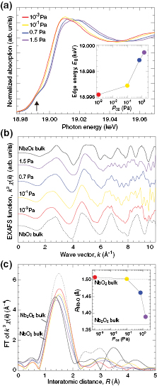
Figure 2. Valence state and local structure analyses of a-NbOx films fabricated under  from 1.5 × 100 to 1.0 × 10⁻³ Pa. (a) Normalized Nb K-edge XANES spectra. The black arrow indicates the position of the pre-edge shoulder. The absorption edge energy (E0), determined at the middle point of normalized absorption intensity, is summarized in the inset. E0 shifts to lower energy with decreasing
  , indicating the reduction of the Nb valence state. (b) k3-weighted EXAFS oscillations of the a-NbOx films, along with those of Nb2O5 and NbO2 polycrystalline for comparison. (c) FT magnitudes of the k3-weighted EXAFS oscillations, as a function of the phase-uncorrected interatomic distance (R). The inset summarizes the
  dependence of R for Nb–O bonding. The O2− coordination state in a-NbOx films changes from Nb2O5-like to NbO2-like local structure with decreasing
  .
.
Download figure:
Standard image High-resolution image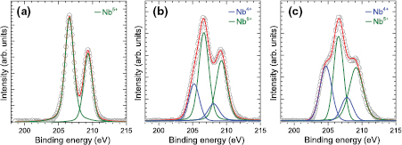
Figure 3. Nb 3d XPS spectra with monochromated Al Kα (hν = 1486 eV), measured for the a-NbOx films fabricated under different  of (a) 1.5 × 100, (b) 3.0 × 10⁻¹, and (c) 1.0 × 10⁻³ Pa. The binding energy was calibrated with reference C 1s peak (285.0 eV). After background subtraction, the Nb 3d core level spectra can be resolved into two pairs of peaks, where each pair corresponds to the spin–orbit-splitting of 3d5/2 and 3d3/2 levels. Green and blue lines are fitting curves for two different Nb valence states of 5+ and 4+ , respectively.
Download figure:
Standard image High-resolution image3.2. Carrier transport properties
Then we measured temperature dependence of electrical resistivity (ρ–T) for the valence-state-controlled a-NbOx films, by the dc four-point probe method with van der Pauw configuration (the film thickness was fixed at 100 nm). Figure 4(a) shows ρ–T curves for the a-NbOx films in the T range of 300–20 K. Although the a-NbOx film at  = 1.5 Pa was highly insulating (ρ was not in the measureable range), ρ at RT was largely reduced from 9.2 × 101 Ω cm to 2.8 × 10⁻² Ω cm by changing
  from 1.0 × 100 to 1.0 × 10⁻³ Pa. For the temperature dependence of resistivity, an exponential increase of ρ with respect to the temperature, i.e. semiconducting behavior, was observed for all the a-NbOx films throughout the whole temperature range. Arrhenius plots (log σ − 1000/T) are summarized in figure 4(b); log σ does not follow a simple thermally activated behavior. At T > 200 K, a linear slope is observed, indicating the band conduction of thermally activated charge carriers. In contrast, at T < 200 K, the Arrhenius plots exhibit large deviations from straight lines, where log σ transforms to much weaker temperature dependence. Better straight lines are obtained in the log σ versus T −1/4 plots (figure 4(c)) at a low temperature of 150–20 K: log σ can be fitted well by two distinct T −1/4 scaling behaviours, indicating variable range hopping (VRH) conduction in the low temperature regime [20]. These results clearly support the hypothesis that the carrier transport in a-NbOx films is largely modulated by valence-state control with oxygen-vacancy formation.

Figure 4. Electrical properties of a-NbOx films as a function of  from 1.0 × 100 to 1.0 × 10⁻³ Pa. (a) ρ–T curves. All the films showed semiconducting behavior, but ρ was largely modulated by changing
  . (b) Log σ versus 1000/T plots. The solid line indicates the linear slope in log σ at T = 300 − 200 K, but a severe deviation was observed at lower temperature. (c) Log σ versus T −1/4 plots at a low temperature of 150 − 20 K. Log σ can be fitted well by two distinct T −1/4 scaling behaviors.
Download figure:
Standard image High-resolution image3.3. Optical properties
Since the carrier transport in the a-NbOx films should be closely related to the localized defective states, optical absorption spectra were measured by UV-vis/NIR microscopy at RT. Figure 5 shows the absorption coefficient (α) in the energy range up to 6.0 eV. A fundametal absorption edge was clearly observed for a-NbOx film at high  = 1.5 Pa, whereas an additional absorption band appeared just below the absorption edge and became larger with decreasing
  . The inset summarizes the
  dependence of the optical bandgap, estimated by Tauc plots of the a-NbOx films (supplementary figure S26). For a-NbOx films at high
  = 1.5 Pa, the Tauc gap (Eg) was estimated to be 3.8 eV, which is almost the same as previously reported values of ~3.4 eV for the a-Nb2O5 phase [21], ~3.7 eV for the Nb2O5 crystalline phase [22, 23]. With decreasing
  , Eg significantly decreased and saturated at ~1.6 eV, due to the appearance of the subgap state. These results suggest that the optical bandgap of a-NbOx films basically originates from the electronic structure of the a-Nb2O5 phase and the oxygen-vacancy-related subgap state is formed by decreasing
  .
.

Figure 5. Absorption coefficient (α) of a-NbOx films as a function of  from 1.5 × 100 to 1.0 × 10⁻³ Pa. The arrow indicates the peak position of the additional absorption band. The inset summarizes the optical gap (Eg), estimated from Tauc plots. For a-NbOx films fabricated under
  = 1.5 × 100 Pa, Eg was estimated to be ~3.8 eV, whereas for the films fabricated at lower
  , Eg decreased down to ~1.6 eV because of the appearance and increase of the subgap state with decreasing
  .
.
Download figure:
Standard image High-resolution image3.4. Thermopower analysis
Figure 6 summarizes the correlation between σ at RT and αs (α at peak position ~3.1 eV of the subgap state), together with thermopower (S). S is a powerful measure to evaluate the relationship between electronic structure and carrier transport, because S basically reflects the energy differential of the density of states (DOS) at the Fermi energy [24, 25]. The inset shows thermoelectromotive force (ΔV) versus temperature gradient (ΔT) for the a-NbOx films, where the actual temperatures at both sides of the film surface were monitored by two tiny thermocouples. S was obtained from the linear slope of the ΔV–ΔT plots; S values were always negative, indicating n-type conduction of the a-NbOx films.

Figure 6. The relationship between σ and αs (α at peak position ~3.1 eV of the subgap state), together with thermopower (S) at RT. (a) σ versus αs plots. σ increases with increasing αs, suggesting that σ is affected to a large extent by the appearance and increase of the subgap state. (b) σ versus S plots. S was obtained from the linear slope of each ΔV–ΔT plot (inset). S values were always negative, indicating n-type conduction of a-NbOx films. The S–log σ plot shows the linear decrease with the gradient of −kB/e · ln 10 (=−198 μV K−1 decade−1), indicating that the σ modulation originates from the change of carrier concentration in the a-NbOx films.
Download figure:
Standard image High-resolution imageBoth S and αs are closely correlated with σ. αs increased with increase of σ, suggesting that σ was affected by a large amount by the appearance and increase of the subgap state. In addition, |S| monotonically decreased from 721 μV K−1 to 77 μV K−1 with an increase of σ; the gradient of the linear slope in S–log σ is −182 μV K−1 decade−1. In general, semiconductors possessing a parabolic DOS show a linear relationship between |S| and the log of carrier concentration (ne): |S| = −kB/e·ln 10 (log ne + C), where C is parameter that depends on the type of materials [26]. When considering that the electron mobility is constant for all a-NbOx films7, the observed linear slope corresponds well with −kB/e·ln 10 (=−198 μV K−1 decade−1), suggesting that electrons are doped into the conduction band, and the gradient of DOS becomes moderate, similar to carrier doping in conventional semiconductors. It should be noted that only Nb d-band conduction is considered here, but other conduction mechanisms, such as narrow band conduction thourgh localized hopping and tunneling processes, may contribute to conduction in a-NbOx films. However, the linear relation between |S| and log σ suggests that Nb d-band conduction should be dominant at RT. These results suggest that the increase of σ with respect to  originates from the change of carrier concentration in the a-NbOx films due the appearance and formation of the oxygen-vacancy-related subgap state working as an electron donor.
4. Discussion
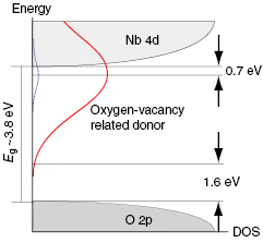
We summarize the present results by constructing the electronic structure model (figure 7). At  = 1.5 Pa (a-NbOx film is in the highly insulating state), the conduction band is composed of unoccupied Nb 4d 0 orbital, which is the electronic structure of a-Nb2O5 with Eg = 3.8 eV. With decreasing
  , oxygen-vacancy formation in a-NbOx films changes the O2− arrangement around Nb ion from Nb2O5-like to NbO2-like local structure, along with the Nb valence-state change from 5+ to 4+. As a result, the subgap state appears as an electron donor at below the conduction band bottom and the DOS increases due to the increase of oxygen off-stoichiometry in a-NbOx films; consequently, Eg is reduced down to 1.6 eV, which is the primary origin of the large electrical resistivity modulation in the present a-NbOx films.
Figure 7. Schematic illustration of the electronic structure for a-NbOx films. For high  = 1.5 × 100 Pa, the conduction band is composed of unoccupied Nb 4d 0 orbital, which is the electronic structure of Nb2O5 with Eg = 3.8 eV. With decreasing
  , the subgap state appears as an electron donor at below the conduction band bottom and the DOS increases due to the increase of O2− off-stoichiometry in a-NbOx films; consequently, Eg is reduced down to 1.6 eV.
Download figure:
Standard image High-resolution image
5. Conclusions
We have investigated optoelectronic properties of valence-state-controlled a-NbOx thin films. It was found that the valence states of Nb ion in a-NbOx films can be controlled from 5+ to 4+ by changing  during film growth by PLD at RT, where the coordination environment of Nb ions was changed from Nb2O5-like to NbO2-like local structure. As a result, a four orders of magnitude modulation of electrical resistivity for a-NbOx films was observed, due to the carrier generation caused by the appearance and increase of the oxygen-vacancy-related subgap state working as an electron donor. The tunable optoelectronic properties of a-NbOx films by valence-state-control with oxygen-vacancy formation will offer potential applications in flexible optoelectronic devices.
Acknowledgments
The authors would like to thank Profs H Hosono, H Hiramatsu, and K Ide for optical measurements, and N Kawai for experimental help on TEM/STEM analyses. The optical measurements were supported by the Collaborative Research Project of the Materials and Structures Laboratory, Tokyo Institute of Technology. The TEM/STEM analyses, conducted at Hokkaido University, were supported by the Nanotechnology Platform Program from MEXT. The Nb–K edge XAFS experiments were performed under the approval of the Photon Factory Program Advisory Committee (Proposal No. 2014G547). This work was supported by Grant-in-Aid for Scientific Research on Innovative Areas (25106007), Grant-in-Aid for Scientific Research A (25246023) from JSPS and the Network Joint Research Center for Materials and Devices. TK was supported by Grant-in-Aid for Young Scientists A (15H05543) and Grant-in-Aid for Challenging Exploratory Research (16K14377) from JSPS.
Footnotes
- 6
See supplementary material (stacks.iop.org/JPhysCM/28/255001/mmedia) for XAFS measurements and optical analyses.
- 7
We performed ac and dc Hall effect measurements at RT to estimate the carrier concentration of a-NbOx films, but reliable Hall voltages were not obtained, due to the low carrier mobility (⩽0.1 cm2 V−1 s−1), presumably reflecting Nb 3d-band conduction.