

Abstract
Over the past decade magnetoelectric (ME) mutiferroic (MF) materials and their devices are one of the highest priority research topics that has been investigated by the scientific ferroics community to develop the next generation of novel multifunctional materials. These systems show the simultaneous existence of two or more ferroic orders, and cross-coupling between them, such as magnetic spin, polarisation, ferroelastic ordering, and ferrotoroidicity. Based on the type of ordering and coupling, they have drawn increasing interest for a variety of device applications, such as magnetic field sensors, nonvolatile memory elements, ferroelectric photovoltaics, nano-electronics etc. Since single-phase materials exist rarely in nature with strong cross-coupling properties, intensive research activity is being pursued towards the discovery of new single-phase multiferroic materials and the design of new engineered materials with strong magneto-electric (ME) coupling. This review article summarises the development of different kinds of multiferroic material: single-phase and composite ceramic, laminated composite and nanostructured thin films. Thin-film nanostructures have higher magnitude direct ME coupling values and clear evidence of indirect ME coupling compared with bulk materials. Promising ME coupling coefficients have been reported in laminated composite materials in which the signal to noise ratio is good for device fabrication. We describe the possible applications of these materials.
Export citation and abstract BibTeX RIS
Introduction
Ferroelectric (FE) and ferromagnetic (FM) materials have been widely studied and have led to important scientific and technological advances. Different origins of ferroelectricity have been explored, such as charge ordering, magnetically induced ferroelectricity, lone-pair electron effects, octahedral distortion, strain mediation, geometrical frustration etc, but in general, ferroelectricity results from relative shifts of negative and positive ions that induce surface charges; usually it requires formally empty d orbitals, but on the other hand, magnetism is related to the ordering of spins of electrons in incomplete ionic shells, that is, it results from partially filled d orbitals. Ferroelectric materials are used to make capacitors with a high dielectric constant, transducers and actuators, which are not switching devices; and their memory applications exploit their hysteresis properties, which results in two stable states of opposite polarisation. Similarly, ferromagnetic materials are used in many industrial applications, such as sensors, read heads and memories based on giant magnetoresistive effects, for which they are already commercially available [1]. Another novel class of multifunctional materials, known as magnetoelectric (ME) multiferroics (MF) possess simultaneously ferroelectric and ferromagnetic properties in the same phase and exhibit linear coupling; they have received much research interest due to both the basic physics and the number of potential multi-functional applications, such as nonvolatile memory elements, magnetic field sensors and actuators, nano-electronics, energy harvesters, ferroelectric photovoltaics etc. These multifunctional materials are quite interesting and generate strong ME coefficients from cross coupling among various ferroic order parameters; in ME systems, magnetic spins can be switched by an external electric field and spontaneous polarisation by external magnetic fields. Multiferroics are likely to offer additional functional parameters including more than two logic states for a whole range of new applications [2]. These ME materials often combine the potential properties of their parent FE and FM materials; in addition they have bifunctional properties not available in systems with a single order parameter. The search for these materials is driven by the prospect of controlling charges by applied magnetic fields and spins by applied voltages and using this to construct new forms of multifunctional devices [3, 4]. The coexistence of magnetisation and electric polarisation might allow an additional degree of freedom in the design of novel devices such as actuators, transducers and storage devices. Other potential applications include multiple-state memory elements, in which data is stored both in the electric and the magnetic spins, or novel memory media that might allow the writing of the ferroelectric polarisation data bit with an electric field and reading the data bit with associated magnetic fields [5]. These properties are very useful in the development of low power nanoelectronics memory elements.
Single-phase multiferroic materials have been reported in small numbers due to the contra-indication mentioned above between the conventional mechanism in ferroelectric oxides that requires empty d-orbitals and the formation of magnetic moments, which results from partially filled d-orbitals [1, 6, 7]. Alternatively, the fabrication of artificial multiferroics includes the possibility of tailoring the properties using two different compounds, one being ferromagnetic and other ferroelectric. The aim of this technique is to create materials that display properties of the parent compounds and their coupling. These composite multiferroic ceramics have been found to exhibit a larger ME effect than that of the single-phase materials by more than one order of magnitude [8]. However, the advances in thin-film growth techniques have provided routes to structures and phases that are inaccessible by chemical methods, generating attention towards composite ME materials, especially thin films. Nano-structuring is a promising approach that has opened the door to the design of practical devices based on ME coupling. Thin-film multiferroics is beginning to reveal a range of fascinating phenomena as well as to stimulate the exploration of new device heterostructures, which have potential applications in microdevices and integrated units such as microsensors, micro-electro-mechanical systems (MEMS) devices and high-density information storage. Much effort has been made to synthesise ME heterostructure thin films where FE and FM properties coexist for the next generation miniaturised integrated devices. Several configurations have been employed to fabricate ME composite thin films: composites with FE or FM terminal layers, multilayer nanostructures, superlattice structures with alternate FM and FE layers and epitaxial ferroelectromagnetic nanocomposites fabricated by self-assembly technique. These nanostructured thin films have shown significant ME coupling coefficients with great potential for future ME devices [9].
Each stage of the development of multiferroic materials will be presented in more detail in the subsequent sections of this article along with some examples of newly developed materials in each class of multiferroic that has been investigated and recently published. The last part of the review article will be devoted to the possible applications of magnetoelectric multiferroic materials.
Background and history of multiferroics and magnetoelectrics
Bulk single phase multiferroics
Two independent events marked the birth of the ME: (i) In 1888 Röntgen discovered that a moving dielectric became magnetised when placed in an electric field [10]; the opposite effect was observed 17 years later (the polarisation of a moving dielectric in a magnetic field) [11]. (ii) In 1894 Curie pointed out the possibility of the intrinsic ME behaviour of crystals on the basis of symmetry considerations, in which the crystals can be polarised in the presence of a magnetic field, and vice-versa. Later, Dzyaloshinskii provided theoretical details of the ME in a specific material—Cr2O3 [12]; subsequently, in 1960, Astrov reported the first experimental observation of the ME effect in Cr2O3, and he showed experimental confirmation of an electric field induced magnetisation [13, 14], and Rado et al [15, 16] quickly confirmed the converse magnetic field induced polarisation. The subsequent search for alternative ME materials led scientists to synthesise new single phase compounds and they found multiferroic and ME behaviour in several families of materials: The Pb-family [17–24] perovskite oxide structure; Bi compounds [1, 25–28]; rare earth (RE) manganites [29–32]; mixed perovskite solid solutions [33–45]; REMn2O5 family [46–52], phosphates [53, 54], boracites [55–59], fluoride family [60–65], spinel chalcogenides [66–71], and delafossites, [72–74]. Table 1 summarises the characteristics of each family with some typical examples and references. Most of the compounds listed in table 1 have drawbacks: (i) they are multiferroic only at low temperature; (ii) they have very weak ferroelectric and/or ferromagnetic response; and (iii) their magnetoelectric coupling constant is too low for practical applications. Several review articles summarise the general aspects of single-phase multiferroic materials and the ME coupling effect [7, 75–78].
Table 1. Single-phase multiferroic materials.
| Single phase multiferroic | |||
|---|---|---|---|
| Material | Characteristic | Examples | Ref. |
| Perovskite oxides | Relaxor: FE, anti-FM and weak ferromagnetism. | Pb(Fe0.5Nb0.5)O3 (PFN) Pb(Fe0.5Ta0.5)O3 (PFT) Pb(Fe2/3W1/3)O3 (PFW) | [17–24] |
| Bismuth compounds: weakly anti-FM, (Fe3+ with its 3d5 electrons provide the magnetism) and FM (polarisation of 62 lone pair of Bi3+) | BiMnO3 BiFeO3 | [1, 25–28] | |
| The perovskite rare earth (RE) manganites (REMnO3) RE = (Y, Ho, Er, Tm, Yb, Lu, Sc, Tb) Anti-FM, and FE. The ME coupling results from weak spin–orbit interactions. | ErMnO3 Yb MnO3 Y MnO3 Tb MnO3 Lu MnO3 | [29–32] | |
| Mixed Perovskite solid solution: Partially replacing diamagnetic ions with paramagnetic ions on the B-site of oxyoctahedral perovskite causes the FE (polarisation of 6s2lone pair of Pb) and the formally d5 Fe3+ ion is responsible for the magnetic ordering. | PFW-PbTiO3 PFW- Pb(Mg1/2W1/3)O3 PFN-Pb(Zr0.2Ti0.8)O3 PFN-Pb(Zn1/3Nb2/3)O3 PFT-Pb(Zr0.53Ti0.47)O3 | [33–45] | |
| Other oxides | REMn2O5 (RE = Y, Tb, Dy, Ho...) The ME coupling is mediated by strong super exchange, not weak spin orbit interactions. The ME leads the electric field control of spin chirality. | TbMn2O5, DyMn2O5 HoMn2O5, GdMn2O5 EuMn2O5, YMn2O5 | [46–52] |
| Non oxides | Phosphates: LiMPO4 (M = Ni, Co, Fe, Mn). Weak FM, magnetoelectricity, magnetic incommensurate and high magnetic field-induced phase transition. | LiNiPO4 LiFePO4 LiCoPO4 LiMnPO4 | [53–54] |
| Boracites M3B7O13X, where M = (Ni, Cu, Cr, Mn, Fe, Co) and X = (Cl, Br, I), FE, ferroelastic, anti-FM and weak FM (at low temperature) properties | Ni3B7O13I Co3B7O13Cl | [55–59] | |
| Fluoride: BaMF4 M = Mg, Mn, Fe, Co, Ni, Zn. Spontaneous ME coupling permits the FE order to cant the spins of the two anti-aligned magnetic sublattices along the axis of the crystal, giving a small net FM magnetisation. | BaMnF4 BaNiF4 BaFeF4 | [60–65] | |
| Spinel Chalcogenides Low temperature multiferroic. Colossal magnetocapacitance due to in large part for extrinsic effects (magnetoresistance). | ZnCr2Se4 CdCr2S4 | [66–71] | |
| Delaffosite structure Magnetic-field-induced collinear-noncollinear magnetic phase transitions. Magnetic, ME and magnetoelastic measurements reveal that the noncollinear helimagnetic structure plays an essential role in inducing electric polarisation. | CuFeO2 CuCrO2 | [72–74] |
FE, Ferroelectric; FM, ferromagnetic; ME, magnetoelectric.
Ceramic single-phase multiferroics
A new room-temperature multiferroic (PbZr0.53Ti0.47O3)(1−x)–(PbFe0.5Ta0.5O3)x
Perovskite solid solutions have been an active area of research due to the possibility of exploring new materials with multifunctional applications [18, 19]; Sanchez et al [39] combined the best qualities of both lead iron tantalate with those of PZT, synthesising (PbZr0.53Ti0.47 O3) (1−x)–(PbFe0.5Ta0.5O3)x (PZTFT). PZTFT with variable x was prepared by a conventional solid-state route. PZTFT is a single-phase (figure 1(a)), low-loss material; it showed both ferroelectric (figure 1(b)) and ferromagnetic (figure 1(c)) ordering at room temperature with magnetoelectric coupling (figure 1(d)), with a very low leakage current even at 550 K, such that perfect square hysteresis at 550 K was observed. Temperature-dependent XRD revealed a structural phase transition from tetragonal to orthorhombic under cooling. PZTFT shows a classic textbook example of several sequential phase transitions: cubic-tetragonal (ca. 1300 K) to tetragonal-orthorhombic (520 K for x = 0.3 and 475 K for x = 0.4); and orthorhombic-rhombohedral (230–270 K)—a sequence similar to that in barium titanate. ME coupling is of the same order of magnitude as in the single phase multiferroic PFT. High resolution transmission electron microscopy (HRTEM) studies are being carried out to verify the possibility of secondary phases or clusters at the nanoscale level. The inset from figure 2(a) shows the selected area electron diffraction (SAED) pattern of the ceramic PZTFT; these studies suggest no evidence of secondary diffraction patterns in the PZTFT material at nanoscale. The PZTFT multiferroic is the lowest-loss room-temperature multiferroic known, which is a great advantage for magnetoelectric devices.
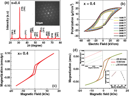
Figure 1. PZTFT x = 0.4 multiferroic material: (a) x-ray diffraction patterns and selected area electron diffraction (SAED) patterns show single-phase material; (b) ferroelectric and (c) ferromagnetic hysteresis loop showing multiferroic behaviour; (d) electric control of magnetisation, linear ME coupling (lower inset) and change in remanent magnetisation under an external field (upper inset). Adapted from [39], reproduced with permission (© 2011 AIP).
Download figure:
Standard image High-resolution image
Figure 2. (a) The ferroelectric domain configurations change dramatically with an applied magnetic field (scale bar, 2 μm). Adapted from [43], reproduced with permission. (b) Images of the ferroelectric domain states after the application of successive electric and magnetic fields; amplitude and phase maps have been superimposed onto each other. Yellow is associated with the polarisation components pointing to the left of the images and pink to the right. The remanent states have been imaged after sample exposure to the following succession of bias voltages/magnetic fields: (i) −25 V, (ii) +25 V, (iii) −25 V, (iv) +3 kOe, (v) −3 kOe, and (vi) −25 V. Adapted from [44], reproduced with permission.
Download figure:
Standard image High-resolution imageControl of ferroelectric domains using magnetic field in (PbZr0.53Ti0.47O3)(1−x)–(PbFe0.5Ta0.5O3)x
Evans et al [43] showed a significant change in the ferroelectric domains of PZTFT lamella taken from a ceramic grain using the focussed ion beam technique (FIB) under a moderate external magnetic field using lateral piezoresponse force microscopy (LPFM). The images in figure 2(a) present results before (upper) and after (lower) the application of the 18-kOe (1.8 T) magnetic field; a clear change in ferroelectric domain states is observed. The LPFM amplitude images of the same region of the PZTFT single-crystal lamella (the left and middle panels) show variations in the local in-plane piezoelectric activity under the magnetic field. The domains or packets of domains and domain walls are clearly visible, and their orientations are distinct. Various cantilever orientations were used to scan the LPFM images; tip geometries are shown schematically in blue. The right-hand side images in figure 2 are the in-plane PFM phase signal deduced from the amplitude images. Various local polarisation directions are mapped and shown in the right-hand panels. The directions of the local polarisations are shown for all four quadrants (grey: left and up; lime green: left and down; purple: right and up; brown: right and down). Ferroelectric domains were preferentially grown in the left and down direction (lime green) under the application of external magnetic fields. These results successfully demonstrate strong and explicit ME coupling at the nanoscale for ferroelectric domains where these domains switch with moderate magnetic fields at room temperature.
In a subsequent experiment Evans et al examined the behaviour of ferroelectric domains on the same PZTFT single-crystal lamellae with capacitor structure under the application of both electric and magnetic fields [44]. Figure 2(b) shows the domain configurations and their magnitude after the application of successive electric fields (blue and green arrows) ((i) −25 V, (ii) +25 V, (iii) −25 V). A consistent change in in-plane domain orientations and magnitudes was observed under E-fields, which can be easily switched back and forth under E-fields. The application of a magnetic field ((iv) +3 kOe) efficiently switched the electric polarisation; however, the reversal of the magnetic field ((v) −3 kOe) shows only a modest change in the ferroelectric domains (see figure 2(b) upper). These authors quantified the domain changes by counting the 'yellow' phase pixels in each image (see figure 2(b) lower). The changes in the populations of domains (yellow phase) are shown in the lower portion of figure 2(b) for various successive bias voltages and magnetic fields. It is remarkable that a magnetic field applied perpendicular to the PZTFT lamella can induce the switching of the ferroelectric domains, which is comparable to that produced by electric fields—clearly there is significant room-temperature magnetoelectric coupling, but magnetic switching fatigues easily.
Recently two theoretical works were published related to PbZr0.53Ti0.47O3)(1−x)–(PbFe0.5Ta0.5O3)x (PZTFT) and (PbZr0.53Ti0.47O3)(1−x)–(PbFe0.5Nb0.5O3)x (PZTFN) single-phase multiferroic magnetoelectric materials. Morozovska's group [79] published a theoretical study in which they presented a phase diagram for PZTFT and PZTFN materials. They established the boundaries between paraelectric, ferroelectric, paramagnetic, antiferromagnetic, ferromagnetic and magnetoelectric phases. However, their predicted dome structures are not confirmed experimentally. On the other hand, Kuzian et al [80] proposed that the room temperature magnetism in these systems can be due to the existence of regions with a special chemical order that results in the ordered spins of antiferromagnetic interacting Fe3+ S = 5/2 spins.
Bulk composite multiferroics
In order to compensate the deficiencies of the natural multiferroics at ambient temperatures the fabrication of artificial multiferroics to enhance magnetoelectric effects opens up the possibility of tailoring the properties using two different compounds, one being ferromagnetic and other being ferroelectric [8, 26]. The aim of this technique is to create materials that display both properties of the parent compounds and their cross coupling, but the cross coupling is generally indirect via strain (magnetostriction plus electrostriction and/or piezoelectricity) and not direct polarisation-magnetisation (MP) interaction. A magnetic field applied to the composites will induce magnetostriction, which produces piezoelectric and/or electrostrictive responses. This ME property of the ferroelectric-ferromagnetic composite is known as a product-property of the composite [81]. The ME composites could have various connectivity schemes, but the common connectivity schemes are: (i) 0-3 type particulate composite where the piezoelectric/magnetic particles are embedded in a matrix of magnetic/piezoelectric phases; (ii) 2-2 type laminate ceramic composites consisting of the piezoelectric and magnetic oxide layers; and (iii) 1-3 type 'fibers' of one phase embedded in the matrix of another phase [8]. The composite structures open up new avenues for tailoring the ME response through the choice of phase properties, volume fraction, shape, connectivity and microstructure of the constituents. The room-temperature ME coupling coefficients of composite structures have been found to be at least three to five orders of magnitude higher than ME coupling for single-phase compounds [75]. This idea was initially developed in the ceramic-composite (0-3 type) [82–102], and later laminated multilayers were investigated [103–114].
The first work on the ME composite was done at the Philips laboratory [82–85] the ME composites were prepared by the unidirectional solidification of a eutectic composition of the quaternary system Fe–Co–Ti–Ba–O; the ME coefficient is  = 130 mV cm−1 Oe−1 [82–84], which is superior to that of single-phase materials such as Cr2O3. In 1978 they reported on the sintered ME composite of BaTiO3 and Ni(Co,Mn)Fe2O4 with excess TiO2 in terms of the particle size effect, the cooling rate and the mole ratios of both phases [84]. After the pioneering experiment on BTO/CFO [82–85], a variety of ferroelectric/ferrite bulk compositions werefabricated consisting of ferroelectric phases such as BaTiO3 (BTO), PbZr1−xTixO3 (PZT), PbTiO3 (PT), polyvinylidenefluoride (PVDF) and ferromagnetic phases such as CoFe2O4 (CFO), Tb1−xDyxFe2-Terfenol-D, NiFe2O4 (NFO), CuFe2O4 (CuFO) and LaMnO3 (LMO). Although bulk composite materials were considered to exhibit promising (larger) ME effects, so far the observed ME coefficients in ceramic composites are ten times lower than theoretical calculation, which is mainly due to their inherent fabrication problems, such as atomic scale interfacial diffusion during the growth process, chemical reactions between the constituent starting materials during sintering processes, or the interdifusion of the phases. However, important efforts have been made to obtain the desired properties of individual constituents such as ferroelectric (good piezoelectric, high electromechanical coupling coefficients) and ferrite phases (good piezomagnetic, high magnetomechanical coupling coefficients, high resistivity), as well as the improvement of parameters related to the composite materials, via carefully chosen constituent materials, sintering processes, grain size, mole ratios, thermal expansion, mismatch between phases and the uniform distribution of the magnetostrictive phase within a piezoelectric matrix.
As a good example, Ryu et al [100] published an improvement of ME properties with a more homogeneous dispersion of the magnetostrictive phase (Ni0.8Zn0.2Fe2O4) into a piezoelectric matrix 0.9Pb(Zr0.52Ti0.48)O3–0.1Pb(Zn1/3Nb2/3)O3 (see figures 3(a) and (b)) and Ramanaa et al [99] synthesised Ni0.83Co0.15Cu0.02Fe1.9O4 (NCCF)/PZT; they added Co and Cu to NiFeO3 to increase the resistivity of the ferrite phase (NCCF), obtaining a maximum ME coefficient of 3.15 V cm−1 Oe−1 in the composite containing 0.5NCCF + 0.5PZT, as shown in figure 2(c). Due to the improved engineering process, a viable ME response can be observed in multiferroic ME composites above room temperature. Various ME bulk composites in different systems have been investigated; the first part of table 2 shows the list of some bulk composite that have been investigated over the last forty years.
Table 2. Composite multiferroic materials.
| Composite multiferroic | ||||
|---|---|---|---|---|
| Material | Characteristic | Examples | α (mV cm−1 Oe−1) | Ref. |
| Particulate ceramic composite | A variety of ferroelectric/ferrite compositions have been fabricated consisting of the ferroelectric phases, such as BaTiO3 (BTO), bZr1−xTixO3 (PZT), polyvinylidenefluoride (PVDF), PbTiO3 (PT) and ferromagnetic phases such as CoFe2O4 (CFO), Terfenol-D (Tb1-xDyxFe2), NiFe2O4 (NFO), CuFe2O4 (CuFO), LaMnO3 (LMO), | BTO/CFO | 130 | [82–85] |
| CuFO/ BTO | 425 | [86, 87] | ||
| CFO/ BTO | 200 | [88] | ||
| PZT/CFO | — | [89] | ||
| Pb0.95Sr0.05Ni0.06 Zr0.49Ti0.40O3/CFO | 70 | [90] | ||
| NFO/PZT | 80–115 | [91–92] | ||
| BTO/LMO | — | [93] | ||
| Terfenol-D/ PVDF | 1430 | [94] | ||
| BTO/Ni0.94Co0.01Cu0.05Fe2O4 | 0.64 | [95] | ||
| Sr0.5Ba0.5Nb2O6/CFO | 25 | [96] | ||
| ErMnO3/La0.7Sr0.3MnO3 | — | [97] | ||
| CFO–BiFeO3 | 285 | [98] | ||
| Ni0.83Co0.15Cu0.02Fe1.9O4/PZT | 3150 | [99] | ||
| 0.9Pb(Zr0.52Ti0.48)O3–0.1Pb(Zn1/3Nb2/3)O3–Ni0.8Zn0.2Fe2O4 | 75 | [100] | ||
| (Ba0.8Ca0.2TiO3)x–(Ni0.2Cu0.3Zn0.5Fe2O4)1−x | 280 | [101] | ||
| 0.5CFO–0.375Pb(Fe2/3W1/3)O3–0.125PT | 70 | [102] | ||
| Laminated composite | The mechanical stress mediating between the electrical and magnetic properties of the composite should be passed through the constituents with losses as low as possible. These obstacles were overcome in 2001 by using laminar instead of particulate composites. | PZT/NiFe2O4 (bilayer) | 20, 460T-45L | [103–105] |
| PZT/NiFe2O4 (multilayer) | 1500 | [104] | ||
| PZT-CFO | 55T-5L, | [105, 106] | ||
| PZT/La0.7Sr0.3MnO3 | 60T-20L | [107] | ||
| PZT/La0.7Ca0.3MnO3 | 15T,5L | [103] | ||
| Terfenol-D (T)-PVDF/PZT(P)-PVDF/T | 3000–4000 | [108, 109] | ||
| T/P/T | 6000 | [110] | ||
| PZT rod arrays embedded in Terfenol-D | 6000 | [111] | ||
| PZT/ Terfenol-D discs | 4680 | [112] | ||
| PVDF-hexafluoropropylene-Metglass | 12 000 | [113] | ||
| Al(NO3)3·9H2O doped Poly(vinylidene fluoride-co-hexafluoropropylene) | 22 000 and 320 000 (68 kHz) | [114] | ||
| P(VDF-HFP)-Metglass | ||||

Figure 3. (a) Backscattering emission image obtained by SEM for the PZT–PZN-NZF composite sintered at 1200 °C for 2 h with different NZF ball-milling times. (b) Magnetoelectric properties (dE/dH) of the PZT–PZN–NZF composite sintered at 1200 °C for 2 h. Adapted from [100], reproduced with permission (© 2011 The Japan Society of Applied Physics). (c) ME voltage coefficient as a function of applied dc magnetic bias field for the composites (1−x)PZT–xNCCF. Adapted from [99], reproduced with permission (© 2009 Elsevier).
Download figure:
Standard image High-resolution imageLaminated composite multiferroics
In spite of all these efforts, the considerable enhancement of the composite ME response beyond ~3000 mV cm−1 Oe−1 has not been attained after almost four decades of research, and the observed ME coefficients are less than 1-2 orders of magnitude compared with the theoretically predicted values. Several reasons for this discrepancy were already mentioned. The ME properties of the composite materials were not good enough to be used in memory applications but were useful in magnetic field sensors. Using laminar composite materials instead of particulate composites overcame some problems and several researchers have claimed that they were able to operate nano-tesla (nT) magnetic field sensors [8, 25].
Laminated composites have much higher ME coefficients than those of single-phase materials or particulate composites. Another remarkable difference between the laminated and particulate composite ceramics is that the laminated structures exhibit a much larger anisotropy than the particulate ones [8]. ME couplings have been studied experimentally [82–114] and theoretically [81, 115, 116]. Potentially, these new materials and structures can be used for magnetic field sensors, current sensors, energy harvesters, transformers and ME filters, as well as phase shifters. In laminated composites the ME response strongly depends on the interfacial bonding between two layers, since the mechanical stress mediating the dielectric and magnetic properties of the composite should be passed through the constituents with losses as low as possible. Throughout the years various efforts have been made to improve the ME coefficient values in laminar composites, and these efforts have been directed to the preparation techniques of the samples, the choice of materials, and the different structures and thicknesses of the samples. Initially the technique used to fabricate the laminated composites was conventional sintering; however, in order to suppress inter-diffusion and chemical reaction of the constituents and to improve the quality of the laminate composites, a hot pressing technique was employed, i.e. Nan's group reported an increase in the ME coefficient up to 6000 mVOe−1 cm−1 when the Terfenol-D-PVDF/PZT-PVDF/ Terfenol-D-PVDF (T/P/T) layer structures were fabricated using a hot molding press (see figure 4) [108, 110].
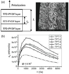
Figure 4. (a) Schematic illustration and typical micrograph of the fractured surface of the laminated TPT composites. TFD denotes Terfenol-D. (b). The ME sensitivity αE values measured at resonance frequency ( f r) for the laminated composites as a function of the bias magnetic field at the measuring angle θ = 90°. In the legend the labels 1,2,3,4,5 correspond to 1/7, 2/7, 3/7, 4/7, 5/7 (tp/L) ratios, respectively, for various TPT laminated samples. Adapted from [110], reproduced with permission (© 2005 APS).
Download figure:
Standard image High-resolution imageDifferent types of material can be used in the fabrication of ME laminate composites, i.e. hard materials such as piezoelectric (PZT, BTO) and piezomagnetic (NFO,CFO, LSMO, LSCO) ceramics; or soft materials, for piezomagnetics Metglass and Terfenol-D (TbxDy1−xFe2 (x ~ 0.3)); and for piezoelectric polymers, we have polyvinylidenefluoride (PVDF), P(TrFE). Large ME responses have been obtained with a combination of hard and soft materials in the laminated composite.
The most commonly studied laminated composite structure is the 2-2 structure of bilayers or multilayers [103–107]; however, quasi-2-2 structures can be obtained in the cases of terfenol-D-polymer (PVDF) and PZT–polymer (PVDF). In this case the PVDF polymer is used just as a matrix binder [108–110]. Another important structure is 1-3; Shi et al [111] used a dice-and-fill process to prepare 1-3 type multiferroic composites in which the bulk PZT is staked into a PZT rod array, and the gaps between the rods are filled with a mixture of terfenol-D particles and epoxy. Later, the epoxy hardens and connects the PZT-terfenol-D composite structure in the form of a pseudo 1-3 multiferroic composite. Recently, large ME coupling (12 000 mVOe−1Cm−1) was achieved in PVDF-hexafluoropropylene-Metglass fabricated by an extrusion-blown and hot-pressed quenched method; an additionally interesting phenomenon—a field-induced phase transition—was observed in this system (see figures 5(a) and (b). Recently, Jin et al [114] fabricated a 2-2 structure of Al(NO3)3·9H2O doped poly(vinylidene fluoride-co-hexafluoropropylene) P(VDF-HFP) and Metglass as ferroelectric and ferromagentic phases. First, they improved the ferroelectric characteristic of P(VDF-HFP): adding Al(NO3)3·9H2O promoted the presence of hydrogen-bonding between O-H from Al(NO3)3·9H2O and C-F from P(VDF-HFP), which increased the polarisation ordering of the ferroelectric polymer; and second, they improved the crystallisation by annealing (80%) compared with the pristine P(VDF-HFP). The highest value of the ME coefficient of the laminate composite P(VDF-HFP)/ iron-based metglass was found to be 22,000 mV cm−1 Oe−1, and a colossal αME of 320 000 mV cm−1 Oe−1 was obtained at a frequency of 68 kHz, which was attributed to the electromechanical metal used to improve the ferroelectricity due to the resonance enhancement of the elastic coupling interaction between the ferroelectic polymer and metglass layers.
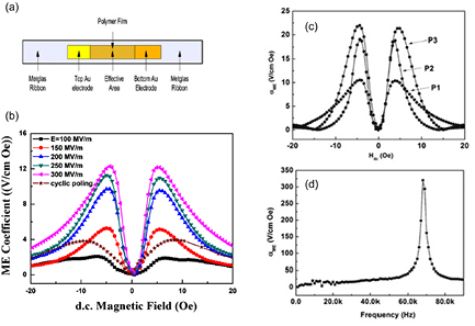
Figure 5. (a) Schematic configuration of P(VDF-HFP)/Metglas laminate. The polymer film was smaller in area than the Metglas and placed in the central area, optimising the magnetic flux effect. (b) ME coefficient of hot-pressed P(VDF-HFP)/Metglas laminates as a function of a dc magnetic field for conventional poling. The ME coefficient versus the dc magnetic field for cyclic poling (Ep = 225 V m−1 for extruded film). Adapted from [113], reproduced with permission (© 2011 AIP). ME voltage coefficient of the Al(NO3)3•9H2O doped Poly(vinylidene fluoride-co-hexafluoropropylene) P(VDF-HFP)-Metglass composites as a function of: (c) dc magnetic field and (d) frequency range from 0–90 kHz. Adapted from [114], reproduced with permission (© 2014 Wiley-VCH).
Download figure:
Standard image High-resolution imageA list of several laminated composites appears in table 2 with their respective ME coefficient values, emphasising the superior ME coefficient values obtained in laminar composites compared with ceramic composites and single crystals.
Single and heterostructure thin films
The advances in thin-film growth techniques have provided a controlled way of synthesising high quality single-phase and nano-structured thin films and have allowed the properties of existing materials to be modified by strain engineering [25, 117]. On the other hand, nano-structuring is a promising approach that has opened the door to the design of practical devices based on ME coupling. Multiferroic single-phase and nano-structured thin films have been produced using a wide variety of growth techniques, including sputtering, spin coating, metal-organic chemical vapor deposition (MOCVD), sol–gel processing, pulsed laser deposition (PLD), molecular beam epitaxy (MBE) etc. Research interest in magnetoelectric multiferroic thin films has been increasing over the last decade, due to the new range of phenomena observed, such as emergent phenomena at multiferroic hetero-interfaces [118], which have potential applications in micro-devices and integrated units such as micro-sensors, micro-electro mechanical systems (MEMS) and high-density information storage [2]. In the case of single-phase thin-film multiferroics, most of the published work is devoted to hexagonal manganites such as YMnO3 (YMO) [4, 119–129] and Bi-based perovskites (mostly pure or chemically doped BiFeO3) [130–143]; another series of single-phase materials are solid solutions of lead-based perovskitse [37, 144–146] ME materials.
Single-phase multiferroic thin films
Although composite layers of ferromagnets and ferroelectrics make excellent devices as transducers, actuators and low magnetic field detectors (comparable to SDQUIDs), their speeds are generally unknown and apt to be slow, since their elastic coupling is limited by the speed of sound (ferroelectric domain wall speeds cannot be supersonic, although magnetic walls can be). Thus, they are unlikely to be useful as multiferroic magnetoelectric random access memories. Moreover, they are unlikely to be useful for voltage-controlled magnetic tunnel junctions (MTJs), since the total thickness of a tunnel junction must be <6 nm, and interfaces greatly reduce tunneling currents. Thus, artificial superlattices and FE/FM layer structures are not promising for two important classes of magnetoelectric devices: These require single-crystal or single-phase epitaxial film multiferroics.
Yttrium manganite, YMnO3 (YMO): this ABO3 oxide belongs to the RMnO3 (R = rare-earth element) system, which can be divided into two subsystems in which the crystal structure is mainly determined by the size of the R cation. For a larger R size (R = La, Dy) an orthorhombic perovskite structure is adopted, whereas for a smaller R (R = Sc, Y,Ho, Lu) the structure is hexagonal. One of the typical rare-earth manganites studied in thin-film form is YMnO3; its structure can be hexagonal (ferroelectric) or orthorhombic (non-ferroelectric) depending on the epitaxial strain. Hexagonal YMO undergoes a paraelectric-ferroelectric phase transition at Tc ~ 900 K, and it displays an antiferromagnetic transition around 70 K. That is, YMO is a room-temperature ferroelectric and low-temperature multiferroic [119]. Aken et al [120] reported that the ferroelectricity mechanism in YMO is driven entirely by electrostatic and size effects (dipole-dipole interaction and oxygen rotations), rather the usual changes in chemical bonding associated with FE phase transition in perovskite oxide; although a corrected and complete analysis of the phase transitions sequence of YMO with the possible existence of intermediate phases, i.e. P63mc (FE) and P63 /mcm (paraelectric) between P63cm (FE) and P63/mmc (paraelectric), was reported subsequently by Fennie and Rabe [121]. The FE thin films are expected to be more suitable dielectric materials for metal-ferroelectric-semiconductor field-effect transistor (MFSFET) structures due to the absence of volatile components such as Pb, Ti or Ta, which can easily diffuse into semiconductors. Fujimura et al [4] proposed YMnO3 thin films as a new candidate for nonvolatile memory devices, using rf magnetron sputtering. They fabricated epitaxial (0 0 0 1) YMnO3 films on (1 1 1) MgO, (0 0 0 1)ZnO : Al/(0 0 0 1), sapphire, and polycrystalline films on (1 1 1)Pt /(1 1 1)MgO. The dielectric properties of the epitaxial and polycrystalline YMnO3 films were almost the same. After Fujimura's publication in 1996, YMO thin films were synthesised via a wide variety of substrates and growth techniques [117]. Lee et al [122] used rf sputtering to grow c-axis oriented Pt /YMO/Y2O3/Si and Pt/YMO/Si—that is, metal/ferroelectric/insulator/semiconductor (MEFIS) and metal/ferroelectric/ semiconductor (MFS) structures, respectively. Electrical properties showed the memory window of the MEFIS is greater than that of the MFS capacitor. Later, Yoo et al [123], using the same growth technique and substrate utilised in reference 124, found that c-axis/polycrystalline (bi-layer) YMO thin films showed a better memory window than both purely c-axis oriented and purely polycrystalline YMO thin films. Epitaxial (0 0 0 1) YMO thin films on (1 1 1)Pt/(0 0 0 1)sapphire (epi-YMO/Pt) and Y2O3/Si (epi/YMO/Si) and YMO oriented polycrystalline films on (1 1 1)Pt/ZrO2/SiO2/Si were grown by using the PLD technique [124]; excellent ferroelectric properties were obtained in epitaxial films compared to oriented polycrystalline films. The crystallinity and CV hysteresis of the epi-YMO/Pt and epi/YMO/Si thin films were almost the same. Epitaxial YMO thin film is a ferroelectric material suitable for MEFIS applications. Dho et al [125] found that the growth orientation and surface morphology of YMO films were sensitively dependent on the substrate (lattice mismatch) and deposition conditions (oxygen background pressure); that is, for (1 1 1) SrTiO3 (STO) substrates, the orthorhombic YMO phase competes with the hexagonal phase, which was induced by the strong compressive stress. YMO thin films were also synthesised by sol–gel processes using alkoxides on Pt(1 1 1)/Ti/SiO2/Si [126]. It was found that higher sintering temperatures improve the ferroelectric polarisation and crystal crystallinity with preferential orientation. The highly c-axis oriented YMnO3 thin films illustrated higher remanent polarisation (2Pr = 3.6 μ cm−2) compared with polycrystalline YMnO3 thin films. More recently, Uusi-Esko et al [127] used atomic layer deposition (ALD) to grow both the hexagonal and orthorhombic forms of YMnO3. On Si(1 0 0) substrates the product was the hexagonal phase of YMnO3; whereas on LaAlO3(1 0 0) and STO (1 0 0) substrates, the metastable orthorhombic YMnO3 phase was formed. Foncuberta's group [128] grew orthorhombic epitaxial YMO [0 0 1] (c-axis) and [1 0 0] (a-axis) textured films on conducting Nb : STO substrates. They showed a bc-cycloidal magnetic order (bc plane) exists in YMnO3 thin films and can be switched to ac-cycloid (ac plane, where a, b and c represent the directions of the x-, y-, z-axes)) by an appropriate magnetic field. This finding showed that a non-collinear spin arrangement in thin films allows switchable electrical polarisation and tunability of their dielectric response by magnetic fields; however, these experiments were carried out at 5 K. Finally, Wadati et al [129] fabricated thin films (40 nm) of YMnO3 on a YAlO3 (0 1 0) substrate by PLD. They reported two successive commensurate and incommensurate magnetic phase transitions below 35 K and 45 K, respectively, suggesting the existence of E-type cycloidal states. These results suggest that the large polarisation below 35 K was mainly due to the presence of magnetic ordering in epitaxial thin films. These films show highly correlated spin-electric polarization phenomena below 35 K, make them suitable candidates for next generation ferroelectric-gated field-effect FETs [122]. However, the high fabrication temperature (⩾800 °C) makes it impractical for integration into silicon technology [4, 119–128]. Further studies to achieve robust ferroelectric properties and room-temperature multiferroicity in manganites are pending.
Bismuth ferrite, BiFeO3 (BFO)
The single-phase multiferroic that has been most studied in the last decade is BFO due to its multiferroic and potential magnetoelectric properties. BFO is a fully recognised room-temperature multiferroic that has all three ferroic order parameters—ferroelectric/ferroelastic (Tc = 1103 K) [130], antiferromagnetic (TN = 643 K) [131]—and exhibits weak ferromagnetism at room temperature; however, the cross coupling between these ferroic parameters in single-phase form is very weak and poorly understood. Bulk BFO single crystals possess a rhombohedral perovskite structure (a = b = c = 5.63 Å, α = β = γ = 59.4°) [132]. In single-crystal form an early report found the spontaneous polarisation is ~6.1 μC cm−2 along the (1 1 1) direction at 77 K [133], but this is known now to have simply been a poor sample. The ferroelectricity in BFO is due to the stereo-chemically-active 6s lone pair of Bi3+. Studies during the 1980s indicated the magnetic nature of BFO is a G-type antiferromagnetic order, wherein Fe3+ ions are surrounded by six neighbouring Fe3+ ions with spin anti-parallel to the central ion [134]. The symmetry also allows a canting of the antiferromagnetic sublattices, resulting in a macroscopic magnetisation 'weak ferromagnetism' [135]. In 2002, Palkar et al [136] reported weak ferroelectric properties in BFO thin films deposited on a Pt/TiO2/SiO2/Si substrate, and magnetoelectric properties were demonstrated by an anomaly in the dielectric constant in the vicinity of the Néel temperature; later, Yun et al [137] using the same substrate and technique as Palkar but lower oxygen pressure during deposition (0.01–0.1 Torr), obtained good current-voltage characteristics and an improvement in ferroelectric properties, high remanent polarisation (Pr), 2Pr ~ 71.3 μC cm−2 and coercive field (Ec), 2Ec ~ 125 kV cm−1. However, in 2003 Wang et al [25] reported epitaxial monoclinic BFO thin films grown on SrRuO3/STO(1 0 0) substrates by PLD, with a surprisingly large electric polarisation response up to 2Pr ~ 120 μC cm−2, which is one order of magnitude higher than the value of 6.1 initially reported from bulk BFO single crystal [130, 133]. These films also show enhanced thickness-dependent magnetism compared to the bulk, which is attributed to the mismatch strain induced by heteroepitaxy. This study has led to a growing interest in BFO thin films, which has endured until the present day, almost a decade after its publication. Later, Li et al [138] investigated the effects of the orientation of the STO substrate on crystallography and the ferroelectrical properties of BFO. BFO films grown on (1 1 1) had a rhombohedral structure like single crystals; whereas films grown on (1 0 1) or (0 0 1) were monoclinically distorted from the rhombohedral structure, attributed to the epitaxial constraint; the remanent polarisation in each case was 55, 80 and 100 μC cm−2, respectively. Afterwards, a multilayer film of BiFeO3/La0.7Sr0.3MnO3/SrTiO3 was deposited on a Si substrate by pulsed laser deposition. The BiFeO3 film showed a low leakage-current density, and 2Pr ~ 110 μC cm−2 was observed at room temperature [139] On the other hand, Shvartsman et al [140] showed large ferroelectric polarisation ~40 μC cm−2 in ceramic BFO, a value close to the theoretically predicted value. Since the highest values of polarisation were obtained in ceramic, polycrystalline and epitaxial films, these results indicated the larger polarisation is not related to the strain but it is an intrinsic property of BFO, a result supported by first-principles calculation [141].
However, the major drawbacks for the BFO device are high leakage current, a tendency towards fatigue and thermal decomposition near the coercive field, which have been addressed by doped BFO, for example with Pr or Mn doping [142, 143]. Due to its exceptional ferroelectric properties, multiferroic nature, potential ME coupling and lead-free character, BFO remains a potential candidate for the next generation of ferroelectric memory applications. Recently Sando et al [144] reviewed work on BiFeO3 epitaxial thin films, where they discussed the ferroelectric properties and ferroelectric photovoltaic response in strained or doped thin films, the correlation between strain, magnetic spins and electric polarisation, wide range optical properties, optical dielectric response, bandgaps, photovoltaic effects, and advances in the design of prototype devices for electronics, spintronics and photonics.
Lead-based solid solution perovskites
Another multiferroic single-phase material family very recently studied in thin-film form are lead-based solid solution perovskites (SSPs). To our knowledge the first publication on Pb-SSP thin films was from Ashok et al [37]. They reported single-phase polycrystalline (PbZr0.53,Ti0.47O3)0.8–(PbFe0.67W0.33O3)0.2, (0.8PZT/0.2PFW) synthesised by chemical solution deposition, a new room-temperature single-phase multiferroic magnetoelectric material. Later, the multiferroic properties of the single-phase 0.8PZT/0.2PFW system were confirmed by Lee et al [145, 146] by growing epitaxial 0.8PZT/0.2PFW films on a SRO coated STO (0 0 1) substrate. And (PbZr0.53Ti0.47O3)0.60–(PbFe0.5Ta0.5 O3)0.4, (0.6PZT/0.2PFT) highly oriented thin film was synthesised by PLD on La0.67Sr0.33CoO3 coated MgO substrates. These films show near room temperature a frequency dependent dielectric maximum, moderate polarisation and a weak magnetic moment, as well as multiferroic relaxor characteristics [147]. The synthesis of single-phase solid solution materials using conventional and relaxor ferroelectrics might open a new way to realising a room-temperature multiferroic material with strong magnetoelectric coupling.
Multiferroic nano-composites: nomenclature
A short summary of multiferroic (ferromagnetic-ferroelectric) nano-composites is given below, including multiferroic superlattices, multiferroic bi-relaxors with only short-range ordering of magnetisation and electric polarisation, and ferroelectrics with long-range ordering but short-range magnetic clustering. Although these structures can be described with the usual two-digit notation (e.g. 0-3 or 1-3, where the first digit is the dimensionality of the first phase and is chosen as less than or equal to that of the second phase, which defines the connectivity), an additional digit or subscript is necessary to discriminate between short- and long-range ordering.
The physics of composite materials is successfully categorised into classes with two-digit labels, such as 0-3, in which each digit can be from 0 to 3, the first digit describes the dimensionality of object within a matrix, and the second describes the dimensionality of its connectedness to other equivalent objects. For example, 1-3 describes a system with 1D rod-like objects (such as carbon fibers) connected to each other by a 3D matrix, such as a polymer or epoxy. For piezoelectric composites, the piezoelectric phase is conventionally designated by the first digit, even if it is the larger (e.g. 3-1 rather than 1-3), which is rarely the case [148]. This problem becomes acute only for multiferroic nano-composites, where the average size of the smaller phase can be only a few unit cells. In this case there are no grains or grain boundaries and there is a grey area between composites and relaxors.
These notations do not completely specify the geometry of the system; for example, the labels do not discriminate between oriented, aligned rods within a matrix and randomly oriented rods ('PZT spaghetti'). Nan et al [8] published an excellent review of multiferroic composites. The present aim is merely to suggest some convenient notation for these new families of important materials, for example:
- (i)2-2 systems: 2-2 composites are generally the choice for tape-cast multilayer actuators, such as PZT composites. They also include most multilayer capacitors [8]. Within the class of 2-2 multiferroic composites we have examples in which both magnetic and ferroelectric ordering are long range (Terfenol-D on PZT [149] or BaTiO3 on Ni [150])—we will denote them and similar cases [151] as 2L–2L and those birelaxors such as PbFe2/3W1/3O3 in which both magnetic and ferroelectric ordering are short range and probably planar [18, 37, 152]—which we denote as 2S–2S.
- (ii)1-3 or 3-1 systems: most piezoelectric devices are 1-3 systems, as developed initially by Newnham and Cross and their Penn State group [141]. 3-1 multiferroic composites were pioneered by developments of nano-pillars of cobalt ferrite in barium titanate [153] Here the magnetic and ferroelectric ordering is both long range, and we denote it as 3L–1L.
- (iii)0-3 systems: compounds such as Pb(Fe,Ta,Zr,Ti)O3 [39] or PbFe1/2Ta1/2O3 [24, 154] or PbFe1/2Nb1/2O3 [155] are nano-composites although they are nominally single phase. This apparent paradox arises because the Fe ions cluster at the B-site and are not in random occupancy. This produces a point-like 0D object with 3D connectivity through the surrounding medium. We designate this as 0S–3L, meaning that the ferroelectricity is long range but the magnetism is short range.
Heterostructure composite thin films
During the last decade, much effort has been made to synthesise multi-phase thin films composed of materials that have large ferromagnetic and ferroelectric ordering, with the possibility of ME coupling. A new level in design and development in multiferroic thin films has been achieved due to improved first-principles computational techniques. The advancement of both experimental fabrication processes and theoretical modeling codes and parallel processing among theoretical and experimental scientists has aided in the design of new magnetoelectrics with larger coupling parameters [1, 156, 157]. Advanced growth techniques make it possible to fabricate ultra-thin films with various ferroelectric and ferromagnetic phases, together with atomic-level connections between the FM and FE layers [2]. The availability of high quality thin-film samples and their characterisation using highly sophisticated equipment and the precise measurement of ME coupling coefficients have both opened the door to the design of practical devices based on ME coupling. From a microstructural point of view the composite thin films can classified as 0-3 particulate nanocomposite, 2-2 horizontal heterostructures and 1-3 vertical heterostructures, as was explained in more detail in the previous section.
From table 3 we can see the most studied configuration in multiferroic magnetoelectric thin film form is 2-2 as bi-layers, multilayers and superlattices for a diverse group of ferroelectric and magnetic materials. The popularity of the 2-2 configuration is due to their ease of synthesis along with a reduced leakage problem due to the blocking of the current flow by resistive ferroelectric layers. Despite the nature of multiferroics, indirect ME coupling has been observed in different ways in 2-2 structures, and evidence of direct coupling ME is absent in most of them. On the other hand, the ME values reported in thin-film form are lower compared with those reported in ME laminated composites (see table 2). Although many of the film growth techniques allow better control of the interfaces that improve the transfer of the strain efficiency between two phases, the ME coupling in the 2-2 configuration is affected by the a large in-plane constraint from the substrate.
Table 3. Multiferroic heterostructures thin films.
| Thin films heterostructures | ||||
|---|---|---|---|---|
| Structure | Materials | Technique | α (mV cm−1 Oe−1) | Ref. |
| Horizontal 2-2 | 2001 | |||
| La0.67Sr0.33MnOx/(Pb,La)(Ca.Ti)O3 | MOD- ML | MR | [158] | |
| 2004 | ||||
| BaTiO3 (BTO)/ CoFe2O4 (CFO) | Composition spread | — | [159] | |
| Pr0.85Ca0.15MnO3/Ba0.6Sr0.4TiO3 | PLD–SL | MR | [160,161] | |
| 2005 | ||||
| La1.2Sr1.8Mn2O7/PbZr0.3Ti0.7O3 | CSD | Dielectric anomaly | [162] | |
| La0.7Ca0.3MnO3/BTO | PLD–SL | MR, MC | [163] | |
| BiFeO3 (BFO)/ PbZr0.5Ti0.5O3 (PZT5) | CSD | — | [164] | |
| 2006 | ||||
| CFO/ PbZr0.52Ti0.48O3 (PZT) | PLD–ML | Magnetic field induces polarisation. | [165] | |
| La0.7Ca0.3MnO3/BTO | PLD–SL | MR | [166] | |
| CFO film/BTO single crystal subs | PLD | Magnetisation changes at | [167] | |
| PZT/CFO | PLD-ML | BTO phase transitions. Polarisation changes with magnetic field. | [168] | |
| 2007 | ||||
| La0.6Sr0.4MnO3/ 0.7Pb(Mg1/3Nb2/3)O3–0.3(PbTiO3) | PLD-SL | Polarisation changes with magnetic field. | [169] | |
| La0.67Sr0.33MnO3 (LSMO) /BTO sub | PLD | Magnetisation changes at BTO phase transitions. | [170] | |
| BFO/Bi3.25La0.75Ti3O12 | MOD-ML | — | [171] | |
| Fe/BTO substrate | MBE | Magnetisation changes at BTO phase transitions. | [172] | |
| PZT/LSMO | PLD | 4 | [173] | |
| PZT/CFO | PLD–ML | — | [174] | |
| 2008 | ||||
| PZT/SrRuO3/CoFe2O4 | PLD–ML | Polarisation and dielectric change with magnetic | [175] | |
| PZT/CFO | Sol–gel spin-coating BL | Magnetic induced voltage | [176] | |
| PZT5/CFO/PZT5 | Dual cathode rf sputtering | — | [177] | |
| Ni0.23Fe2.77O/Pb(Zr,Ti)O3 substrate | Spin spray deposition. Combined sol–gel and rf sputtering. | Magnetisation changes | [178] | |
| CFO/ PZT | Spin coating and rf sputtering | when applied electric field 238 | [179] | |
| BFO/CFO | rf sputtering -BL | — | [180] | |
| PZT/CFO | PLD–ML | — | [181] | |
| 2009 | ||||
| PZT/CFO | Sol–gel spin-coating BL | Magnetic field dependent Raman scattering | [182] | |
| PZT/ PbFe0.66W0.33O3 | PLD-ML | — | [183] | |
| PZT/CFO | PLD-ML | Magnetodielectric | [184] | |
| Bi2NiMnO6–La2NiMnO6 | PLD-SL | Magnetodielectric | [185] | |
| 2010—present | ||||
| PZT/LSMO | PLD–BL and SL | Dielectric anomaly, Polarisation changes with magnetic field. | [186–188] | |
| Ba0.7Sr0.3TiO3(BST) /LSMO | PLD-BL and SL | 250 | [151, 189, 190] | |
| PbZr0.65Ti0.35O3/ La0.5Sr0.5CoO3 | MBE-magnetron | — | [191] | |
| PbZr0.2Ti0.8O3/ La0.8Sr0.2MnO3 | Sputtering | Spin control by electric field. | [192] | |
| NiFe/BTO/SRO | PLD-BL | Electric field manipulated magnetization. | [193] | |
| BiFeO3/CoFe | CSD- sputtering | — | [194] | |
| Ni/[Pb(Mn1/3Nb2/3)O3]0.68–[PbTiO3]0.32 single crystal | E-beam evaporated (Ni) | Magnetoelectric manipulation of domain wall configuration. | [195] | |
| Fe/BaTiO3 single crystal | MBE | Magnetisation switching via interface lattice distortion. | [196] | |
| Ni/PZT | Sol gel-PZT and magnetron sputter-Ni | Electric voltage induced magnetisation. | [197] | |
| LSMO/0.7Pb(Mg2/3Nb1/3)O3–0.3PbTiO3 single crystal | rf sputtering | Large anisotropic remanent magnetisation tunability. | [198] | |
| La0.7Sr0.3MnO3/BaTiO3 BL | PLD | 169 at 1 kHz | [199] | |
| CoFe2O4–PbTiO3 ML | Sol–gel and spin coating | — | [200] | |
| CFO-PZT ML | Sol–gel | 227 | [201] | |
| BTO-BFO ML | PLD | 8760 | [202] | |
| Vertical 1-3 | 2004–2014 | |||
| BTO/CFO | PLD | Magnetisation changes at BTO phase transitions. | [153, 203, 204] | |
| CFO/PbTiO3 | PLD | — | [205] | |
| BFO/CFO | PLD-combinatorial method | — | [206, 207] | |
| BTO67-BFO33 | PLD | 20 750 | [202] | |
| Particulate nanocomposite 0-3 | 2003–2014 | |||
| Ba0.5Sr0.5TiO3 /BaFe12O19 | rf magnetron sputtering | — | [208] | |
| CFO/PZT | Sol–gel process | 317 | [209] | |
| BTO/CFO | PLD | — | [210] | |
| Bi3.15Nd0.85Ti3O12–CoFe2O4 | CSD | 35 | [211] | |
| BTO-Co | rf magnetron sputtering | 160–170 | [212] | |
| PZT/CFO | PLD | Magneto-capacitance | [213] | |
| CFO–PbTiO3 | Sol–gel and spin coating | — | [200] | |
Metal organic deposition, MOD; chemical solution deposition, CSD; pulsed laser deposition, PLD; molecular beam epitaxy, MBE; magnetoresistance, MR; magnetocapacitance, MC; bilayer, BL; multilayer, ML; superlattices, SL.
Since there are multiple factors that affect the magnetoelectric coupling in thin-film heterostructures: ferroelectric and ferromagnetic phases, substrate, heterostructure configuration-geometry etc, researchers are still trying to understand the underlying physics responsible for differences in the magnitude of ME coupling coefficients reported in the literature. For example: Li et al [199] studied the effect of substrates on LSMO/BTO bilayers and found the αME value at 1 kHz was higher on the STO substrate (263 mV cm−1 Oe−1) compared with the (LaAlO3)0.3(SrAl0.5Ta0.5O3)0.7 and LaAlO3–LAO (169 mV cm−1 Oe−1). This result is due to the strain induced by the lattice mismatch between BTO and LSMO films and larger interface coupling in the bilayer films deposited on the STO. Wang et al [200] investigated the effect of geometry (0-3 and 2-2 type) on the magnetic properties of CFO-PTO heterostructures. They obtained a reduction in magnetic moments of the 2-2 type compared with the 0-3 type and attributed this result to the formation of anti-phase boundaries due to compressive strain in CFO, which was larger in the 2-2 structure. Recently, Shi et al [201] synthesised the 2-2 structure of CFO-PZT for different volume fractions of CFO. They found that the αME coeficient increases with increased volume fraction of CFO in the layered films; the maximun αME observed was 227 mV cm−1 Oe−1.
A few years ago a series of experiments was conducted on bilayer samples where the thin-film layer of ferroelectric/ferromagnetic material had been grown on the ferromagnetic/ferroelectric substrate (single-crystal) film, which showed interesting magnetoelectric effects: i.e. Ni-PMN-PT, Ni presented a change in out-of-plane magnetisation due to the ME effect in this heterostructure [198]. A novel approach for magnetisation switching (magnetic anisotropy symmetry is altered) in Fe/BTO was observed when BTO changes from tetragonal to orthorhombic) [199]; large anisotropic remanent magnetisation was observed in LSMO/PMN-0.3PT structures, and the remanent magnetisation along the [1 0 0]/ [0 1 1] was suppressed/enhanced by an electric field applied to the substrate [201].
Because of the fabrication difficulty, fewer papers have been published for vertical 1-3 configurations (see table 3); in these systems the substrate clamping is expected to be less compared with 2-2 structures. Although these configurations show multiferroic properties, a direct measurement of the ME effect was presented only recently by Lorenz et al [202]. They fabricated both 1-3 and 2-2 structures of BTO-CFO on different substrates using puled laser deposition. The maximun αME obtained for BTO67/BFO33 1-3 structures reaches a maximum value of 20 750 mV cm−1 Oe−1 (20.75 V cm−1 Oe−1); in the case of multilayer films the maximun αME value was 8760 mV cm−1 Oe−1 (8.76 V cm−1 Oe−1). These values are the same order as reported for laminate composites. In contrast, the ME coupling in the 0-3 structure had been measured to range between 35–300 mV cm−1 Oe−1, but in most cases a leaky ferroelectric loop and high leakage current were reported in these structures. In their review article Nan's group [9] suggested additional confirmation is needed to determine whether the magnetic field-induced electric polarisation change in fact reflects real ME coupling in the composite films or artifacts.
Magnetic control of ferroelectric polarisation in PZT/LSMO bilayer structures
In an attempt to make artificial magnetoelectric multiferroic heterostructures, Dussan et al [186–188] synthesised Pb(Zr0.53Ti0.47)O3/La2/3Sr1/3MnO3 (PZT/LSMO) bilayer thin films on LaAlO3(1 0 0) (LAO) substrates using pulsed-laser deposition (PLD). Dielectric, ferroelectric, magnetic control of ferroelectric polarisation and electrical measurements were carried out on simple metal-insulator-metal (MIM) structures. The top platinum electrode was fabricated using dc sputtering using a shadow mask (see figure 6(a)) for the electrical and optoelectrical characterisation. They discovered polarisation suppression under the application of a moderate external magnetic field (0.34 T) which can be easily generated by a small coil induction coil beneath the electronic circuit. This effect occurred when the PZT layer thickness was ~550 nm (figure 6(c)); the hysteresis curve broadens remarkably with an increase in the applied magnetic field (H), and then vanishes completely at H = 0.34 T. This effect was completely reversible at room temperature. But it did not happen in the samples with a PZT thickness of around 1.4 μm (figure 6(b)). This result was explained in the light of the negative magnetoresistance effect of the LSMO, which becomes smaller in the applied H, increasing the current flow and hence the dielectric loss in the capacitor. The modest magnetic field (0.34 Tesla) quenched the ferroelectric polarisation (+P or −P to zero), thus generating strong interest in its usage in various sensors and electronics applications.
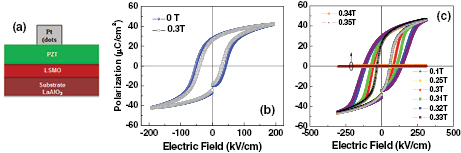
Figure 6. (a) A sketch diagram of the Pt/PZT/LSMO bilayer capacitor. (b) Ferroelectric hysteresis loops of 1.4 μm thick PZT film grown on LSMO coated LAO substrate; the effect of the external magnetic field was negligible. (c) 0.55 μm thick PZT film. A significant magnetic field dependence P-E loops were seen near a critical field of H = 0.34 T. Adapted from [188], reproduced with permission (© 2011 IOP).
Download figure:
Standard image High-resolution imageStrong magnetoelectric effect in Ba0.7Sr0.3TiO3/La0.7Sr0.3MnO3 (BST/LSMO) superlattices
Martinez et al [151, 189, 190] investigated the structural analysis and multiferroic and magnetoelectric properties of Ba0.7Sr0.3TiO3/La0.7Sr0.3MnO3 superlattice (SL) thin films grown on LaNiO3 (LNO) coated (1 0 0) MgO substrates by pulsed laser deposition. The thickness of the superlattice was kept constant (300 nm) irrespective of the modulation period in different SL-configurations. X-ray diffraction along with cross-sectional TEM of the (BST20uc/LSMO10uc)25 show that SL structure was present in the thin films (figure 7(a)). The direct ME measurement illustrates a strong response of superlattice films, figure 7(b) shows the typical ME response of one of these SLs: a maximum peak for αE,33 and αE,31 at ~250 Oe and ~90 Oe, respectively, was seen, which further decreases monotonically to zero with an increase in the bias magnetic field (H). A similar H-dependent behaviour of the ME coefficients was seen for the superlattices with other periodicities (i.e. Λ = 18, 24 and 36 nm). The experimental data fitted well to a modified free-body model, (solid lines in figure 7(b)). From figure 7(c), the ME values follow a hyperbolic behaviour which increases for the longitudinal (αE33) until Λ = 24 nm with further decrease in periodicities. A similar but inverse character is present in the case of the transverse ME coupling (αE31). However, the evolution of the ME coefficient as a function of periodicity requires further research on interface-microstructure-property relations; at present it is very poorly understood. These results showed the substrate clamping and the resulting weakening of ME coupling that are usually encountered in piezoelectric-magnetostrictive bilayers was not observed in the systems studied here. The ME voltage coefficients are in the range 35–300 mV cm−1 Oe for these MLs structures.
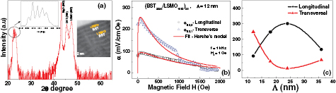
Figure 7. (a) X-ray diffraction pattern of a BST20uc/LSMO10uc SL on a MgO substrate. The upper inset shows the satellite peak around the (001) peak; the lower inset shows the transition electron microscopy (TEM) evidence of the formation of a superlattice structure. Longitudinal and transverse modes of magnetoelectric voltage coefficient (α): at 1 kHz and room temperature; (b) as a function of the bias magnetic field for (BST20uc/LSMO10uc)25 superlattices. The solid lines represent the fitting using the Harshe model; (c) as a function of the superlattices periodicity. Adapted from [190], reproduced with permission (© 2012 AIP).
Download figure:
Standard image High-resolution imageDevice functionality considerations
Multiferroic ME materials offer the opportunity to study novel physical phenomena, and they present the possibility for their application in new multi-functional devices [215]: for example, transducers converting between magnetic and electric fields, attenuators, filters, field probes and data recording devices based on the electrical control of magnetisation, and vice versa [216]. With the presence of more than one ferroic parameter in multiferroics, the cross coupling can be utilised to design several novel types of memory elements [9] since we know that spontaneous polarisation and magnetic spins are used to program binary information in FeRAM (ferroelectric random access memory), and MRAM (magnetic random access memory). If a system has both ferroic orders with bilinear cross coupling, one can design at least four-state logic states in a single element. One can design the best multiferroic (MeRAM) memory elements with electrical write and magnetic read logic states with various spin orientations and polarisation directions. However, to realise the MeRAM device, researchers have to overcome many underlying challenges at the FE and FM interfaces and integration with silicon technology. Mathur [214] proposed novel simple single-domain multiferroic crystals with simple multiferroic domain dynamics under various external electrical and magnetic fields; however, until now most multiferroic systems show complex domain structures. Figure 8(a) illustrates the electrical control of ferromagnetism in multilayer films of the ferroelectric-ferroelastic and ferromagnetic sublayers. In multilayer structures piezoelectricity, electrostriction and magnetostriction each play an important role in modifying the magnetic spins and polarisations. Under an external E-field, the ferroelectric-ferroelastic layer produces mechanical strain in the FE layer. These FE layers coupled with the FM layer alter the magnetic spins via magnetostriction, which in turn changes the preferred orientations of the magnetic dipoles and therefore the macroscopic magnetisation. Bibes et al [215] explained the basic operation of a magnetoelectric random access memory (MeRAM). Figure 8(b) shows the process of encoding the binary information utilising the various magnetisation directions of the bottom ferromagnetic layer (blue). They proposed that the read process can be developed by exploiting the resistance of the magnetic trilayer (Rp when the spins of both magnetic layers are parallel), and written by applying a voltage across the multiferroic ferroelectric-antiferromagnetic layer (FE-AFM; green). They also proposed that if the strong coupling between the spins of multiferroics (small white arrows) and the bottom ferromagnetic layer exist, ferroelectric polarisation (since P is coupled with the spins shown in white) of multiferroics can be utilised to reverse the ferromagnetic spins in the trilayer from parallel to antiparallel. These coupled spins and polarisation can be easily utilised to encode various logic states for MeRAM.
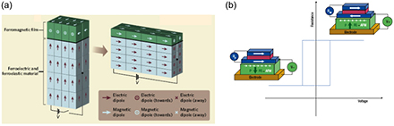
Figure 8. (a) Electrical control of ferromagnetic films. Adapted from [214], reproduced with permission (© 2008 NPG). (b) Sketch of a possible magnetoelectric random access memory (MERAM). Adapted from [215], reproduced with permission (© 2008 NPG).
Download figure:
Standard image High-resolution imageFerroelectric/multiferoic tunnel junctions
The experimental and theoretical findings suggest that FE persists in ultrathin films (~3 nm) [217], which opens up the possibility of further miniaturising devices based on FE materials. A way to exploit the FE properties of ultrathin films and the multifunctional character of MF materials is to design tunnel junctions (TJ) integrating FE or MF films as the tunnel barrier or making the TJ itself a multiferroic heterostructure [218]. At present, TJ using an insulating (nonpolar) barrier is the basis of MRAMs [219]. The FE and MF heterostructures mentioned above may take advantage of tunnel magnetoresistance (TMR) and tunnel electroresistance (TER) effects to obtain a valuable room temperature four-resistance-state-based material. It will have a broader impact due to the potential applications of TJ for the fabrication of devices. Recent theoretical and experimental studies have demonstrated the existence of TMR and TER properties in TJ, using a polar barrier (ferroelectric/multiferroic tunnel junctions (FTJ/MFTJ)) [220]. Several studies have been performed using a multiferroic as the barrier material. Gajek et al [221, 222] fabricated LSMO/La0.1Bi0.9MnO3 (LBMO) (2 nm)/Au hetero-junctions. (LBMO is a well known multiferroic at low temperature) and found the signature of four resistive states with tunnel magnetoresistance curves at 4 K at Vdc = 10 mV, after applying a voltage of ±2 V. However, this result was obtained experimentally at very low temperature (<10 K), and is not suitable for device applications at room temperature (see figure 9).
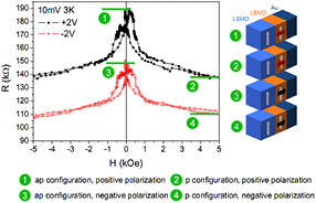
Figure 9. (a) Tunnel magnetoresistance properties of a LSMO/LBMO(2 nm)/Au junction. In the legends the meaning of ap is anti-parallel and p, parallel. Adapted from [221], reproduced with permission (© 2008 NPG).
Download figure:
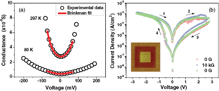
Standard image High-resolution imageRecently Katiyar's group [223] demonstrated the room temperature polar switching (see the inset in figure 10(b)) and tunneling behaviour in PbZr0.52Ti0.48O3 (PZT) ultra-thin films of thickness 3–7 nm (P3–P7), sandwiched between platinum metal and ferromagnetic La0.67Sr0.33MnO3 (LSMO) layers (Pt/PZT/LSMO). They also reported the significant enhancement in the high-resistance/low-resistance (HRS/LRS) ratio for the previously mentioned heterostructures with in-plane magnetic fields. A large variation in the high-resistance/low-resistance (HRS/LRS) ratio (2 : 1 to 100 : 1) (see figure 10(b)) was observed. The effects of the polarisation direction and poling can be seen in current density versus voltage curves and tunneling current. The conductance is fitted with Brinkman's model, and the parabolic conductance upon bias voltage implies electron tunneling governs the transport (see figure 10(a)). In this device the tunneling transmission current can be modulated by switching the PZT polarisation, thus obtaining TER with OFF/ON resistance ratio. The variety of interesting physical phenomena of these tunnel junctions and their multifunctional properties for various technological applications make the research in this field challenging and promising.
Figure 10. (a) Brinkman's model fitting of the low-resistance conductance-voltage curves for PZT- 5 nm (P5). (b) Current density versus voltage J(V) curves of the sample P7 showing the effect of applied 10 kG magnetic field. The inset shows the Piezoresponse force microscopy (PFM) measurements shows the polarisation switching images for P5 ultra-thin film. Reprinted with permission from [223]. Copyright © 2014.
Download figure:
Standard image High-resolution image
Conclusions
Over the last fifteen years, continual interest has evolved in the research of magnetoelectric multiferroic materials by the scientific community, not only in the search for new materials and structures with ME multiferroic properties with a high direct ME response, but also in the implementation of new experimental techniques that allow one to visualise changes in the magnetic response of multiferroic material due to the application of an electrical signal, and vice versa, plus the use of this response in practical applications in multifunctional devices such as sensors, transducers, memories and spintronics.
Recent experiments have demonstrated the potential applications of ME materials in prototype devices; hopefully one or more will come onto the market in the near future. The involvement of a large number of scientific groups and exponential growth in the number of publications in this area both point towards their potential functionality as materials and devices.
Acknowledgments
This work was supported by the Department of Defense (DoD) W911MF-11-1-0204, grant for release time and materials purchases. N Ortega acknowledges support from the Department of Energy (DoE)-DE-FG02-08ER46526 grant.