
Abstract
The electrical conductivity of solid-state matter is a fundamental physical property and can be precisely derived from the resistance measured via the four-point probe technique excluding contributions from parasitic contact resistances. Over time, this method has become an interdisciplinary characterization tool in materials science, semiconductor industries, geology, physics, etc, and is employed for both fundamental and application-driven research. However, the correct derivation of the conductivity is a demanding task which faces several difficulties, e.g. the homogeneity of the sample or the isotropy of the phases. In addition, these sample-specific characteristics are intimately related to technical constraints such as the probe geometry and size of the sample. In particular, the latter is of importance for nanostructures which can now be probed technically on very small length scales. On the occasion of the 100th anniversary of the four-point probe technique, introduced by Frank Wenner, in this review we revisit and discuss various correction factors which are mandatory for an accurate derivation of the resistivity from the measured resistance. Among others, sample thickness, dimensionality, anisotropy, and the relative size and geometry of the sample with respect to the contact assembly are considered. We are also able to derive the correction factors for 2D anisotropic systems on circular finite areas with variable probe spacings. All these aspects are illustrated by state-of-the-art experiments carried out using a four-tip STM/SEM system. We are aware that this review article can only cover some of the most important topics. Regarding further aspects, e.g. technical realizations, the influence of inhomogeneities or different transport regimes, etc, we refer to other review articles in this field.
Export citation and abstract BibTeX RIS

Content from this work may be used under the terms of the Creative Commons Attribution 3.0 licence. Any further distribution of this work must maintain attribution to the author(s) and the title of the work, journal citation and DOI.
1. Introduction
The specific electrical resistance or resistivity ρ of a solid represents one of the most fundamental physical properties whose values, ranging from 10−8 to 1016 Ω cm [1], are used to classify metals, semiconductors and insulators. This quantity is extremely important and is variously used for the characterization of materials as well as sophisticated device structures, since it influences the series resistance, capacitance, threshold voltage and other essential parameters of many devices, e.g. diodes, light emitting diodes (LEDs) and transistors [2].
From a fundamental point of view, the precise measurement of the resistance is closely related to other metrological units. In general, when an electric field E is applied to a material it causes an electric current. In the diffusive transport regime, the resistivity ρ of the (isotropic) material is defined by the ratio of the electric field and the current density J:

Thereby, the resistivity of the material is measured in Ω cm, the electric field in V cm−1 and the current density in A cm−2. Experimentally, a resistance R is deduced from the ratio of an applied voltage V and the current I. Only when the geometry of the set-up is well-known can the resistivity be accurately calculated, as we will show below.
As shown in figure 1(a), the resistance R is determined by measuring the voltage drop V between two electrodes, which impinge a defined current I into the sample. However, the identification of this value with the resistance of the sample is usually incorrect as it intrinsically includes the contact resistances Rc at the positions of the probes, which are in series with the resistance of the sample. This problem was encountered and solved for the first time in 1915 by Frank Wenner [3], while he was trying to measure the resistivity of the planet Earth. He first proposed an in-line four-point (4P) geometry (figure 1(b)) for minimizing contributions caused by the wiring and/or contacts, which is now referred in the geophysical community as the Wenner method [4, 5]. In 1954, almost 40 years later, Leopoldo Valdes used this idea of a 4P geometry to measure the resistivity ρ of a semiconductor wafer [6] and from 1975 this method was established throughout the microelectronics industry as a reference procedure of the American Society for Testing and for Materials Standards [7]. For the sake of completeness, the Schlumberger method will also be mentioned here. As early as 1912 he proposed an innovative approach to map the equipotential lines of soil, however, his approach relied on only two probes. Eight years later he also measured Earth's resistivity using a 4P probe configuration. In contrast to Wenner, the Schlumberger method uses non-equidistant probe spacings. The interested reader is referred to [8].

Figure 1. Schematics of (a) a two-point probe and (b) a collinear 4P probe array with equidistant contact spacing.
Download figure:
Standard image High-resolution imageTechnically, if the voltage drop V between the two inner contacts is measured while a current I is injected through the two outer contacts of the proposed in-line 4P geometry, the ratio V/I is a measure of the sample resistance R only (providing that the impedance of the voltage probes can be considered to be infinite).
Having this in mind, the question remains of how the resistivity ρ of the material can be determined from the resistance R. This review summarizes the different mutual relations between these two quantities for isotropic and anisotropic materials in various dimensions. Thereby, the description covers various geometric configurations of the voltage and current probes, e.g. collinear and squared arrangements. As we will show the 4P probe resistivity measurements are intrinsically geometry-dependent and sensitive to the probe positions and boundary conditions. The relationship between R and ρ is defined using details of the current paths inside the sample.
We will start with the recapitulation of homogeneous 3D semi-infinite bulk and infinite 2D systems which can be exactly solved. Thereafter, the effect of limited geometries is taken into account for technically relevant cases (e.g. finite circular and square samples) followed by the basics of the van der Pauw method, which can be applied to thin films of completely arbitrary shapes. Finally, we will revisit the regime of anisotropic phases based on the theoretical approaches of Wasscher and Montgomery. The careful re-analyses and applications of their methods allow us to derive for the first time the correction factors for a contact assembly inside a circular lamella hosting an anisotropic 2D metallic phase. Our theoretical conclusions will be corroborated and illustrated by the latest experiments performed using a four-tip scanning tunneling microscopy (STM) combined with a scanning electron microscopy (SEM) either in our group or by our colleagues.
We want to emphasize that this review highlights the progress made in the field of geometrical correction factors over the last century and their latest applications in low-dimensional, anisotropic and spatially confined electron gases. The inclusion of further aspects would definitely go beyond the constraints of this journal. As mentioned, this technique is used in related disciplines and readers with a geophysical background might be interested in [9, 10]. For technical aspects please see, e.g. [11–13]. Readers working in the field of surface science are referred to [14, 15], which address further aspects of semiconductor surface conductivity. At this point we would like to acknowledge the contributions from our colleagues who also work in the field of low-dimensional systems [15–17]. In comparison to the diffusive transport regime, further attention needs to be paid to probes interacting with ballistic systems, where the probes may be either invasive or non-invasive in character [18]. In this review we restrict ourselves to homogeneous phases. The conclusions, of course, change drastically if inhomogeneities are present, as mentioned in [19].
2. Four-probe methods for isotropic semi-infinite 3D bulks and infinite 2D sheets
For the ideal case of a 3D semi-infinite material with the four electrodes equally spaced and aligned along a straight line (a 4P in-line array, see figure 1(b)), the material resistivity is given by [6]

where V is the measured voltage drop between the two inner probes, I is the current flowing through the outer pair of probes and s is the probe spacing between the two probes. Equation (2.1) can be easily derived considering that the current +I, injected by first electrode in figure 1(a), spreads spherically into a homogeneous and isotropic material. Therefore, at a distance r1 from this electrode, the current density
 and the associated electric field, i.e. the negative gradient of the potential, can be expressed as

By integrating both sides of (2.2), the potential at a point P reads

For the scenario shown in figure 1(a), the voltage drop is then given by the potential difference measured between the two probes, i.e.

This concept can be easily extended to 4P geometries where the problem of contact resistances (see above) is usually avoided. According to figure 1(b), the concept presented above can be generalized and the voltage drop between the two inner probes of a 4P in-line array is

which, for the special case of an equally spaced 4P probe geometry (with s1 = s4 = s and s2 = s3 = 2s), is equivalent to (2.1).
In order to correctly calculate the resistivities from the resistances other aspects are of importance. For instance, when the thickness t of the sample is small compared to the probe spacings, i.e. for simplicity when t ≪ s (see section 3.1 for a more accurate definition), the semi-infinite 3D material appears as an infinite 2D sheet and the current can be assumed to spread cylindrically instead of spherically from the metal electrode as depicted in figure 2. The current density in this case is given by J = I/2πrt, which yields an electric field of

Repeating the same steps as for (2.3)–(2.5), a logarithmic dependency is obtained for the voltage drop between the two inner probes:

In the case of an equally spaced in-line 4P geometry the bulk resistivity is given by

i.e. the resistance is not dependent on the probe distance which directly underlines the 2D character of the specimen. In case of a homogenous and finitely thick sample the resistivity can be assumed to be constant, thus the bulk resistivity is often replaced by the so-called sheet resistance Rsh defined as

This quantity is also used to describe the spatial variation of the dopant concentration in non-homogeneously doped thick semiconductors (e.g. realized by ion implantation or diffusion). Note that the dimension of the sheet resistance is also measured in ohms, but is often denoted by Ω sq−1 (ohms per square) to make it distinguishable from the resistance itself. The origin of this peculiar unit name—ohm per square—relies on the fact that a square sheet with a sheet resistance of 1 Ω sq−1 would have an equivalent resistance, regardless of its dimensions. Indeed, the resistance of a rectangular rod of length l and cross section A = wt can be written as R = ρl/A, which immediately simplifies to R = Rsh for the special case of a square lamella with sides l = w (see figure 3).

Figure 2. Voltage V(r) and current density J(r) profiles for a semi-infinite 3D material and infinite 2D sheet.
Download figure:
Standard image High-resolution image
Figure 3. Schematic of a square 4P probe configuration with s1 = s4 = s and
 .
.
Download figure:
Standard image High-resolution imageThe four electrodes are often arranged in a square configuration rather than along a straight line. Indeed, the square arrangement has the advantage of requiring a smaller area (the maximum probe spacing is only
 against the 3s for the collinear arrangement) and reveals a slightly higher sensitivity (up to a factor of two, see below). The corresponding expression for the bulk resistivity ρ (sheet resistance Rsh) for the 4P square configuration on a semi-infinite 3D bulk is easily derived from (2.5) ((2.7) for the infinite 2D sheet) with s1 = s4 = s and
(see figure 3).
against the 3s for the collinear arrangement) and reveals a slightly higher sensitivity (up to a factor of two, see below). The corresponding expression for the bulk resistivity ρ (sheet resistance Rsh) for the 4P square configuration on a semi-infinite 3D bulk is easily derived from (2.5) ((2.7) for the infinite 2D sheet) with s1 = s4 = s and
(see figure 3).
All relations derived so far for the infinite 3D and 2D systems are summarized in table 1. From these equations it is evident that the measured resistance R does not depend on the probe spacing for the 2D case (R2D ∝ ρ·ln2 = constant), while it decreases as s−1 when increasing the probe spacing for the 3D case (R2D∝ρ/s). Naively, one would expect that the resistance should increase as the paths for the electric charges are increased, irrespective of the dimension. This counter-intuitive scenario can be rationalized by inspection of the sketches shown in figure 4 (for a linear arrangement of the probes): for an infinite 2D sheet (figure 4(a)) the expected increase of the resistance (as in the 1D case, see below), is exactly compensated by the current spreading in the direction perpendicular to the probes. In the 3D case this effect is overcompensated by the spread into the sample, which causes the s−1 probe dependence.

Figure 4. Diagrams of the current flow pattern in (a) an infinite 2D sheet and (b) a semi-infinite 3D material.
Download figure:
Standard image High-resolution imageTable 1. Bulk resistivity ρ or sheet resistance Rsh for the case of linear and square arrangements of four probes on a semi-infinite 3D material, infinite 2D sheet and 1D wire.
| Sample shape | 4P in-line | 4P square |
|---|---|---|
| 3D bulka |
 |
 |
| 2D sheetb |
 |
 |
| 1D wirea |
 |
— |
aBulk resistivity ρ. bSheet resistance Rsh, ∑ = πa2 wire section.
In contrast, a linear increase of the resistance with increasing probe distance is found only for the 1D case, where the current density is constant and independent of the distance s from the electrodes that impinge the electric current. Hence, for a circular wire with radius a, much smaller than the probe spacing (i.e. for a ≪ s), the wire appears as quasi-1D and the current density simply reads J = I/πa2. From (1.1), it is easy to see that the resistance is now proportional to the probe spacing and equals R1D = ρs/πa2 (cf table 1). Note that the conclusions drawn so far are valid both on the macroscopic as well as the microscopic scales.
As an example of a 1D system, figure 5(a) shows the corrected two-probe resistance R × ΣAve versus the probe spacing s of a semiconductor GaAs nanowire (NW) [20, 21]. The transport measurements are carried out using a multi-probe STM system (figure 5(b)) by placing, with nanometric precision, two tungsten tips on a freestanding NW (i.e. vertically oriented with respect to the GaAs substrate). The NW is 4 µm long, while its radius a decreases from 60 to 30 nm moving from the NW pedestal to the top and is at least 10 times smaller than the probe spacing (i.e. a ≪ s). We point out that the resistance of the GaAs NW is orders of magnitude larger than the contact resistances in the present case and that a two-probe configuration is in our case sufficient to infer the inherent resistivity of the NW. Examples of four-probe measurements on 1D structures can be found in [22–25].

Figure 5. (a) Two-probe resistance—corrected for the average wire section ΣAve—versus probe spacing s of a free-standing GaAs NW. The solid red line is the linear best fit of the experimental data and shows the expected s dependence for a quasi-1D system. The inset in (a) is a false-color SEM image (60 000× magnification, 45°-tilt view) of a freestanding GaAs NW with two STM tips positioned on its lateral facet [20]. (b) A photograph of a multi-probe STM system mounted in the focus of an SEM for the navigation and placement of the tungsten tips.
Download figure:
Standard image High-resolution imageFurthermore, in order to illustrate the 2D/3D transition due to the finite thickness of the sample, figure 6 shows the resistance measured on an n-type Si(1 1 1) wafer (nominal resistivity of 5–15 Ω cm, 4 × 15 × 0.4 mm3 in size) as a function of the probe spacing s [26]. The experimental data points were recorded again using a similar nano-4P STM and follow a s−1 dependence, expected for a semi-infinite 3D semiconductor, as long as the probe spacing s is within 10–60 µm, i.e. small compared to the sample thickness. The resistivity is around 7 Ω cm in accordance with (2.1) [26]. In contrast, for larger probe spacings, the current penetrates deeper into the crystal reaching the bottom and edges of the wafer. The current pattern becomes compressed and the resistance increases.

Figure 6. Electrical resistance of a Si(1 1 1) wafer crystal measured using a nano-4P STM as a function of the probe spacing. The two diagrams display the current flow pattern inside the Si(1 1 1) wafer for different probe spacings. The solid line shows the expected s−1 dependence for a semi-infinite 3D material, while the dashed curve is just a guide for the eye. Only experimental data associated with the bulk states (i.e. for probe-spacings larger than 10 µm) are reproduced from [26]. Electrical transport measurements using a smaller probe spacing are dominated by semiconductor surface states and are intentionally not reported here.
Download figure:
Standard image High-resolution imageConventional macroscopic 4P set-ups for wafer testing typically reveal probe distances in the millimeter range, which are comparable to the overall specimen dimensions [27]. The effect of confinement for the current paths is not covered by the equations derived so far. The following sections will introduce stepwise the so-called correction factors for thin/thick films which are necessary to precisely reveal the resistivities of both isotropic and anisotropic materials in various length scales.
3. Correction factors for finite isotropic samples
Real specimens are not infinite in either the lateral or vertical directions and the equations in table 1 need to be corrected for finite geometries. Equivalently, correction factors also become necessary if the probes are placed close to the boundary of a sample, as in the case of truly nano-scaled objects, and/or the probe spacing itself is comparable to the size of the samples. In such cases of finite and arbitrarily shaped samples the bulk resistivity is generically expressed as

where F = F1 · F2 · F3 is a geometric correction factor, which is usually divided into three different factors taking into account the finite thickness of the sample (F1), the alignment of the probes in the proximity of a sample edge (F2) and the finite lateral width of the sample (F3). Formally, F is dimensionally equivalent to a length, however, the correction factors F1, F2 and F3 are defined as dimensionless (see below). Further correction factors related to the cases of anisotropic and finite materials will be introduced and discussed in section 5.
The evaluation of the correction factors F1, F2 and F3 has triggered many studies. Several mathematical approaches have been used over a time span of almost 40 years, such as the method of images [6, 28–30], conformal mapping theory [31–33], solving Laplace's equations [34, 35], the expansion of the Euler–Maclaurin series [36] and the finite element method (FEM) [37], to accurately determine the values of Fi=1,2,3 for different geometric configurations and probe arrangements.
3.1. Samples of finite thickness: the correction factor F1
The resistivity of an infinite sheet of finite thickness t can be formally expressed as

where
 is the sheet resistance of an infinite 2D sheet (measured using the in-line geometry). F1 is now a dimensionless function of the normalized sample thickness (t/s) which reduces to 1 as t approaches zero (at the moment we assume that F2 = F3 = 1). A detailed derivation of the thickness correction factor F1(t/s) was given for the first time by Valdes in 1958 [6] using the method of images. This method is the first derived and to date is still the most frequently used for the calculation of the correction factors F. The factor F2 is also explicitly evaluated through this method as we will show below. However, this method results in a power series expression for F1 so it is not really suitable for numerical computation. Instead, the expression found by Albers and Berkowitz in 1985 [35] through an approximated solution of Laplace's equation will be reported here. For the case of a 4P in-line array on an infinite sheet of thickness t (electrically decoupled from a substrate), the correction factor F1(t/s) can be written as [35]

A quite similar dependence is obtained for the case of a 4P square configuration [34]. The only experimental verification of the latter formula obtained so far was by Kopanski et al in 1990 [38]. In 2001, Weller [36] re-calculated F1 through an expansion of the Euler–Maclaurin series, confirming the validity of the (3.3).
Figure 7 shows a plot of the correction factor F1 and nicely demonstrates that for t/s ≫ 1 the curves follows F1(t/s) ≈ 2 ln2(s/t), thus (3.2) reduces to the expression for a semi-infinite 3D specimen. On the other hand, for thin samples, i.e. for t/s ≪ 1, the term sinh (t/s) of (3.3) can be approximated by t/s. F1 becomes unity and (3.2) reduces to the expression of an infinite 2D sheet (see section 2, table 1). This approximation holds until t/s < 1/5 (with an approximation error around  ≈ 1%), which means that real semiconductors with a finite thickness t can be considered to be thin and approximated by a quasi-2D sheet until this condition is satisfied. Similarly, the sample can be considered of infinite thickness if t/s > 4( ≈ 1%).

Figure 7. The solid curve in the figure is the correction factor F1 versus normalized sample thickness (t/s), where t is the wafer thickness and s is the probe spacing. The dashed lines represent the two limit cases, i.e. F1 = 1 for t/s < 1/5 and F1 = 2ln2(s/t) for t/s > 4.
Download figure:
Standard image High-resolution image3.2. Probes in the proximity of a single sample edge: the correction factor F2
The correction factor F2 accounts for the positioning of the probes in the proximity of an edge on a semi-infinite sample. Albeit this idealized configuration can be realized only approximately, the equally spaced 4P in-line configuration with a distance d from a non-conducting boundary, as sketched in figure 8(a), serves nicely as a reference model to illustrate the concept of image probes, which is used extensively in the following section. The non-conducting (reflecting) boundary is mathematically modeled by inserting two current image sources of the same sign at a distance −d for current probe 4 and–(d + 3s) for probe 1, respectively [6]. Because of this mathematical trick, (2.3) still holds for a semi-infinite 3D specimen and the potential at probe 2 is given by

A similar equation is obtained for the potential at probe 3, so the total voltage drop V = V2 −V3 between the two inner probes reads

and the bulk resistivity can be written as
 with
with

The case of a 4P in-line geometry oriented parallel to a non-conducting boundary is solved in the same way. More details can be found in Valdes' original paper [6].

Figure 8. (a) Diagram of a 4P in-line array perpendicular to a distance d from a non-conducting boundary of a semi-infinite 3D specimen. Probes 1 to 4 are real while the tips 5 and 6 are imaginary and are introduced to mimic the presence of the non-conducting edge mathematically. (b) Correction factor F2 versus normalized distance d/s from the boundary (d = edge distance). The solid (dashed) curve refers to the case of four probes perpendicular (parallel) to the sample edge.
Download figure:
Standard image High-resolution imageThe dimensionless correction factor F2(d/s) for both geometric configurations (i.e. perpendicular and parallel to a non-conducting boundary) are plotted in figure 8(b). It is evident that as long as the probe distance from the wafer boundary is at least four times the probe spacing, the correction factor F2 reduces to unity (with an error of around ≈ 1%). This also explains why the data points in figure 6 follow the tendency for a semi-infinite 3D semiconductor when the probe spacing s is in the 10–100 µm range.
For instance, if the 4P array is centered on the Si wafer, which is 4 × 15 × 0.4 mm3 in size, the probe distance from the closest sample edge is about thirty times the probe spacing and F2 ≈ 1 for each of the four edges, while the thickness t remains at four or more times the probe spacing, then F1 ≈ 2s ln2/t. The resistivity equation (3.1) thus clearly reduces to that for a semi-infinite 3D sample.
It is worth noting that the correction factor F2 reaches its minimum (F2)min = 1/2 when the 4P array is aligned parallel along the sample edge. This means that the measured resistance R can increase up to a factor of two compared to the case of a semi-infinite 3D sample by moving the 4P array from a faraway location towards the sample edge. Qualitatively, this behavior can be easily rationalized since the current paths are restricted to one half of the semi-infinite 3D sample.
3.3. Samples of finite lateral dimension: the correction factor F3
The condition for F1 to be unity (t/s < 1/5) is easily fulfilled in a macroscopic 4P set-up with probe spacings in the millimeter–centimeter range [27] on wafers with typical thicknesses of 200–300 µm. Furthermore, the case of 4P probes positioned close to a single edge of the sample is also an idealized approximation and the correction factor F2 is not sufficient for a realistic description. Therefore, a further correction factor F3 is needed, which takes into account the entire effect caused by all lateral boundaries of the sample.
In this section the correction factor F3 will be discussed for two special geometric configurations which are, however, representative for a variety of practical situations, i.e. an in-line or square 4P probe geometry inside a finite circular slice (section 3.3.1) and a square 4P probe array inside a finite square (section 3.3.2). These configurations are usually used for semiconductor wafer or integrated circuit characterizations where the test windows are usually squares or rectangles.
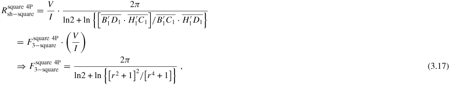
3.3.1. In-line and square 4P probe geometries inside a finite circular slice.
In 1958, Smith [29] first calculated the correction factor F3 for an in-line 4P probe array placed in the center of a circular sample using the concept of current image sources. Albert and Combs [39], and independently Swartzendruber [40], obtained in 1964 the same result by applying the conformal mapping theory [41] and transforming the circular sheet into an infinite half plane (see section 2). Here, we report the more general solution proposed by Vaughan [42], which is also valid for a squared 4P configuration and displacement of the 4P probes away from the sample center. The model is based on the following assumptions: (i) the resistivity of the material is constant and uniform (an isotropic material), (ii) the diameter of the contacts should be small compared to the probe distance (point contacts), (iii) the 4P probes are arranged in a linear (equally spaced) or square configuration and (iv) the sample thickness is much smaller than the probe spacing (t/s < 1/5: F1 = 1) and thus equivalent to a quasi-2D scenario.
Likewise, the mathematical approach used by Vaughan is based on the method of images: the resistivity formula for an infinite 2D sheet is thus extended to the case of a finite circular quasi-2D sample by introducing an appropriately located current image dipole for describing the effect of a finite boundary. This concept finally adds an additional term to (2.7) (with s1 = s4 = s and s2 = s3 = 2s for an in-line array) yielding the following voltage drop between the inner probes (V2 = H, V3 = G) for the situation shown in figure 9(a):

Now, for a 4P probe in-line geometry with an inter-probe spacing of 2s' (= s) on a circle of diameter d, where the the mid-point of the 4P geometry (E, H, G, F) is displaced at a distance αs'(βs') in the x−(y−) direction with respect to the circle center (see figure 9(a) for reference), (3.7) can be written as [42]

where the term Lα,β is a function of the position of the 4P probes
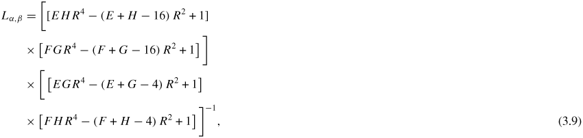
with E(F) equal to [3 + (−)α]2 + β2, G(H) equal to [1 + (−)α]2 + β2 and R = s/d.

Figure 9. Schematics of a (a) 4P probe in-line and (b) square array on a finite circular slice. The current sources outside the circle, namely E'F' in (a) and H'B' in (b), represent two additional image dipoles introduced for describing the effect of the finite boundary.
Download figure:
Standard image High-resolution imageFurthermore, when the linear probe array is centered with respect to the circular sample (i.e. α = β = 0), (3.9) is greatly simplified yielding the same result for the correction factor
 found by Smith [29]:

Figure 10(a) shows a plot of the latter equation and clearly reveals that, for d/s > 25,
 (approximation error ≈ 1%) thus, as expected, the sheet resistance
 reduces to the expression of (2.8) for an in-line array of four probes inside an infinite 2D sheet. As a rule of thumb, a finite sample can be considered as infinite when the overall width is at least one order of magnitude larger than the half probe spacing. For instance, for a 4 inch wafer, the maximum probe spacing should not exceed 5 mm. It is worth noting that
reaches a minimum value of
reduces to the expression of (2.8) for an in-line array of four probes inside an infinite 2D sheet. As a rule of thumb, a finite sample can be considered as infinite when the overall width is at least one order of magnitude larger than the half probe spacing. For instance, for a 4 inch wafer, the maximum probe spacing should not exceed 5 mm. It is worth noting that
reaches a minimum value of
 (like F2) when the external current probes lie on the sample circumference (d = 3s). In other words, the measured resistance increases by a factor of two by increasing the probe distance and moving the 4P array from the center (d ≫ s) to the sample periphery (d = 3s). For d < 3s, the correction factor
 does not have a physical meaning.

Figure 10. Correction factor F3−circle versus normalized wafer diameter d/s for (a) an in -line and (b) a square 4P probe array on a finite circular slice (s is the probe spacing for the in-line configuration and the square edge for the square configuration, respectively).
Download figure:
Standard image High-resolution imageThe case of a 4P square geometry, as shown in figure 9(b), can be solved in an analogous way [42]. Again, a current image dipole is introduced to maintain the necessary boundary conditions and an additional term appears in (2.7) (where s1 = s4 = s and
):

Vaughan [42] has shown that the latter formula can be still written in the following form:

where the parameter Sα,β is again a non-trivial function of the square 4P array displacement (αs', βs') with respect to the circle center. Further details can be found in Vaughan's original paper [42]. Here, we restrict ourselves to the case of a 4P square array placed in the center of the circle (i.e. α = β = 0), so that the correction factor
 reduces to

The correction factor is plotted in figure 10(b) as a function of d/s. As is obvious,
 for d/s > 25 (approximation error ≈ 1%) and the sheet resistance converges, as expected, to the expression for an infinite 2D sheet (see table 1). On the other hand, when the 4P probes are located on the edge of the circular sample for
 ,
,
 and the sheet resistance is

This equation refers to the case of 4P probes lying on the circumference of a circular sample and remains valid for an arbitrarily shaped sample provided with a symmetry plane. We will show this explicitly by introducing the van der Pauw theorem in section 4. Moreover, since the sheet resistance represents an intrinsic material property, both expressions (3.10) and (3.13) for
 and
and
 reveal that the current densities are increased when the 4P probe array is placed inside a finite sample (where F3⩽1), yielding to a larger voltage drop V and thus to a larger resistance. Naturally, this would result in an apparently increased sheet resistance (up to a factor of two), if we were to simply apply the formula of table 1. Finally, although formally equal to (2.8), (3.14) should not be confused with that for an in-line arrangement of 4P probes on an infinite sheet.
The method of images can be also applied to the case of a rectangular 4P array inside a circle. Interested readers are referred to appendix  for a rectangular 4P array placed in the center of a circular lamella is explicitly derived, further generalizing the results of Vaughan's theory [42].
3.3.2. A square 4P probe array inside a finite square slice.
The case of a square 4P probe array inside a finite square sample is mathematically a non-trivial scenario. In 1960, Keywell and Dorosheski [28] first determined the correction factor F3 by using the method of images. The authors correctly introduced an infinite series of current image sources to model the boundaries of the square. However, the result suffers from convergence problems, which were finally overcome by Buehler and Thurber [30] in 1977 by solving the problem in the complex plane.
Here, we concentrate on an alternative approach for calculating F3 on a square sample, which was proposed by Mircea in 1964 [31] and relies on the so-called conformal mapping theory. Interested readers are referred to [41, 43] for a detailed description of this theory. In brief, the method is based on a conformal transformation that merely maps a square specimen onto a circular geometry for which the problem has already been solved [31].
According to the conformal mapping theory, each point B(x, y) of a square can be mapped uniquely to a point B1(r, θ) of a circle as illustrated in figure 11. Consequently, if H, B, C, D are the 4P probes placed on a square lamella, we can determine four corresponding points H1, B1, C1, D1 on a circular lamella. For this scenario of four probes on a circle, a formula equivalent to (3.11) can be written and the voltage drop between V2 (= D1) and V3 (= C1) reads

where
 correspond to s2, s3, s1, s4, respectively, and H'1, B'1 is the current image dipole. At this stage it should be evident that the last equation remains valid also for the original square sample, since points H1, B1, C1, D1 correspond by definition to H, B, C, D and the problem reduces to finding a transformation between the B(x, y) and B1(r, θ) planes.

Figure 11. Schematic of a 4P square array centered with respect to a square lamella (a) and conformally mapped onto a circular lamella (b). The points H1, B1, C1, D1 in the circle correspond to the contact points H, B, D, C of the 4P square array inside the square lamella, although their position is only illustrative of the mapping procedure. H'1, B'1 is the current image dipole that needs to be introduced for describing the circular boundary. (c) Correction factor
 for a 4P square array on a finite square lamella as a function of s/d ratio and φ tilt angle. Here, s and d are the side lengths of the square 4P array and lamella, respectively.
Download figure:
Standard image High-resolution imageMircea [31] has shown that the transformation between the coordinates can be approximated by the following expressions:


where
 ,
,
 and d is now the side length of the squared lamella.
Now, if the 4P probes form a square array, which is centered with respect to the square sample (as depicted in figure 11(a)), these points are mapped for symmetry reasons again on a square array which is still centered on the circular specimen and (3.16a) and (3.16b) are greatly simplified yielding a correction factor
[31]
where r is given by (3.16a). Except for the constant factor 2π/ln2, which is now included in the definition of the term
, the last expression looks very similar to that obtained for a circle
. When inserting (3.16a) into (3.17), the correction factor is finally a function of both the normalized side s/d and the tilt angle φ of the 4P square array. The factor has been calculated and plotted in figure 11(c). As is obvious, F3 changes only by around 5% when rotating the square array φ of 45°. Likewise, in the case of the 4P square array inside a circle, moving the four probes from the sample center to the square periphery or equivalently decreasing the sample sizes from infinite (for d ≫ s) to fit the dimensions of the 4P square array (for d = s), the measured resistance increases again by factor of two.
Indeed, this effect is compensated by
when changing from 2π/ln2 for d ≫ s to π/ln2 for d = s. For the latter case we obtain for the sheet resistance
 the same expression which was obtained above for the circle (see (3.14)) and which is expected for a thin sample of arbitrary shape provided with a symmetry plane [44, 45] (see section 4):

In 1992, Sun et al [46] independently obtained similar correction factors by mapping a squared sample onto a semi-infinite half plane. They also carried out the first experimental measurements (on a 25 × 25 mm2 silicon substrate) to check their theoretical calculations. Moreover, the correction factor F3 for a square sample with a square 4P probe was evaluated numerically [37, 47, 48] using the flexible FEM.
Figure 12 summarizes the theoretical results obtained by these authors thus far using different methods (i.e. method of images, conformal mapping theory and FEM) and compares them with the experimental results of Sun et al [46]. Extremely good agreement between theory and experiment is evident.

Figure 12. Correction factor
for a square 4P probe array on a thin square sample as a function of the s/d ratio (with φ fixed at 45°). The dashed and solid curves represent the theoretical curves obtained by Mircea [31] and Sun [46] using the conformal mapping theory, while the dotted and dash-dotted curves are the theoretical results obtained by Green [47] and Shi [37] using the FEM. The open squares are the experimental values measured by Sun [46] on a 25 × 25 mm2 silicon substrate.
Download figure:
Standard image High-resolution imageThe conformal mapping theory and FEM can be also extended to the case of rectangular samples. However, the calculations become even more complicated. For details the reader is referred to [47, 49, 50].
4. The van der Pauw theorem for isotropic thin films of arbitrary shape
Of great importance for resistivity measurements is the van der Pauw theorem [44, 45], which virtually extends the formulas for evaluating the correction factor F3 for the special case of square/circular samples to a specimen of arbitrary shape, as long as the four probes are located on the sample's periphery and are small compared to the sample size. Moreover, the van der Pauw theorem requires samples which are homogeneous, thin (i.e. t/s < 1/5: F1 = 1), isotropic and singly connected, i.e. the sample is not allowed to have isolated holes.
If IAB is the current flowing between contacts A and B, while VCD is the voltage drop between contacts C and D, the resistance is given by RAB, CD = VCD/IAB (cf figure 13(a)). Analogously, we define RBC, DA = VDA/IBC. van der Pauw has shown that these resistances satisfy the following condition (ρ is the resistivity):

For samples provided with a plane of symmetry (where A, C are on the line of symmetry while B, D are placed symmetrically with respect to this line, see figure 13(b)), we immediately obtain by using the so-called reciprocity theorem RAB, CD = RBC, DA = R and (4.1) reads

This equation coincides exactly with (3.14) and (3.18) obtained in the previous section for the special cases of circular and square samples, respectively, (with the four probes located on the periphery). In the case of symmetrized samples, i.e. RAB, CD = RBC, DA, a single resistance measurement is sufficient to evaluate the sample's resistivity. For non-symmetric samples, the resistivity is generally expressed as [44, 45]

where f is now a function of the RAB, CD/RBC, DA ratio and satisfies the relation

Summarizing, (4.3) allows the determination of ρ for an arbitrarily shaped thin sample from two simple resistance measurements. van der Pauw has explicitly calculated the result of (4.3) in two famous articles [44, 45] and interested readers are referred to these for further details. In brief, the proof of the theorem consists of two parts. First, (4.3) is derived for the special case of a semi-infinite half sheet, with four probes located at the edge. Its demonstration is given explicitly in appendix

Figure 13. (a) Typical van der Pauw arrangement of the 4P probes placed along the periphery of a thin and arbitrarily shaped sample. (b) Schematics of a thin sample provided with a line of symmetry. (c) An alternative van der Pauw arrangement with the 4P probes placed along a symmetry line of the sample. See the text for details.
Download figure:
Standard image High-resolution imageIt is worth mentioning a recent revision of the van der Pauw method for samples with one or more planes of symmetry as elaborated by Thorsteinsson et al [51]. In this case, (4.1) still holds (with the exception of a factor of two, see below) if the four probes are placed along one of the planes of symmetry. The current density component normal to the mirror plane is zero, i.e. J · n = 0, for a linear 4P arrangement as shown in figure 13(c) and the potential remains unchanged by replacing the mirror plane by an insulating boundary. Consequently, the resistances are lowered exactly by a factor of two compared to the situation where the probes are positioned on the boundary. For this special scenario, depicted in figure 13(c), (4.1) can be rewritten as

As an example, if we consider the case of an in-line 4P probe array aligned along the diameter of a finite circular slice (see figure 10(a)), the evaluation of the correction factor
 (3.10) is no longer required and, according (4.5), the resistivity can be precisely extracted from two independent 4P configurations. Moreover, this geometry is robust to probe positioning errors. Note, this aspect is of importance but has not been addressed so far in the derivation of correction factor F3 (see section 3). For details see the original work of Thorsteinsson et al [51], where the error due to small probe misalignments in circular and square specimens is evaluated.
5. The 4P probe technique on anisotropic crystals and surfaces
Until the end of the 1980s only little attention was paid to anisotropic materials, the transport properties of which were seldom studied and measured. However, the growing interest in these classes of solids, which revealed pronounced electronic correlation effects (such as high-temperature superconductors [52] and low-dimensional organic and metallic conductors [53–55] also renewed the interest in their transport measurements. Moreover, also application-driven research has sustainably triggered the techniques of anisotropic conductivity measurement, e.g. the industrial application of anisotropic textiles inside high-tech woven [56, 57] or highly oriented paper-like carbon nanotubes (so-called buckypapers), carbon fiber papers inside fuel cells [58], supercapacitor electrodes [59] and even artificial muscles [60].
The evaluation of the electrical resistivity in the case of an anisotropic solid is in general more complex and demanding. For instance, the resistivity ρ is no longer a scalar, but instead needs to be substituted by a symmetric second-rank tensor, whose components ρij represent the resistivities along different directions of the solid; thus, Ohm's law (1.1) can be rewritten as
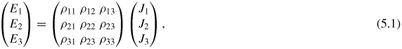
where Ei and Ji are the electric field and the density current along the ith direction, respectively. Crystallographic symmetries fortunately further reduce the number of the resistivity componentsρij. For example, two quantities ρx = ρy and ρz are sufficient for the complete description of trigonal, tetragonal and hexagonal systems while three, four and six quantities are necessary for orthorhombic, monoclinic and triclinic crystals, respectively [61, 62].
As seen, for isotropic materials the I/V ratio measured with 4P probes along one axis is directly proportional to the material resistivity if appropriate correction factors are included (cf section 3). This linear relationship fails for anisotropic materials where the I/V ratio measured along one arbitrary axis simultaneously depends on other resistivity components (e.g. ρx, ρy, ρz for orthorhombic crystals).
The main question here is how to disentangle the different components in order to fully determine the resistivity tensor. So far, this problem has been solved for crystals with a maximum of three components [63]. In this section we follow the same scheme presented in the context of isotropic crystals, i.e. we first consider the case of a 3D semi-infinite half plane and, thereafter, an infinite 2D sheet.
Finally, we will extend our focus to finite and anisotropic samples with dimensions that are comparable to typical probe distances. We first recapitulate two of the most important and relevant methods, proposed by Wasscher [32] and Montgomery [63], respectively. In this section we also derive the correction factor for a square 4P array inside an anisotropic 2D system with variable probe spacings. The theoretical results are underlined by the latest experiments on finite and 2D anisotropic systems carried out using a four-tip STM/SEM system.
5.1. Formulas for anisotropic semi-infinite 3D bulk and infinite 2D sheets
In 1961 Wasscher [64] first solved the problem of decoupling and measuring the components of the resistivity tensor and extended the formulas reported in table 1 to the case of anisotropic materials. The original solution is based on an idea of van der Pauw's [65], who suggested a transformation of the coordinates (cf figure 14) of the anisotropic cube with dimension l and resistivities ρx, ρy, ρz (along the x-, y- and z-axes) onto an isotropic parallelepiped of resistivity ρ and dimensions l'i using

where
![$\rho =\sqrt[3]{\rho_{x} \cdot \rho_{y} \cdot ~\rho_{z}}$](https://content.cld.iop.org/journals/0953-8984/27/22/223201/revision1/cm512562ieqn029.gif) and i = x, y, z. It is important to emphasize that these transformations preserve voltage and current, i.e. they do not affect the resistance R [64, 65].
and i = x, y, z. It is important to emphasize that these transformations preserve voltage and current, i.e. they do not affect the resistance R [64, 65].

Figure 14. Schematic of the mapping procedure of an anisotropic cubic sample into an equivalent isotropic parallelepiped.
Download figure:
Standard image High-resolution imageWe first will start with an in-line geometry of four probes on an anisotropic semi-infinite 3D half plane. For the sake of simplicity we further assume that the resistivities ρx, ρy, ρz are directed along the x, y, z high symmetry axes of the solid. According to (5.2), the 4P probes, which will be aligned along the x-axis of the anisotropic solid with a probe distance sx, are still aligned along the x' -axis after transformation with a distance
 . As Vx and Ix are preserved, the resistivity according to (2.1) is, for isotropic samples, given by

which can be immediately rearranged giving now for the resistance Rx = Vx/Ix along the x-axis of the anisotropic sample

The resistance measured with an in-line arrangement of 4P probes along the x-axis of an anisotropic sample is thus the geometric mean of the resistivity components along the other two principal axes. The remaining cases (a 4P probe in-line array on an infinite 2D sheet and a 4P probe square array on a semi-infinite 3D plane and infinite 2D sheet) can be solved using a similar approach. Table 2 summarizes all the formulas for the four geometric configurations considered here (in-line and square geometries in 2D and 3D). The equations are derived by assuming that the 4P in-line (square) array is aligned along the x-axis (the x- and y-axes) of the anisotropic solid (further details are given in appendix
Table 2. Electrical resistances Rx = Vx/Ix for the cases of linear and square arrangements of four probes on an anisotropic semi-infinite 3D material and infinite 2D sheet.
| Sample shape | 4P in-linea | 4P squareb |
|---|---|---|
| 3D bulk |
 |
![$\dsty\frac{\sqrt {\rho_{x} \rho_{z}}}{\pi s}\left[ {1-\left( {1+\frac{\rho_{x}}{\rho_{y}}} \right)^{-1/2}} \right]$](https://content.cld.iop.org/journals/0953-8984/27/22/223201/revision1/cm512562ieqn032.gif) |
| 2D sheet |
 |
 |
aThe 4P probes are aligned along the x-axis of the anisotropic solid with a probe distance s. bThe 4P probes are arranged in a square configuration the sides of which are aligned along the x- and y-axes, respectively. Current is applied through two probes aligned along the x-axis, while the remaining probe couple measures the voltage drop. Here s is the side length of the square.
From the comparison of the formulas shown in table 2 with those for an isotropic sample (table 1), it is evident that the measured resistances still decrease when increasing the probe distance on a semi-infinite half plane, while they remain constant for the case of an infinite 2D sheet. The reason for this behavior is still due to the current spreading in the direction normal to the probe array and into the sample when the probe distance is increased (see figure 4).
In order to reveal information about the anisotropy either the current/voltage probes need to be exchanged or the 4P probe geometry needs to be rotated. For instance, rotation of the 4P probe array by 90° reveals a resistance which is now defined by Ry = Vy/Iy. The corresponding expressions similar to those of table 2 are obtained by exchanging ρx and ρy.
Finally, the anisotropy ratio Rx/Ry, which directly refers to the anisotropy of the resistivities, is easily obtained. The equations are summarized in table 3 and plotted in figure 15 as a function of the resistivity anisotropy ρx/ρy. The dependence on ρz (for 3D materials) cancels out by evaluating the resistance ratio Rx/Ry. It is evident that the square arrangement reveals a higher sensitivity compared to the linear arrangement. In the case of an infinite 2D sheet, the anisotropy cannot be determined at all with the in-line 4P geometry. In section 3.3, we showed that the impact of finite boundaries can be neglected if the sample size is larger by one order of magnitude compared to the probe spacing. This argument still holds in the case of an anisotropic sample (see section 5.4).

Figure 15. Electrical resistance ratio Rx/Ry versus the resistivity anisotropy degree ρx/ρy for the infinite 3D half plane and 2D sheet depending on the adopted 4P probe geometric configuration (square versus in-line geometry).
Download figure:
Standard image High-resolution imageTable 3. Electrical resistance ratio Rx/Ry of an anisotropic semi-infinite half plane and infinite 2D sheet measured through an in-line and square arrangement of four probes.
| Sample shape | 4P in-linea | 4P square |
|---|---|---|
| 3D bulk |
 |
 |
| 2D sheet | 1a |
 |
aThis configuration is not sensitive at all to the material anisotropy.
In general, the equations reported in table 2 can be used to fully determine the resistivity tensor of large and thick (t/s > 4, see section 3.1) 3D samples, albeit three distinct measures are necessary, at least for the most general case of an anisotropic material with three resistivity components. In order to determine all principal resistivity directions ρi=x,y,z, which are for the sake of simplicity assumed to be parallel to each of the three principal x-, y- and z-axes, first the geometric mean
 is determined by (5.4) using an in-line arrangement of 4P probes aligned along the principal x-axis, thereafter
 is determined by rotating the in-line 4P array by 90°, finally the last term
 is obtained by cutting a thin lamella (t/s < 1/5, see section 3.1) from the thick sample and repeating the first measurement.
In this context, the characterization of anisotropic 2D materials with only two components ρx, ρy is easier. If the square 4P probe geometry is aligned with respect to the principal axes of the anisotropic surface, it is sufficient to perform the measurement twice by rotating the square array by 90° or by exchanging the combination of selected current and voltage probes. In the case that the contact geometry is not aligned accurately, the equations reported in table 2 can no longer be applied and the evaluation of the data becomes tedious and extremely arduous. As an example, we consider the latter case of a 4P probe square array on an anisotropic 2D sheet and we assume that the 4P array is rotated by an arbitrary angle θ with respect to the two orthogonal resistivity components. In this case the expression relating the measured resistance and the material resistivity becomes a function of the angle θ and reads [66] (the readers are referred to appendix

The expected resistance for arbitrary orientations of the square 4P geometry and for various resistivity anisotropy parameters is plotted in figure 16(a). As mentioned previously, the anisotropy is best seen for two orthogonal contact configurations. Furthermore, it is evident that a negative resistance appears at some θ for extremely anisotropic materials, i.e. ρx/ρy > 20. This artifact is explained by a deformation of the electrostatic potential in the case of very large anisotropies. This unexpected behavior was observed for the first time by Kanagawa et al while they were studying the transport properties of atomic indium chains on Si(1 1 1) [66].

Figure 16. (a) Theoretical angle dependence of the electrical resistance R(θ) for an anisotropic infinite 2D sheet. The different dashed curves are plotted using (5.5) with various (ρx/ρy) values. (b) Measured electrical resistance R on a single domain Si(1 1 1) 4 × 1-In surface as a function of 4P square array angular position θ with respect to the indium atomic chains. Filled symbols show the experimental values obtained by Kanagawa et al [66], while empty symbols show the results obtained by our group [70]. The solid lines in the figure are the best fitting curves for the experimental data, obtained using (5.5).
Download figure:
Standard image High-resolution imageAs a general remark, highly anisotropic 2D atomic chain ensembles have recently attracted great interest because of their exotic electronic properties, such as charge-density waves [67], spin-density waves and also signatures of Luttinger liquid [68]. In this review we restrict ourselves to the In/Si(1 1 1) system which takes the role of a benchmark system as it has been comprehensively studied over last decade. A single domain Si(1 1 1) 4 × 1-In surface is obtained by depositing a monolayer of indium onto Si(1 1 1) (miscut 0.5°÷ 2°) at 350–400 °C [69]. This 2D system is highly anisotropic because the In chains are preferentially oriented along the Si atomic steps and also electrically decoupled from the Si bulk bands by a Schottky barrier [66].
Figure 16(b) shows the resistances measured via a nano 4P STM system on such a single domain Si(1 1 1) 4 × 1-In surface as a function of the angular position θ of the assembly with respect to indium chain orientation. Some of the probe configurations have been imaged using an SEM and are shown in figure 17. The probe spacing is around 40 µm and is therefore much smaller than the dimension of the sample itself (1.5 × 0.8 cm2 in size) mimicking an infinite In layer. The filled symbols of figure 16(b) represent values measured by Kanagawa et al [66], while the empty symbols represent values obtained by our group under similar experimental conditions [70]. At a low degree of anisotropy (empty symbols in figure 16(b)), the resistance changes only slightly with θ and remains positive, while at a high level of anisotropy (filled symbols in figure 16(b)), the resistance varies strongly and becomes negative at some θ in accordance with theory. The absolute values of the resistances and the degree of anisotropy for the Si(1 1 1) 4 × 1-In surface depends significantly on the substrate cleaning procedure [71], the miscut angle (single domain), the amount of deposited indium and the deposition temperature [70]. The lower anisotropy measured for our samples is most likely ascribable to the smaller miscut angle of the Si(1 1 1) substrates (namely 1° versus the 1.8° of [66]).

Figure 17. SEM micrograph (× 2000 magnification, plan-view) of four STM tungsten tips placed on a Si(1 1 1)4 × 1-In surface. The blue dashed squares show how the 4P square array of the nano multi-probe STM system is rotated by almost 180°. θ is the angle between the square side and the indium chains, which are aligned along the Si atomic steps.
Download figure:
Standard image High-resolution imageIrrespective of the further details for the different anisotropies, it is important to note that the experimental behavior is in excellent agreement with theory as shown in figure 16(a).
5.2. Classical approaches for finite anisotropic samples
As outlined in section 3, the usual way of extending the concepts elaborated for a semi-infinite 3D bulk and/or an infinite 2D sheet to the case of finite samples involves the introduction of correction factors depending on the 4P geometry/placement and sample shape. The correction factors introduced for isotropic finite samples can be related to the anisotropic case, i.e. by mapping these anisotropic samples on equivalent isotropic ones according to the Wasscher transformations [64]. However, attentive readers may have noticed that this transformation typically maps an anisotropic square sample on an isotropic rectangle or an anisotropic circular specimen on an equivalent elliptic one, respectively. Therefore, first a revision of the correction factors
 (3.17) or
 (3.13) is mandatory before we extend this concept towards anisotropic circular or square samples (see also section 5.4).
In fact to date, the resistivity of finite and anisotropic materials is exclusively calculated via the methods introduced by Montgomery [63] and by Wasscher [32], which will be explained hereafter. In order to allow an easy analytical treatment of the problem both methods rely on some simplifications, e.g. (i) the sample has the shape of a parallelepiped [63] (or of a thin circular lamella [32]), (ii) the components of resistivity are aligned w.r.t. the edges of the parallelepiped (or along two orthogonal diameters of a circular lamella) and (iii) the 4P probes must be placed at the corners of one rectangular face (or at the boarders of two perpendicular diameters of the circular lamella). Hence, for the sake of simplicity, both these methods do not evaluate the correction factors for any arbitrary value of the probe spacing s over sample dimension d ratio (i.e. s/d), but only with probes located on the sample periphery, i.e. for s/d = 1. In section 3, we showed that the resistance R of isotropic 2D materials becomes larger by increasing the probe distance, i.e. by moving the 4P probe geometry from the sample center (for d ≫ s) towards the sample periphery (for d = s). A comparable effect takes place for finite anisotropic materials, which similarly offers a much higher sensitivity with respect to the infinite case and will be elucidated in detail in section 5.4.
In this section, we first will briefly introduce both theoretical concepts, i.e. the Montgomery and Wasscher methods, and we will subsequently compare these with recent experimental results obtained for anisotropic ensembles of In wires grown on Si(1 1 1) mesa structures of finite widths (section 5.3). In particular, the gradual rotation of the squared 4P probe geometry allows us to determine the conductivity components for this finite anisotropic system. In section 5.4 these concepts are further generalized for arbitrary probe spacings s for a 4P probe geometry inside an anisotropic circular lamella with diameter d. Using the latter method we introduce a complementary approach to measure independently the conductivity components for an anisotropic system.
5.2.1. The Montgomery method.
In 1970 Montgomery proposed a graphical method [63] for specifying the resistivities of anisotropic materials cut in the form of a parallelepiped with the three orthogonal edges l'1, l'2, l'3 collinear to the three resistivity directions ρi=x,y,z The Montgomery approach is the most commonly used method for determining the electrical resistivity of anisotropic materials (more than 500 citations) [72]. Here we describe the revised version developed by dos Santos et al in 2011 [73] which allows one to solve the problem analytically. Although this method can be applied to a rectangular prism of finite thickness, here we will derive the formulas for the case of a thin rectangular film with two distinct resistivity components ρ1, ρ2(= ρ3). For the more general case the readers are referred to [63, 73].
The revised Montgomery method is based on the Wasscher transformation (cf (5.2)) and the theoretical work of Logan et al [74], who showed that the resistance R1 = V1/I1 of an isotropic rectangular prism (with dimensions l1, l2, l3; cf figures 18(a) and (b)) is related to the resistivity ρ by means of two correction factors, E and H1, via

Thereby, the current I1 is applied via two contacts placed on one edge of the facet l1l2, while the voltage drop V1 is probed by the other two contacts on the opposite edge of the same facet (as depicted in figures 18(a) and (b)). As we will see below the correction factor E is comparable to the correction factor F1 (cf section 3) and accounts for the finite thickness of the isotropic sample. Furthermore, H1 is the analogue to the correction factor F3 and corrects the finite lateral dimensions. An equivalent relation can be written by exchanging the current and voltage probes with each other (i.e. ρ = EH2R2 with R2 = V2/I2).

Figure 18. (a) Schematics of the contact geometry for the Montgomery method and (b) the Wasscher mapping procedure of an isotropic parallelepiped on an anisotropic parallelepiped and vice versa.
Download figure:
Standard image High-resolution imageSince the contacts are placed on the corners of the parallelepiped (i.e. si = li=x,y,z and fixed), both E and H1 (or H2) do not depend on the s/d ratio, but they are a function of the ratios between sample dimensions l1, l2, l3. Logan et al [74] applied the method of images (see section 3.2) for the evaluation of the correction factors H1 (or H2), which reads

1/H2 is obtained by substituting l2/l1 with l1/l2. Similarly, the E factor can be expressed as

where s = [[(2l + 1)/l1]2 + (n/l3)2]1/2, 0 = 1 and n = 2 in the case of n > 0. As mentioned, the values of E and H were determined by graphical interpolation in the original paper of Montgomery. The revision by dos Santos et al [73] has revealed that both mathematical series can be greatly simplified and expressed through analytic equations. An in-depth analysis of (5.7a) has finally revealed that H1 can be approximated by

A similar expression is obtained for H2 when substituting l2/l1 by l1/l2.
Both equations (5.7a) (filled squares) and (5.8) (solid curve) are plotted in figure 19(a), which demonstrates the extremely good agreement between the exact and the approximated expressions over several orders of magnitude.

Figure 19. (a) Correction factor H versus the (l2/l1) ratio according to series (5.7a) (filled squares) and the approximated expression (5.8) (solid red curve). (b) Correction factor E/l3 as a function of normalized thickness
 . The dashed black lines represent the two limit cases, i.e. E/l3 = 1 for
 and
and
 for
for
 , while the solid red curve describes the transition regime for
 and it is approximated by (5.9).
Download figure:
Standard image High-resolution imageSimilarly, (5.7b) reduces to unity (i.e. E/l3 ≈ 1) for l3/(l1l2)1/2 < 0.2, while it can be approximated by
 for
for
 . These two cases correspond to those of a thin and a thick film, respectively. For
 , (5.7b) is described well by the following expression:

Figure 19(b) shows the correction factor E/l3 as a function of the l3/(l1l2)1/2 ratio and strictly reproduces the line-shape of correction factor F1 introduced above for isotropic samples (see figure 7 for comparison) but also confirming the formal equivalence between the two theories.
Based on these approximations, the resistivity can finally be related with the resistance: by means of Wasscher equation (5.2), the thin anisotropic rectangle with dimensions l'1, l'2 and l'3(≪l'1l'2) along the three resistivity directions ρ1, ρ2, ρ3 can always be mapped onto an isotropic parallelepiped with a resistivity
![$\rho =\sqrt[3]{\rho_{1} ~\rho_{2} \rho _{3}}$](https://content.cld.iop.org/journals/0953-8984/27/22/223201/revision1/cm512562ieqn051.gif) and dimensions
and dimensions
![$l_{i~=~1,2,3} ={l}'_{i} \sqrt[2]{\rho_{i} /\rho ~}$](https://content.cld.iop.org/journals/0953-8984/27/22/223201/revision1/cm512562ieqn052.gif) (cf figure 18(b)). As E ≈ l3 for the present case, it follows that
(cf figure 18(b)). As E ≈ l3 for the present case, it follows that

so that finally the Logan relation (5.6) can be expressed in terms of resistivity component ρ1

A similar equation is obtained for the second component ρ2 by exchanging l1(l'1) with l2(l'2). The unknown l1/l2 term in (5.11), which represents the length ratio of the equivalent isotropic rectangular prism, can still be determined via the same resistances R1 and R2 measured on the face l'1l'2 of the anisotropic thin rectangle. According to the analytical expressions derived by dos Santos et al, the R1/R2 resistance ratio can be written as

which is easily solved by using the hyperbolic relation sinh x = (ex − e−x)/2 and yields the following expression for l2/l1 length ratio [73]

In summary, the revised Montgomery method using (5.11), (5.13) and two simple resistance measurements permit one to fully and easily determine the resistivity components of a finite thin anisotropic rectangular lamella assuming that their directions are well defined and known. However, if the directions of the resistivity tensor are unknown but still orthogonally oriented, the problem can only be solved using the approach proposed by Wasscher which is described in the following.
5.2.2. The Wasscher method.
Wasscher described in his PhD thesis an alternative method for determining the electrical resistivity components of an anisotropic thin film [32]. Although his solution was proposed one year before that of Montgomery, very few works make use of his technique [72], probably because of the non-trivial mathematics required for its effective application. However, his studies in the field of resistivity measurements were of utmost importance and have allowed the first quantitative comparisons between the infinite and finite regimes of anisotropic thin films. This is particularly of importance for nanostructures (see below).
In a more general way, the Wasscher method can be considered as a special case of the van der Pauw method for anisotropic samples introduced in section 4. Wasscher uses the reversed mathematical approach and shows that an anisotropic rectangular or circular thin lamella can be always mapped on an isotropic semi-infinite sheet where the van der Pauw equations are valid. The demonstration is not trivial and uses both the coordinate transformation of (5.2) and the conformal mapping theory in the complex field: if P'', Q'', R'', S'' denote the locations of four probes on the edge of a semi-infinite sheet the resistances R1 = RPQ, RS = |VR − VS|/IPQ and R2 = RQR, SP = |VS − VP|/IQR, respectively, can be expressed as (see appendix


Let us consider again a thin (i.e. l3/(l1l2)1/2 < 0.2) anisotropic rectangular lamella of dimensions l1, l2 with its edges parallel to the resistivity directions ρ1, ρ2 and provided with probes P, Q, R, S on its four corners (see figure 20(a)). First, the anisotropic rectangular lamella will be mapped onto an equivalent isotropic rectangle by using the transformation of coordinates given by (5.2) (figure 20(b)). Second, a transformation of the coordinates, which makes use of the properties of Jacobian sine-amplitude elliptic function sn(K(k), k) in the complex field, maps the four probes P', Q', R', S' onto the upper half plane of the complex plane P'', Q'', R'', S''. At this point, it should be evident that the resistances R1 = V1/I1 and R2 = V2/I2 of the anisotropic rectangular lamella (where Ii=1,2 is the current injected via two probes along one edge and Vi=1,2 the corresponding voltage drop on the opposite edge) can be measured using (5.14a) and (5.14b), since all the transformations preserve both currents and voltages. Thus, the problem reduces to finding the general correspondence formula between the original four probes P, Q, R, S on the anisotropic rectangle and the corresponding P'', Q'', R'', S'' probes on the semi-infinite sheet. A quite similar case was already described in section 3.3.2. We will not report the details here, but instead call the attention of interested readers to the original thesis [32]. In brief, the coordinates of the original probes mapped onto the upper half sheet of the complex plane are expressed by


where K(k) is the complete elliptic integral defined as

and where sn(z, k) is the so-called sine-amplitude function defined as the inverse of the incomplete elliptic integral of first kind:

We point out that for the incomplete elliptic integral, the upper limit x becomes a function of z, called the amplitude of z. So the Jacobi sine-amplitude is the sine of the upper bound of the incomplete elliptic integral obtained by inverting the F function (i.e. x = F−1(z, k)) [75, 76]. Both equations depend on the modulus k, which is only a function of the resistivities and lengths of the anisotropic rectangular lamella and is given by the inverse of the so-called Jacobi's nome q(k):

When the Wasscher method was published, the values of the nome q(k) as well as the numerical values of elliptic integrals (5.16a) and (5.16b) as functions of k were given in mathematical tables [77], but now computer software, such as Matlab [78] or Wolfram Mathematica [79], allows their rapid and easy evaluation with high numerical precision.

Figure 20. Schematics of (a) an anisotropic rectangular sample with edges parallel to the resistivity directions, (b) the equivalent isotropic rectangular sample after Wasscher transformation and (c) the final mapping onto the upper half plane of the complex plane.
Download figure:
Standard image High-resolution imageEvaluating the distances P''Q'' := P''(1/[k sn(K, k)], 0) − Q''(−1/[k sn(K, k)], 0), etc, and replacing them into (5.14a) and (5.14b), we finally obtain


Similarly to the Montgomery method, the numerical solution of both (5.17a) and (5.17b) allows the evaluation of both resistivity components ρ1, ρ2 from two single resistance measurements (i.e. R1 and R2).
The main advantage of this mathematical approach relies on its simple generalization to the case of a circle. Indeed, if we consider now a thin anisotropic circular lamella, of radius r and thickness t(<(d/5)), with all four point probes placed on its circumference d along two orthogonal diameters, and we call φ the angle between the two orthogonal resistivity components ρ1, ρ2 and the lines intersecting the two opposite contacts as shown in figure 21(a), the corresponding resistances measured on a circle read [32]:


where now the modulus k is given by the inverse of Jacobi's nome (q(k))circle :

Figure 21(b) shows (5.18a) as a function of φ with different (ρ1/ρ2) resistivity ratios. The graph is only shifted by π/4 with respect to the infinite case of figure 16(a) which is plotted as a function of θ = 5π/4 − φ (see figure 21(a) for reference). Interestingly, contrary to the infinite case, the resistance remains always positive, even for high anisotropies.

Figure 21. (a) Schematic of an anisotropic circular lamella with the 4P probes placed on two vertical diameters and rotated by φ degree w.r.t. the resistivity directions. For the sake of clarity, we also show the angleθ = 5π/4 − φ used in figure 17 to define the angular position of the square 4P array w.r.t. the resistivity directions. (b) The calculated angle dependence of electrical resistance R(φ) for an anisotropic finite circular thin film. The solid curves are plotted using (5.18a) with different (ρ1/ρ2) resistivity ratios.
Download figure:
Standard image High-resolution imageAs in the case of an infinite sample the resistivity directions can be found easily and their values consequently determined by rotating the entire 4P array. As is obvious the (R1)circle/(R2)circle ratio takes its maximum for φ = π/4 (orθ = π/2), because R1 is maximum (see figure 21(a)), while R2, which has a similar dependence on φ but shifted by 90° with respect R1, has its minimum. Since sn(4K(k)φ/π, k) = 1 for φ = π/4, one immediately obtains from (5.18a), (5.18b)

Similarly, the resistance anisotropy as a function of resistivity anisotropy degree ρ1/ρ2 for a rectangular or square (with l1 = l2 = l) lamella with the probes located on its corners is easily derived from (5.17a), (5.17b). Both dependencies are plotted in figure 22 together with those obtained on anisotropic infinite 2D sheets (cf table 3). As is obvious, the electrical resistance ratios Rx/Ry(= R1/R2) of a finite anisotropic film can be increased by several orders of magnitude compared to an infinite film although its resistivity ratio ρx/ρy(= ρ1/ρ2) is the same. The dependency on the geometry of the sample is much weaker. Therefore, a much higher sensitivity is expected when the 4P probes are placed on the sample periphery (i.e. s = d or s = l) compared to the infinite case (i.e. s ≪ d or s ≪ l). However, care should be taken when measuring the resistivities of finite anisotropic materials. While for isotropic samples the error can be only a factor two, it can hugely increase for the case of finite anisotropic lamella structures.

Figure 22. Electrical resistance ratio Rx/Ry(= R1/R2) as a function of resistivity anisotropy degree ρx/ρy(= ρ1/ρ2) for an infinite 2D sheet and a finite circular and square lamella. The solid curves, referring to finite geometries, are plotted using (5.17a), (5.17b) (with l1 = l2 = l) and (5.20) of the Wasscher method. The filled symbols are obtained from (5.10) and (5.12) of Montgomery's method (here assuming l'1 = l'2).
Download figure:
Standard image High-resolution imageFinally, the full squares in figure 22 display the values determined using the Montgomery method (with l'1 = l'2, (5.10) and (5.12)). The perfect agreement with the solid curve, obtained using the Wasscher method relying on a completely different approach, underlines once more the robustness of both mathematical solutions.
5.3. An experimental comparison between the finite and infinite regimes for anisotropic 2D systems
We have introduced in section 5.1 the In/Si(1 1 1) system as an anisotropic 2D benchmark system to determine the resistivity tensor and will now use the same system on spatially restricted areas to prove the increase of the resistance ratio discussed in the context of figure 22. Please see section 3 for any details on the infinite (i.e. unconfined) In/Si(1 1 1) system.
The spatially restricted 4 × 1-In wire system grown on circular Si(1 1 1) mesa structures, i.e. elevated Si(1 1 1) islands, is illustrated by figure 23(c). The resistivity components have been again determined by means of a four-tip STM/SEM system.

Figure 23. (a) SEM micrograph (1000× magnification, plan-view) of circular mesa structures fabricated using optical lithography and RIE onto a Si(1 1 1) substrate. (b),(c) An SEM image and a schematic of the four tungsten tips placed with nanometric precision on the periphery of the mesa structure. (d) Electrical resistance of the 4 × 1-In system as a function of 4P array angular position R(θ) on (empty symbols) and faraway from (filled symbols) the Si mesa structure. The solid red and blue lines are the best fitting curves of the experimental data, obtained using (5.18) and (5.5) for the finite and infinite regimes, respectively.
Download figure:
Standard image High-resolution imageThe mesa structures in this case have a diameter of 30 µm and a height of 500 nm (figures 23(a) and (b)) and were fabricated using optical lithography and reactive ion etching (RIE, using SF6) onto a Si(1 1 1) semiconductor wafer (a miscut of 1° toward the [−1–12] direction and P-doped, 500–800 Ω cm). A clean Si(1 1 1) 7 × 7 surface [80, 81] is thus obtained through the vigorous chemical treatment of the sample including standard RCA-1 cleaning [82] in air and subsequent flash annealing cycles up to 900 °C under ultra-high-vacuum (UHV) conditions. The 4 × 1-In phase is finally obtained by adsorption of an indium monolayer at 400 °C.
By means of a high-resolution SEM, the four tungsten tips of the multi-probe STM are independently navigated with nanometer precision to the mesa periphery as shown in figure 23(b) and individually moved to the 4 × 1-In surface via feedback control approach mechanisms. The electrical resistance of the 4 × 1-In atomic chains is thus measured as a function of the 4P square array angular position on the circular mesa periphery. In order to compare these measurements on finite areas we performed similar measurements with the same contact geometry on the lower quasi-2D infinite areas at least 300 µm away from the circular mesa structure. In this way we can realize resistivity measurements on infinite as well as finite areas on the same sample and ensure that the average defect densities are approximately the same. Both measurements are plotted in figure 23(d) showing clearly the effect of confinement. The resistance anisotropy degree for the 4 × 1-In system grown onto the circular mesa surface (empty symbols) is around (Rx/Ry)Mesa = 17.4 compared to (Rx/Ry)2D = 3.5 measured on the large and flat area of the same sample. The solid curves reveal the best-fits of the experimental data using (5.18a) or (5.18b) and (5.5) for the finite and infinite case, respectively, for the resistivity components ρy = 6.2(±1.2) × 104Ω sq−1 and ρx = 16.7(±1.0) × 104Ω sq−1 yielding a resistivity anisotropy degree ρx/ρy ∼ 2.7
This result is of importance, because it directly confirms that a much higher sensitivity (of one order of magnitude or more) can be easily achieved when the sample size becomes comparable to the probe distance and validates both theoretical models introduced for the description of infinite and finite regimes. Furthermore, we notice that the minimum resistance (i.e. parallel to the indium chains) for our 4 × 1-In system is ∼5 × 10³Ω, one order of magnitude larger than the value reported in figure 16(b) for an indium layer deposited under similar conditions. We point out that the difference is not related to the probe spacing and sample geometry, but is most likely due to the lower annealing temperature (900 °C versus 1200 °C) in order to preserve the mesa structures. This leaves a higher concentration of surface defects behind which is responsible for the larger measured resistance [71], although the relative values (i.e. the resistivity anisotropy degree ρy/ρx) remain comparable. Nonetheless, the spatial constriction reveals the unique possibility of controlling and correlating the impact of defects in surface transport.
5.4. Correction factors for a square 4P array inside an anisotropic circular area
In order to derive the resistivity components of a finite and anisotropic material by means of the Montgomery [63] or Wasscher [32] methods, the 4P probes must be precisely positioned on the sample periphery (see section 5.2). To the best of our knowledge, the correction factor for arbitrary probe spacings s on samples with size d, i.e. F(s/d), again for the case of a finite anisotropic medium, has so far not been derived.
In the following we will explicitly calculate the correction factor for the case of a square 4P probe array placed in the center of an anisotropic circular slice with two distinct and mutually orthogonal resistivity components ρx, ρy(= ρz). As we will show further, our theoretical result is fully in line with the latest experiments performed on the 4 × 1-In wire system selectively grown on circular Si(1 1 1) mesa structures.
Figure 24(a) shows the schematics of a four-'point' probe square array placed in the center of a 'thin' anisotropic circular medium. As in the context of the Wasscher method, we still assume that both the probe size and sample thickness are small w.r.t. the probe spacing, i.e. we restrict our analysis to a quasi-2D scenario. In agreement with the nomenclature adopted throughout this review, s is the distance in between next-neighbor probes, while d is the diameter of the circle. Furthermore, for the sake of simplicity, we suppose that the square edges of the 4P probe array are parallel to the two resistivity components, ρx and ρy. At the end of this section we will generalize this to arbitrary angles of rotation (cf section 5.3).

Figure 24. (a) Schematics of a 4P probe square array placed in the center of an anisotropic circular sample. The square edges are assumed to be parallel to the resistivity directions ρx and ρy. (b) A diagram of the electrically equivalent elliptical isotropic sample and rectangular 4P array and (c) related subsequent mapping onto a unit circle.
Download figure:
Standard image High-resolution imageBy applying (5.2) (the Wasscher method), the anisotropic circle (figure 24(a)) is first transformed into an electrically equivalent isotropic ellipse of resistivity
![$\rho =\sqrt[3]{\rho_{x} \rho_{y} \rho _{z}}$](https://content.cld.iop.org/journals/0953-8984/27/22/223201/revision1/cm512562ieqn053.gif) with the semi-axes
with the semi-axes
 (and thickness
 ), while the square 4P probe assembly is simultaneously stretched into an electrically equivalent rectangular 4P probe assembly. In figure 24(b), the special case ρy/ρx = 2 is depicted. In general, the aspect ratio of the rectangle depends on the anisotropy degree of the original circle.
According to the conformal mapping theory (cf also section 5.2.2), we know that the interior of an ellipse (i.e. every point z of an ellipse) can be mapped onto a unit circle ([41], ch 6, p 296) by the function

with | w| < 1. Where z is the position of an arbitrary point inside the ellipse (expressed in complex coordinates), K(k) denotes the complete elliptic integral of modulus k (5.16a), whose value is given by the inverse of Jacobi's nome (q(k))circle (see (5.19)) and depends on the resistivity values of the original anisotropic circle. It is easy to demonstrate that the four initial points A, B, C, D shown in figure 24(a) are mapped onto the points A'' = f(A'), B'' = f(B'), C'' = f(C'), D'' = f(D') in the unit circle with the following coordinates:


These equations have been plotted in figure 24(c) (using Wolfram Mathematica). The dashed black curves show how the coordinates of the four points change as the d/s ratio is varied. It is worth noting that the 4P array still has a rectangular appearance on the unit circle, however, the paths of the corners when going from zero up to the circle diameter d (i.e. for
 ) are curved as indicated by the arrows. Furthermore, the angle between the two curved paths depends on the anisotropy degree of the original circle (see the gray dashed curves in figure 24(c) for reference).
Fortunately, the case of a rectangular 4P array placed in the center of an equivalent isotropic circular slice can be easily solved by applying the method of images, further generalizing the Vaughan solution [42] for a 4P square array (see section 3.3.1 above). If the current Iy is injected, according to figure 24(c), via the probes B'' and C'', while the voltage Vy is probed between A'' and D'', the resistance Ry for the present rectangular probe configuration inside a circle reads

where r = a/b (with
 and
and
 , see figure 24(c)) is the aspect ratio of the rectangle mapped on the unit circle and
 is the general correction factor for a rectangular 4P array placed in the center of an isotropic circular slice, which reads

For the present case d'' = 2 which is the diameter of the unit circle. For further details regarding the derivation of these equations the reader is referred to appendix  , and (D.7), respectively).
As is obvious from (5.23), the correction factor Fy(s/d), albeit formally linked to the correction factor
for a rectangular 4P array in an isotropic circle, represents (via (5.22a)–(5.22d)) the correction factor for a 4P square array placed in the center of an anisotropic circle and aligned as depicted in figure 24(c) (i.e. with the current probes parallel to the ρy component). Based on (5.22a)–(5.22d) and (5.24), this correction factor can be numerically calculated with high precision as we will show below.
In order to determine the entire resistance anisotropy ratio the orthogonal Rx component is needed. By exchanging the current and voltage probes an equation similar to (5.23) can be written for the resistance Rx parallel to the ρx component

Similarly to the former case, now a correction factor Fx(s/d) is introduced which depends on
 :
:

From the ratio of (5.25) and (5.23), we obtain a compact expression for the anisotropy ratio Rx/Ry, which directly refers to the resistivity components ρx and ρy inside the anisotropic circle and normalized circle diameter d/s and simply reads

This resistance anisotropy ratio can be numerically derived using (5.22a)–(5.22d). Figure 25(a) shows the ratio as a function of the normalized circle diameter d/s for various resisitivity anisotropy values. It is apparent that the measured electrical resistance ratio Rx/Ry rises exponentially as the squared probe assembly is moved from the center (d ≫ s) to the circle periphery
 . As expected, the values we obtain from (5.27) for the limits d ≫ s (infinite 2D sheet) and for
 (i.e. probes on the circle circumference) coincide with the values plotted in figure 22.

Figure 25. (a) Theoretical electrical resistance ratio Rx/Ry versus normalized wafer diameter d/s for a square 4P probe array placed in the center of an anisotropic circle (s is the square edge of the 4P array). The solid curves are plotted using (5.27) with different (ρx/ρy) resistivity ratios. (b) Experimental electrical resistance ratio Rx/Ry versus normalized wafer diameter d/s measured on a 4 × 1-In wire system selectively grown on a circular Si(1 1 1) mesa structure (d = 20 µm). The empty and filled symbols refer to two different mesas of the same sample. The solid line in the figure is the best fitting curve of the experimental data, obtained using (5.27).
Download figure:
Standard image High-resolution imageIn order to confirm our above considerations, we again used the 4 × 1-In reconstruction grown on a circular Si(1 1 1) mesa structure (diameter d = 20 µm) and measured precisely the resistance components parallel (Ry) and perpendicular (Rx) to various probe spacings s. The correct alignment of the probes was performed before using the rotational square 4P method discussed in the context of figure 23(d). We thereafter measured both resistance values sequentially by approaching the tips from the periphery toward the mesa center. As shown in figure 25(b), the ratio decreases exponentially from a value of Rx/Ry ∼ 11 with the tips at about 1 µm from the circular border down to a minimum value of Rx/Ry ∼ 3.5 when the probes are at a distance of only 3 µm. The solid curve is the best-fit using (5.27) and yields a resistivity anisotropy of ρx/ρy = 2.5 ± 0.1 which perfectly agrees with the values determined (independently) using the rotational square 4P method. We notice that some data points appear slightly scattered w.r.t. the fitting curve and this is most likely due to uncertainties regarding the positioning of the tips or possibly inhomogeneities within the In reconstruction on the Si(1 1 1) mesa itself.
As just seen, the probe distance dependent measurements of the resistance in a finite area can be used to correctly determine the resistivities. Finally, we would like to demonstrate that this technique can be combined with the rotational square method mentioned in sections 5.2.2 and 5.3. In this case, function (5.21) maps the 4P square array on an electrically equivalent parallelogram inside the unit circle and the new coordinates of (5.22a)–(5.22d) depend explicitly on the azimuthal orientation of the 4P assembly. Technically, the approach is similar to what we outlined in the appendix for the rectangular geometry used above. Thus we will not repeat all of the steps in detail but show the final result for the resistance R(ρx, ρy, φ, s/d) in figure 26 exemplarily for one set of resistivity components ρy = 6.2(±1.2) × 104Ω sq−1 and ρx = 16.7(±1.0) × 104Ω sq−1.

Figure 26. Theoretical calculation of the resistance for a 4P square array placed in the center of a finite anisotropic circular lamella as a function of the d/s ratio and angle of rotation θ w.r.t. the directions of anisotropy. Here, s and d denote the side length of the square 4P array and the diameter of the circular lamella, respectively. The plot is obtained by setting the resistivity values to ρy = 6.2(±1.2) × 104Ω sq−1 and ρx = 16.7(±1.0) × 104Ω sq−1. These values coincide with those obtained for the In-4 × 1 phase shown in figure 23(d).
Download figure:
Standard image High-resolution image6. Conclusions and outlook
In this review paper we have revisited the 4P probe technique with a special emphasis on the geometrical correction factors for both isotropic and anisotropic systems in order to determine the electrical resistivity from apparently simple resistance measurements. Despite its long history of almost a hundred years, the 4P probe transport technique is still a leading method in both fundamental and application-driven research. Along with the development of sophisticated multi-probe STMs, this technique can now be applied successfully even in the truly nanometer scale. Particularly for nanostructures and, in a more general sense, for spatially restricted areas, the aspects of anisotropy and the current paths need to be considered to reveal reliable values for the resistivity.
As outlined in detail in section 3, the resistance R and the resistivity ρ are generally linked by dimensionless correction factors F, which in turn depend on the probe geometry and assembly as well as the structure of the sample. Even more important, the dimensional crossover which occurs along the transition from the infinite to the finite regime, depending on ratio between the probe spacing s and sample size d, can be accurately taken into account. As seen for infinite (i.e. s/d ≪ 1) and finite scenarios (i.e. s/d = 1), the apparent resistance of isotropic materials may increase by a factor of two which, on the other hand, can also be caused by different probe geometries or sample structures. An exception is the well-known van der Pauw method, where the shape of the sample is not important as long as the four probes are located on the sample periphery or along one of its planes of symmetry; details are discussed in section 4.
On the other hand, anisotropic materials, as discussed in section 5, still remain challenging since two or three resistivity components are needed for a complete characterization. As recently as 40 years ago full analytical treatment was possible only for the special case of infinite samples (i.e. s/d ≪ 1) or finite rectangular/circular specimens with the 4P probes located on the sample periphery (i.e. s/d = 1). Although the van der Pauw theorem has been shown to be applicable to anisotropic materials of arbitrary shape as well, it only allows one to measure the geometric mean
without being able to disentangle the individual resistivity components [83, 84]. The methods introduced by Wasscher and Montgomery are routinely applied to the measurement of resistivity components in anisotropic materials, but the validation of some effects such as the negative resistance at a high degree of anisotropy [66] as well as the increase of the sensitivity of the 4P probe technique in a finite geometry set-up have only recently been demonstrated and are also the subject of this review article. In particular, the latter aspect is important as high resistance anisotropies are also induced by spatial restrictions (e.g. steps, inhomogeneities, etc) which in turn could lead to incorrect resistivity values. Only a few attempts have been made to date in the calculation of correction factors F for anisotropic materials as a function of the probe distance compared to the sample dimension d [32, 85, 86]. In the course of this review we have calculated for the first time the general case of a square 4P geometry inside a circular anisotropic system.
In this review we restrict ourselves to homogeneous phases. However, large samples in particular may exhibit various phases causing spatial variations with regard to transport properties, e.g. carrier mobilities and densities. In this case, the interpretation is not straightforward. The first studies, which date back over fifty years, have shown that 4P probe measurements are only qualitatively sensitive to non-uniformities in the case where their diameter is larger than the probe spacing and yield less information (i.e. averaging their effect) when their diameter is much smaller [40]. Therefore, 2D and 3D contour map techniques have been developed over time in order to precisely characterize the variation of wafer resistivity [87]. Only recently, this problem was encountered in theoretically providing analytical functions in order to be able to simulate the sensitivity of 4P probe measurements towards local inhomogeneities [19].
Furthermore, the effect of the finite widths of the contacts themselves needs to be taken into account in order to improve the accuracy in resistivity measurements. In this work we assumed ohmic and sufficiently small contacts, e.g. point contacts, compared to sample size. If this condition is not fulfilled, the resistivity expressions for the infinite 3D half plane and 2D sheet, further generalizing those reported in table 1, can be derived [88–90]. In the case of finite isotropic samples, van der Pauw has provided the first rough estimate of the error associated with large contacts anchored to the sample periphery, being of the order Δρ/ρ ∼ l2/d2 (where l and d are the contact width and sample size, respectively) [44, 45]. A more detailed analysis using conformal mapping theory [91–94] and numerical simulations [95, 96] was carried out for rectangular and circular samples. A method that is valid for samples of arbitrary shape and that generalizes the van der Pauw approach was first proposed recently by Cornils et al [97–99]. The impact of finite contacts for anisotropic materials has been analyzed only in part and has actually been solved for the special case of circular thin films [33].
Further efforts and development are certainly required and expected in the near future in this field, considering the increasing interest in anisotropic materials and the striking applications of 4P probe techniques.
Acknowledgments
We gratefully acknowledge the financial support of this project by the DFG through the projects FOR1700 and Te 386/9-1. Furthermore, IM wishes to acknowledge the Institut für Festkörperphysik at Leibniz Universität of Hannover for their hospitality and the 'Angelo della Riccia' Italian foundation for supporting his stay there during the period during which this review was written.
Appendix A.
The van der Pauw formula can easily be derived for the special case of a semi-infinite thin film. This trivial calculation reveals the origin of the exponential factor in (4.1) and helps in the understanding of the method proposed by Wasscher for the evaluation of resistivity components for the case of a finite thin anisotropic rectangular or circular lamella (see section 5.2.2). Taking figure A1 as a reference, we assume that the 4P probes are placed along the edge of a semi-infinite 2D sheet. The current is injected and collected through the Q and R probes respectively, while the voltage drop is measured between the probes S and P. The sample thickness is assumed to be much smaller than the probe distance, thus the current density J can be immediately expressed as J = I/πrt yielding for the voltage drop VSP

where the first term is the voltage drop due to the current injected by probe Q, while the second term is the voltage drop due to the current leaving the sample via probe R. Rearranging (A.1), we thus obtain

If we now change the current and voltage probes, we can similarly write

At this point we notice that

since

The final equation is derived by substitution of QR, RS, SP with the probe spacing s, and it demonstrates the van der Pauw formula for the special case considered here.

Figure A1. Schematic of the semi-infinite 2D sheet considered here for the special proof of the van der Pauw equation
Download figure:
Standard image High-resolution imageAppendix B.
In this appendix, the formulas presented in table 2 for infinite anisotropic solids will be calculated. The case of an in-line arrangement of four probes on an anisotropic semi-infinite 3D half plane is described in section 5.1. Here, we first consider the case of an in-line arrangement of four probes on an anisotropic infinite 2D sheet. We further assume that the resistivity components ρx, ρy, ρz are directed along the x-, y- and z-axes of the sample. If the 4P probes are aligned along the x-axis with a probe distance sx, the same probes will have a distance
on an equivalent isotropic lamella of thickness
 after applying (5.2). On this isotropic sheet, Vx and Ix are preserved while (2.8), which is still valid, yields for the singular resistivity ρ

which can be immediately rearranged yielding the following equation for the measured resistance along the x-axis of the original anisotropic sheet,

i.e. the resistance in an anisotropic 2D sheet is still the geometric mean of the resistivity components, but now lying on the same plane of the 2D lamella. Although similar, the demonstration of the two remaining equations summarized in table 2 for a square arrangement of the probes is slightly more complex. Taking as a reference the schematics of figure B1, the 4P square array placed on an anisotropic sample and aligned along the x- and y-axes is transformed into a 4P rectangular array, still aligned along the x- and y-axes of the equivalent isotropic sample of resistivity ρ and dimensions

where s1 = s4 = s is the side while
 is the diagonal of the original square array.

Figure B1. Mapping of (a) a 4P square array placed on an anisotropic sample into (b) a 4P rectangular array placed on an equivalent isotropic specimen.
Download figure:
Standard image High-resolution imageIf we now insert (B.3) into expressions (2.5) for a 3D semi-infinite half plane, which remains valid on the transformed isotropic sample, we obtain

Equation (B.4) represents the relation between the measured resistance and the resistivity components of the anisotropic sample for the case of a very large and thick 3D specimen. Inserting (B.3) into expressions (2.7), we finally obtain the resistance expression for the case of a square arrangement of four probes on an anisotropic infinite 2D sheet:

Appendix C.
The formulas for infinite anisotropic samples reported in table 2 are deduced assuming the principal resistivities ρi and the 4P probe array aligned along the xi-axes, but this condition is not always satisfied. Here we derive the more general equation (5.5) for the special case of a square probe array placed on an anisotropic infinite 2D sheet and rotated by an arbitrary angle θ with respect to one of two orthogonal resistivity components ρx, ρy. If A, B, C, D are the starting probe positions of the 4P square array on the anisotropic sample, their positions A', B', C', D' after an arbitrary rotation of θ can be easily evaluated by applying the 2D rotation matrix

which gives

Next, we map the contacts points of the rotated square array on an equivalent isotropic sample using (5.2):

As shown in figure C1(b), we now calculate the probe spacing s''1 = A''D'', s''2 = A''C'', s''3 = B''D'', s''4 = B''C'' of the rotated and transformed 4P array:


Figure C1. (a) Rotation of the 4P square array of an arbitrary angle θ with respect to the x- and y-axes and (b) successive mapping onto an equivalent isotropic sample.
Download figure:
Standard image High-resolution imageFinally, we insert (C.4) into (2.7), which remains valid on the equivalent isotropic sample where the 4P square array is mapped. After some rearrangements, we obtain

which coincides with (5.5) and describes how the measured resistance changes as a function of the 4P square array angular position θ and the resistivity anisotropy degree of the 2D infinite sheet.
Appendix D.
The derivation of the correction factor
 for a rectangular 4P array placed in the center of an isotropic circular lamella is based on the following assumptions: (i) uniform resistivity, (ii) point contacts and (iii) a sample thickness much smaller than the probe spacing (thus equivalent to a quasi-2D scenario). Hence, figure D1(a) shows a rectangular 4P array placed in the center of an isotropic circular lamella, where B and C are the current probes while A and D are the voltage probes of the 4P array, both are positioned at a distance p from the center (denoted by O). If we neglect for a moment the circular finite boundary, we can easily obtain by means of (2.7) (with s1 = s4 = b and
 the voltage drop Vy for a given current Iy, which is

where a and b are the sides of the rectangle. It is evident that (D.1) immediately converges to the expression for a 4P square array when a = b (which is strictly valid only for an infinite or unlimited 2D sheet). According to the method of images, the effect of an isolated circular finite boundary can be mathematically described by adding two current images P and Q, both placed at a distance d2/4p from the circle center O (where d is the circle radius) and along two straight lines connecting the circle center with the two current probes C and B (see figure D1(a)). It is easy to verify that the adopted configuration of real and image currents compensates the electrostatic potential along the circumference of the circular lamella [100] and allows one to correctly evaluate the potential inside the circle. For this scenario of four current probes, the voltage drop between V2(= D) and V1(= A) now reads


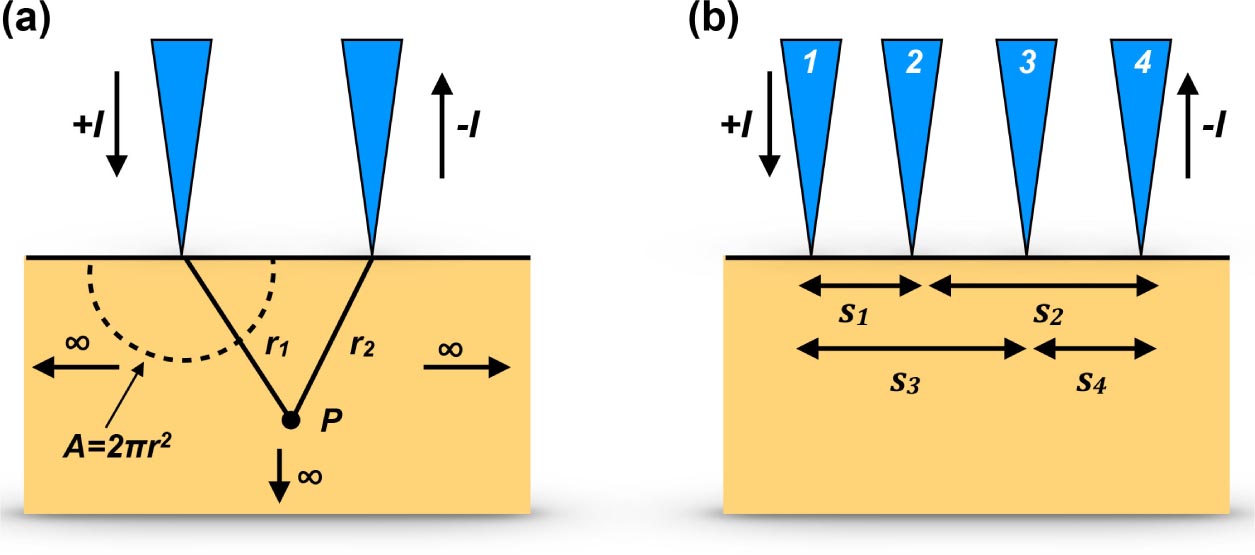
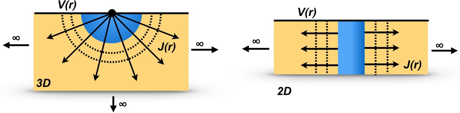
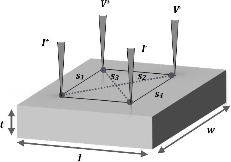
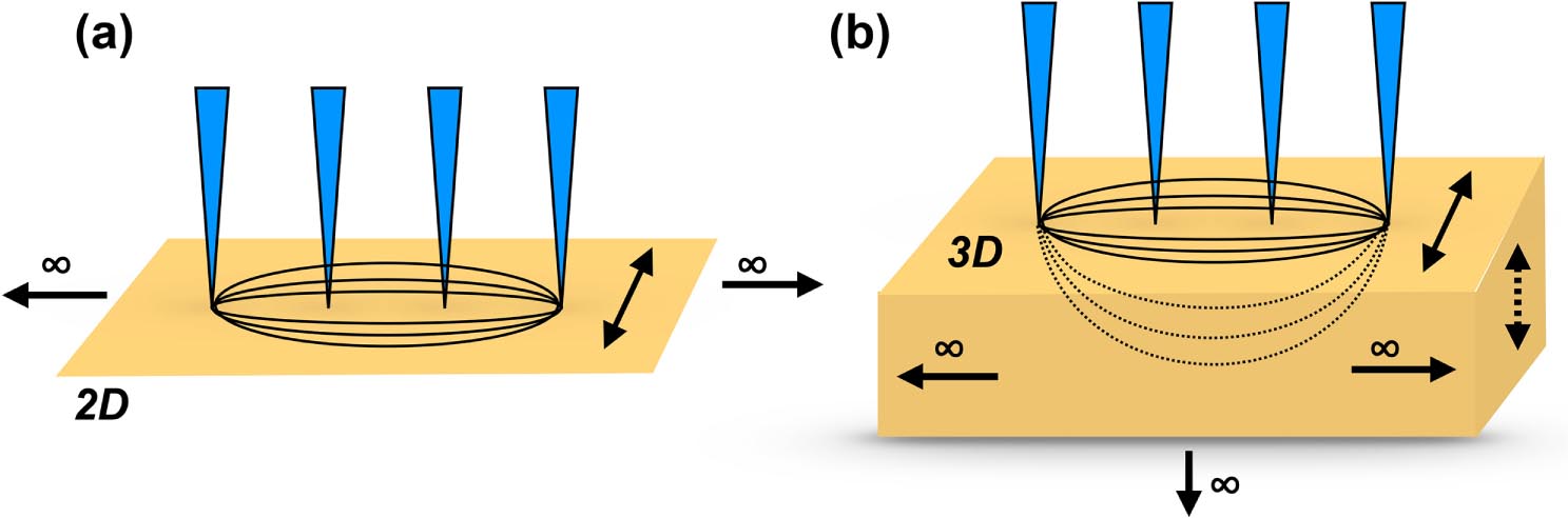
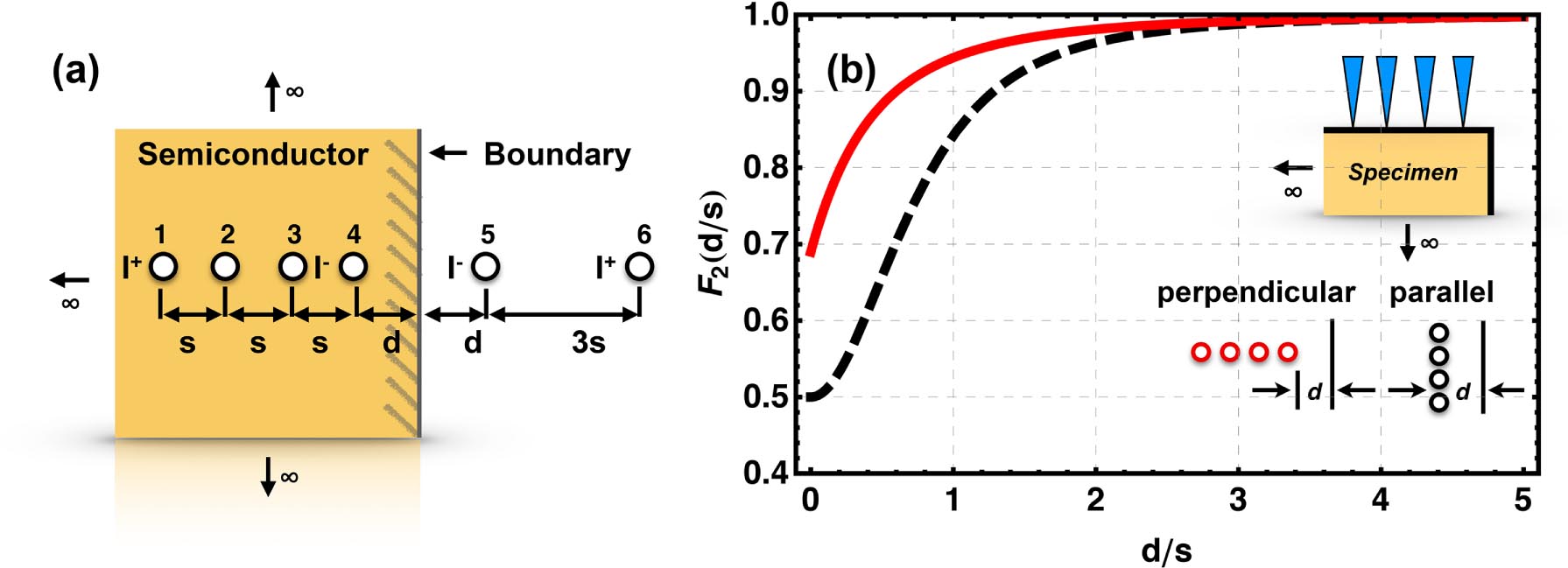
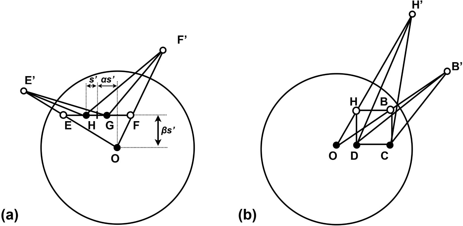
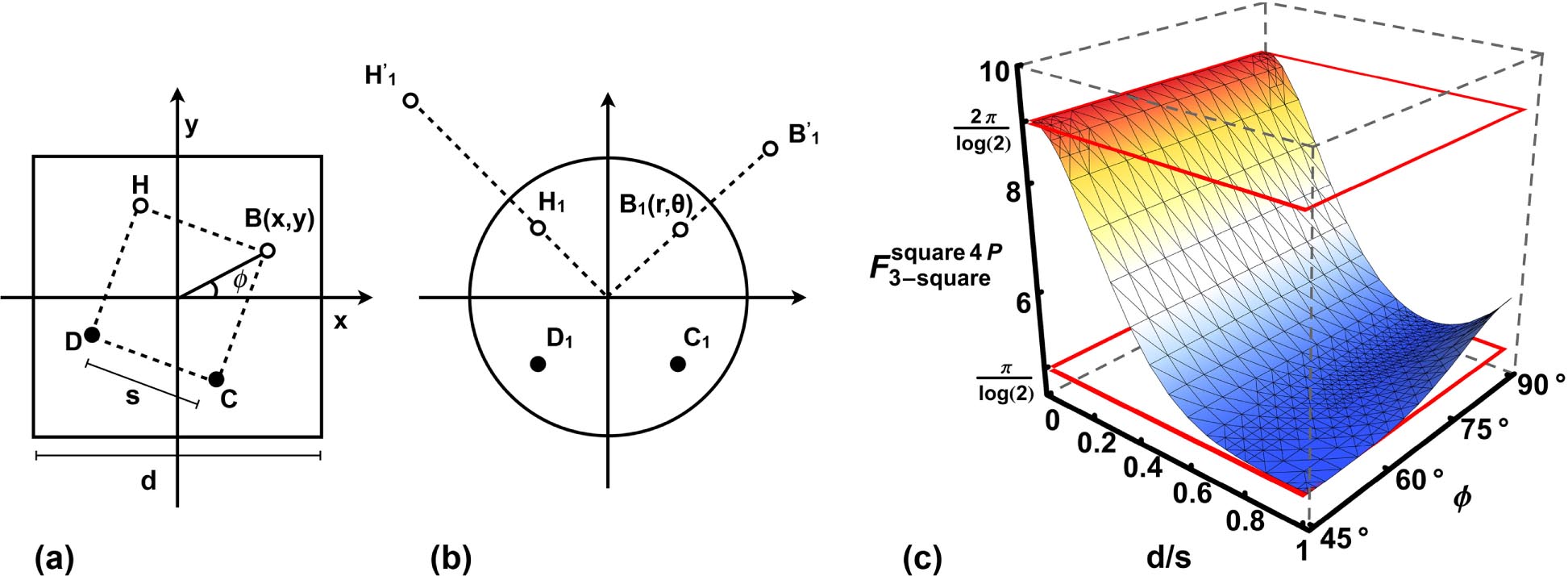
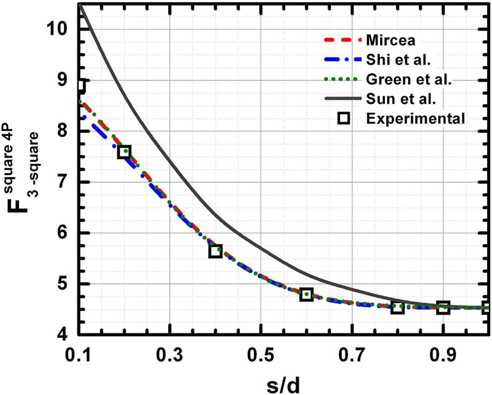
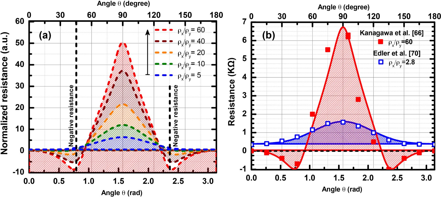
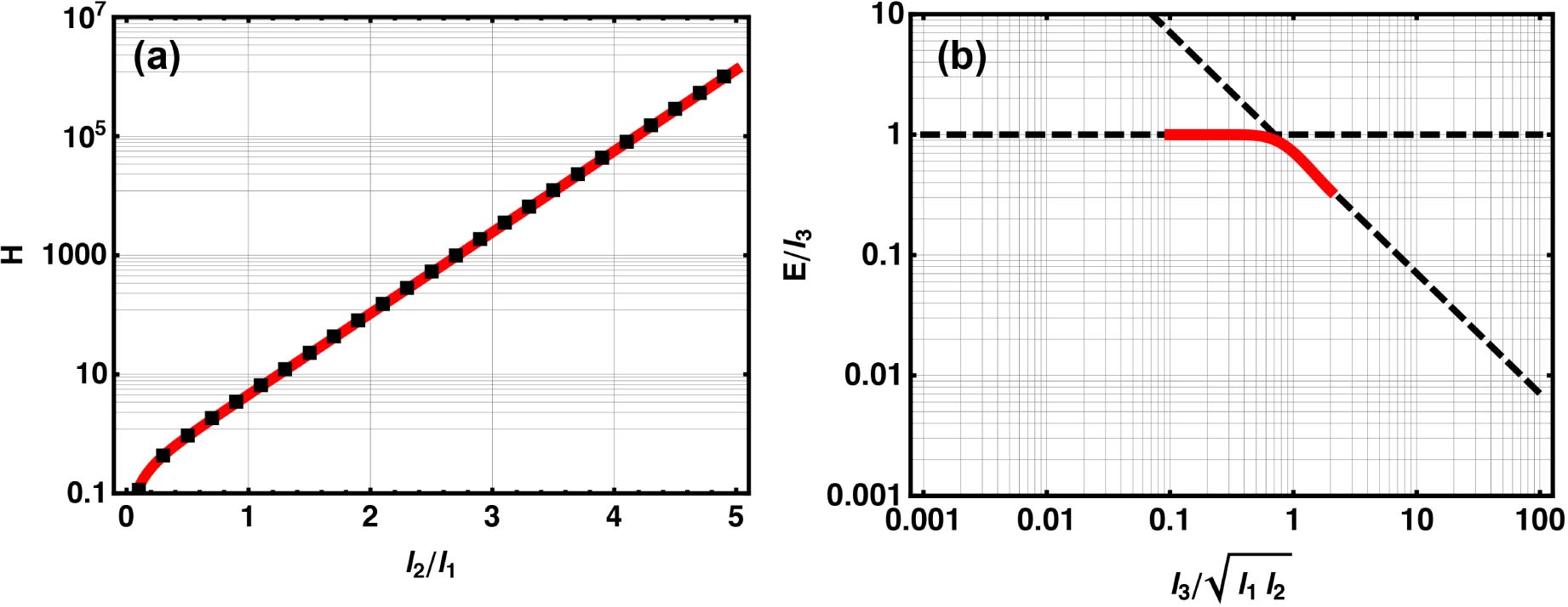
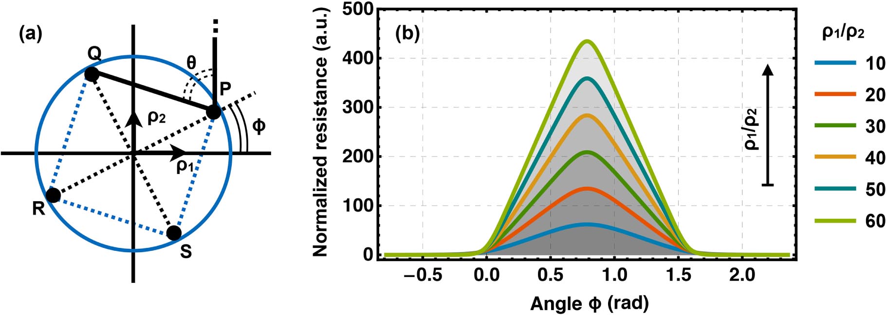
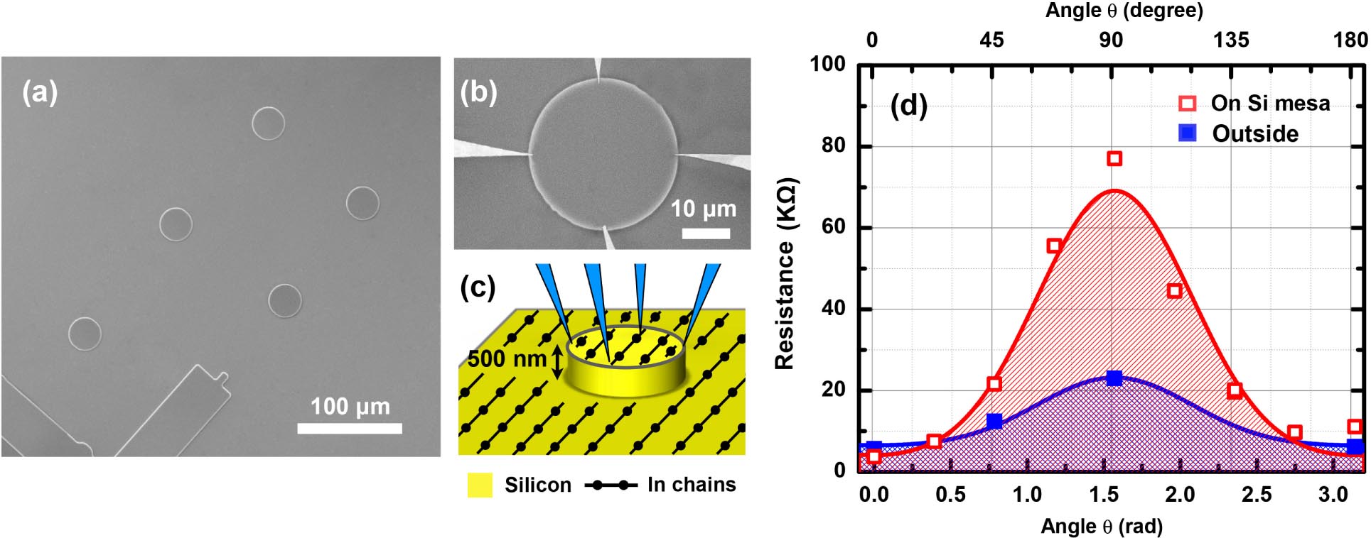
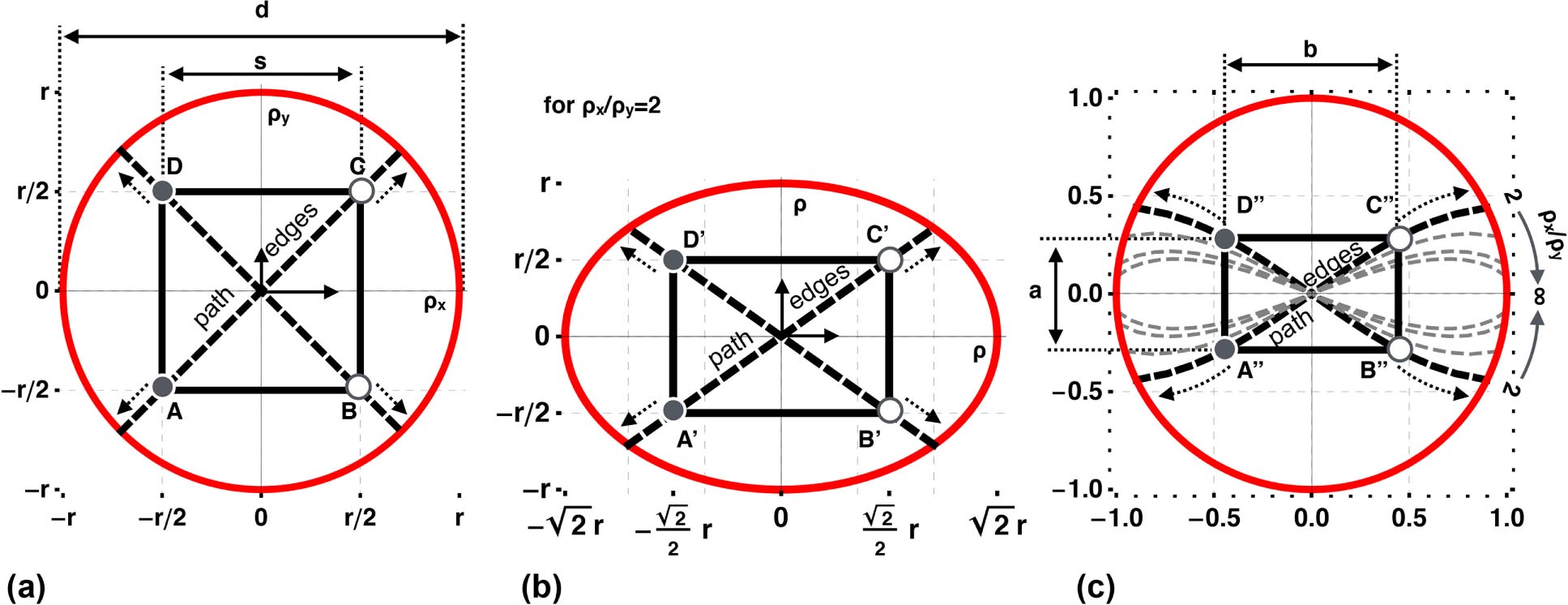
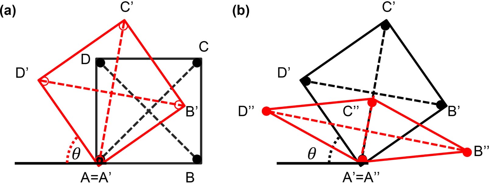
Figure D1. (a) Schematics of a 4P rectangular array onto a finite circular slice. The current sources P and Q outside the circle represent the additional image dipole introduced to mimic the boundary of the lamella. (b) Correction factor
 versus the normalized wafer diameter d/a(d/b), where a(b) is the shorter (longer) edge of the rectangle ABCD.
Download figure:
Standard image High-resolution image
The various line segments in (D.2) are obtained by simple geometric considerations (see figure D1(a))

while,

Equation (D.4) can also be expressed as a function of the side lengths, a and b, of the rectangular 4P array by noting that cos[π − α] = −cos[α] = −(2cos2[α/2] − 1) and
![${\rm cos}\left[ {\alpha /2} \right]=b/\sqrt {a^{2}+b^{2}}$](https://content.cld.iop.org/journals/0953-8984/27/22/223201/revision1/cm512562ieqn069.gif) and we immediately obtain
and we immediately obtain

If we insert (D.3) and (D.5) into (D.2) and we define the aspect ratio of the rectangle r = a/b, we finally obtain a compact expression for the voltage drop Vy between A and D as a function of the geometric parameters of the rectangular 4P probe array, which reads

with x = d/b. We can thus define the correction factor
in the following form:

Hence, the measured resistance Ry reads

It is evident that (D.8) again reduces to that of a square (see (3.13)) for r = 1. Equation (D.7) is plotted as a function of the normalized wafer diameter (x = d/b in figure D1(b), also revealing the effect of the aspect ratio r of the rectangle, which becomes obvious. The interval of existence of the function
shrinks as the rectangle aspect ratio increases.
If we rotate the rectangle by 90° (equivalently exchange the current and voltage probes), an equation similar to (D.8) results in

where
is now a function of x' = d/a

It is easy to prove that
 and (D.8) and (D.9) differ only for the logarithmic factor (in addition to the resistance term Rx, y). Figure D1(b) thus shows the trend of correction factor
irrespective of the adopted configuration for the current and voltage probes.
and (D.8) and (D.9) differ only for the logarithmic factor (in addition to the resistance term Rx, y). Figure D1(b) thus shows the trend of correction factor
irrespective of the adopted configuration for the current and voltage probes.