
Abstract
The Sb(111) surface was studied with helium atom scattering (HAS). Elastic HAS at different energies of the incident helium beam (15.3, 21.9, 28.4 meV) was applied for structural investigations. The lattice constants derived from the positions of the observed diffraction peaks up to third order were found to be in perfect agreement with previous structure determinations of Sb(111). The observed diffraction patterns with clear peaks up to second order were used to model the electronic surface corrugation with the GR method. As an estimation for the attractive part of the interaction potential a well depth of (4.0 ± 0.5) meV was found. Best fit results were obtained with a corrugation height of 12–13% of the lattice constant, which is rather large compared to other surfaces with metallic character. Intensity measurements of the specular peak as a function of incident energy were analysed to determine the distribution of terraces on the surface. The results show a quite flat Sb(111) surface and a step height of 3.81 Å of the remaining terraces.
Export citation and abstract BibTeX RIS
1. Introduction
As one of the essential components in the newly discovered group of topological insulators [1], the semimetal antimony (Sb) has recently attracted significant interest. The main feature of this group is the existence of metallic surface states, which appear due to the topology of the electronic bands despite the insulating behaviour of the bulk [1–3]. Similar topological surface states at the antimony surface have been the subject of several experimental investigations (angle resolved photoemission spectroscopy (ARPES) [4–7], scanning tunnelling microscopy (STM) [8]) as well as theoretical studies [9, 10]. Furthermore, it has been shown that Sb nanofilms are interesting candidates for applications in spintronics due to the effects of reversible spin polarization and tunable bandgaps [11, 12]. Another application of Sb(111) was found in a recent STM study. It was shown that Sb(111) electrodes in aqueous electrolyte solutions do not undergo quick surface reconstruction processes and can be used for future studies of two-dimensional adsorption layer formation processes of different organic compounds in ionic liquids [13]. Besides studies which focus on the characterization of the geometrical and electronic structure, thermal desorption spectroscopy shows indications for a considerable hydrophobic character of the Sb(111) surface [14]. The surface dynamics, namely the surface phonon modes of Sb(111) as well as the influence of electron–phonon interaction, have been calculated using density functional perturbation theory [10]. However, no further investigations of the surface dynamics have been reported so far. Due to the lack of experimental data, probing of Sb(111) with particles other than electrons is long overdue.
As a strictly surface sensitive technique, helium atom scattering (HAS) allows the investigation of the surface structure and dynamics of various materials [15]. Although semimetals have interesting features, such as being much better conductors at the surface than in the bulk, and play an important role in the case of topological insulators, only two of them have been studied with HAS so far. First, structural corrugations as well as gas–surface potentials of carbon allotropes (graphite and graphene) were investigated [16–18]. With HAS it was possible to determine the electronic corrugation of epitaxially grown graphene, which was found to be much smaller than the structural corrugation reported from x-ray diffraction or low-energy electron diffraction (LEED) measurements [17]. Second, our group used HAS to investigate Bi(111) quite recently [19]. It was shown that HAS is able to detect sub-surface phonons on semimetal surfaces in the case of a strong electron–phonon interaction [20–22]. Therewith it is possible to obtain information about the surface e–p interaction strength [20, 23]. Thus, HAS measurements of Sb(111) represent a plausible step towards a complete understanding of the group of semimetals as well as topological insulators.
1.1. Structure and properties of Sb(111)
The structure of bulk antimony under standard conditions was investigated for the first time by Bragg and Bragg with the technique of x-ray diffraction [24]. Lattice constants were determined with improved precision over the years [25–29]. Sb crystals are built in the rhombohedral A7 structure (space group  ) with two atoms per unit cell [29]. In the hexagonal notation, which is the most intuitive choice when focusing on the (111) surface, the lattice constants are a = (4.3084 ± 0.0002) Å and c = (11.2740 ± 0.0005) Å at standard ambient conditions [28, 29]. Each atom has three nearest neighbours; the distance to the three next nearest neighbours is slightly higher. This results in one of the main features of this formation, which is puckered bilayers of atoms with an orientation perpendicular to the 〈111〉 direction. Within these bilayers the bonding is of a covalent type whereas the inter-bilayer bonding is of van der Waals character. Due to these weaker inter-bilayer bonds Sb easily cleaves along the 〈111〉 direction [30]. In figure 1 a model of the Sb structure is shown with respect to the investigated (111) surface. The rhombus with side length a represents the unit cell of the surface structure in the hexagonal notation. The sixfold symmetry described by the very-first-layer atoms of Sb(111) is reduced to threefold symmetry by including second-layer atoms. Nevertheless, with the applied energies during the HAS experiments of this study, influences of other than first-layer atoms can be neglected. Hence, the 〈10〉 as well as the 〈11〉 direction, which are both shown in figure 1, can be treated as mirror planes. First investigations of the surface structure were performed with LEED [31] and reflection high-energy electron diffraction (RHEED) [32]. Recent experiments using STM [30] and photoelectron diffraction [33] revealed the detailed geometric structure of the surface, which does not undergo relevant relaxations with respect to the bulk.
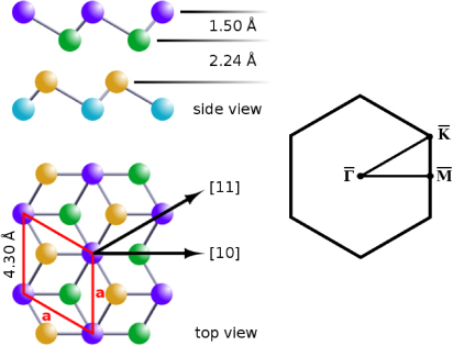
Figure 1. Sb(111) surface structure with the two high-symmetry directions of the topmost layer. The lattice constants are as determined by Bengió et al [33].
Download figure:
Standard image High-resolution imageIn contrast to the semimetallic properties of its bulk, the Sb(111) surface is found to be metallic [4, 6], which is similar to the low-index surfaces of Bi [34]. In the vicinity of the Fermi level the electronic band structure shows one hexagonal-like electron pocket at the centre of the zone and six ellipsoidal shaped hole pockets encircling this pocket [4, 5].
2. Experimental details
All experiments in this study were performed on the HAS-apparatus H.Å.N.S. (Helium Atom Nondestructive Scattering), whose properties were described in greater detail elsewhere [35]. Briefly, a supersonic expansion (pHe,1 = 50 bar → pHe,2 ≈ 10−6 mbar) through a nozzle (10 μm) and the subsequent selection of the central part of the beam with a skimmer (310 μm orifice) are used to create an almost monoenergetic He beam with an energy spread of ΔE/E ≈ 2%. By varying the nozzle temperature, beam energies between 15 and 30 meV can be achieved. After the interaction with the sample crystal placed in an ultra-high vacuum (UHV) chamber, the He atoms of the beam are detected using a quadrupole mass analyser (QMA), which is positioned at the end of a differentially pumped UHV system in a cross-beam geometry. The apparatus has a fixed 91.5° source–target–detector geometry, thus the rotation of the sample has to be changed in order to achieve measurements at different incident angles.
The sample crystal was placed on a six-axis manipulator in the main chamber. Within this chamber, the base pressure was kept below 2 × 10⁻¹⁰ mbar. The commercially available Sb(111) crystals were purchased from Metal Crystals and Oxides Ltd [36]. They had the shape of a disc with a diameter of (15 ± 1) mm and a thickness of (1.5 ± 0.5) mm.
Sample preparation was performed with a procedure based on a description of Shan et al [14]. First, the surface was sputtered with Ar+ ions (1.7 kV, 3 μA cm−2, 15 min) at room temperature. Afterwards, the sample was heated to 550 K for approximately one hour. To achieve a completely clean crystal surface, several cycles of this treatment were performed. To prove the surface quality, we used low-energy electron diffraction (LEED) and Auger electron spectroscopy (AES). Sharp LEED spots as well as clear Sb features in the AES spectrum (both shown in figure 2) indicated a surface free of any contamination. The temperature of the sample was measured using a type-K (chromel–alumel) thermocouple.

Figure 2. AES spectrum of Sb(111). The inset shows sharp LEED spots (beam energy: 38 eV) which are also indications for a clean, non-reconstructed surface. The cleanliness of the surface was checked before and after HAS measurements.
Download figure:
Standard image High-resolution imageAll measurements during this study were carried out in an in-plane scattering geometry. For that purpose the scanning direction was calibrated by adjusting the azimuthal orientation of the crystal while observing the LEED picture. Subsequently, the vertical tilt of the sample was tuned to the optimum position. For the measurement itself the polar (incident) angle θi was changed by rotating the sample around the corresponding axis.
3. Data and results
3.1. Elastic scattering
Angular HAS scans were performed along both low-index high-symmetry directions ( ) of the surface and with different energies (15.3, 21.9 and 28.4 meV) of the incident helium beam. For HAS at these energies, the turning point of the He atoms is in a region where only the very first layer contributes significantly to the relevant part of the electron corrugation above the surface. Therefore, the symmetry of the surface can be considered as sixfold.
By using incident energies of the helium beam up to 28.4 meV diffraction patterns with peaks up to third order were observable. Angular scans at this energy along the  and
and  directions are shown in figures 3(a) and (b). The measured intensity is plotted as a function of the incident angle with the zero-order diffraction peak at θi = 45.75°. Because of the large width of the peaks due to the energy broadening of the helium beam at this energy, lower incident energies (Ei,1 = 15.3 meV and Ei,2 = 21.9 meV) were used for further investigations during this study. At these energies a further test for quality and cleanliness of the surface was performed by taking a closer look at the shape of the peaks. As an example, the specular peak at Ei,1 is shown in figure 3(c) with the sample rotated in the
  direction. Since the elastic peaks are composed of a narrow coherent peak and broad diffuse elastic and multiphonon contributions [37], the fitting function consists of two Gaussian contributions. Figure 3(c) shows the narrow width of the coherent elastic contribution (red dashed line) as well as the small magnitude of the diffuse part (green dash–dotted line), which represents a good indication for a clean sample surface. Their sum (blue solid line) is in very good agreement with the measured intensity values (blue dots).

Figure 3. Scattered intensity of He versus incident angle for He diffracted from Sb(111) at a temperature of 300 K. Angular scans along  (a) and
  (b) show diffraction peaks up to third order. In (c) the narrow coherent elastic peak (red dashed line) over a small diffuse contribution (green dash–dotted line) confirms the cleanliness of the sample. The sum of these parts (blue solid line) matches very well with the measured intensity values (blue dots).
Download figure:
Standard image High-resolution imageThe experimental results of the scans with the chosen beam energies Ei,1 and Ei,2 are depicted in figures 4 and 5 (solid lines). A slight asymmetry in the angular scans occurred due to a not totally perfect alignment as well as the probable existence of steps on the Sb(111) surface [30, 38]. An optimization procedure for the sample position at each peak position yielded an estimate of 10% uncertainty for the experimentally determined intensities caused by the influence of the small misalignment. The diffraction peak positions are in perfect agreement with the expected values, confirming the already known, non-reconstructed surface structure [30, 33]. The measurements shown illustrate that a large fraction of the scattered He atoms can be found in first or higher order diffraction peaks. Thus, a contingently occurring Smoluchowski effect due to the metallic character of the surface seems negligible, since this would result in lower intensities of these features [39]. As has been found also for HAS on Bi(111) [19, 35], the electronic surface corrugation for HAS on Sb(111) has an increased importance compared to other metallic surfaces [40, 41], even when compared to the highly corrugated Ag(110) surface, where HAS experiments with incident energies up to 62 meV revealed an electronic corrugation of 0.27 Å [42]. To investigate this effect more thoroughly, the diffraction peak intensities were analysed in detail.
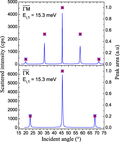
Figure 4. Scattered intensity of He versus incident angle for He diffracted from Sb(111) at a temperature of 300 K. In the upper part an angular scan along the  azimuth at an incident energy of Ei,1 = 15.3 meV is shown. The lower part depicts an angular scan along the
  azimuth at the same beam energy. The stars indicate the experimentally determined peak areas and the red squares correspond to the results of the GR method.
Download figure:
Standard image High-resolution image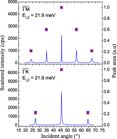
Figure 5. Scattered intensity of He versus incident angle for He diffracted from Sb(111) at a temperature of 300 K. In the upper part an angular scan along the  azimuth at an incident energy of Ei,2 = 21.9 meV is shown. The lower part depicts an angular scan along the
  azimuth at the same beam energy. The stars indicate the experimentally determined peak areas and the red squares correspond to the results of the GR method.
Download figure:
Standard image High-resolution image3.2. The surface corrugation
The He–Sb(111) surface interaction potential was determined by performing diffraction intensity calculations based on the hard corrugated wall model. Experimentally obtained peak intensities had to be compared with theoretically calculated values. As a well established approach, the GR method [43, 44] was used for this theoretical path. Furthermore, it has been shown recently that this procedure works well for similar semimetallic systems such as Bi(111) [19].
First, an appropriate model, i.e. a surface corrugation function ξ(x,y) that describes the investigated surface, is required. Considering the sixfold symmetry of the topmost layer of the surface as well as the applied incident energies of the helium beam, a two-parameter Fourier ansatz was used,

where x and y denote the rectangular coordinates and h.o. symbolizes Fourier terms up to second order. For various coefficients ξ01 and ξ11 hard wall intensities  were calculated for a sufficient number of diffraction peaks G and compared to the experimental diffraction possibilities
  . Conrad et al have shown that this approach is sufficiently accurate for fitting hard wall corrugation functions [15, 45].
Since the obtained values  correspond to a surface temperature of TS = 0 K, dynamic effects have to be taken into account. For comparison with the experimental results, the diffraction intensities at finite surface temperatures
  were calculated using

where 2W denotes the corresponding Debye–Waller factor,
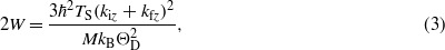
with M the mass of the surface atom, ΘD the surface Debye temperature, ħ the reduced Planck constant and kB the Boltzmann constant. kiz and kfz denote the components of the incident and final (outgoing) wavevectors perpendicular to the surface. A surface Debye temperature of ΘD = 155 K was used. This value was obtained in a recent study by our group, in which the vibrational dynamics of Sb(111) were probed with HAS experiments [46]. In this study, the thermal attenuation of the diffraction intensities of the specular and first order diffraction peaks with varying surface temperature was analysed. Measurements at four different energies of the incident He atoms were performed to find a surface Debye temperature of (155 ± 3) K. As an estimation of the mean-square displacement perpendicular to the surface, a value of (1.8 ± 0.4) × 10−2 Å2 was found at room temperature. Additionally, a well depth of (4.5 ± 0.5) meV for the attractive part of the He–surface interaction potential was obtained. In contrast to LEED experiments, where the motion of the ion cores is measured directly, in the determination of the Debye temperature with HAS experiments the fluctuation of the outermost charge density is probed. Hence, the Debye temperature obtained with HAS may differ from values determined with other techniques. Nevertheless, since the same experimental method as in the present study was applied, this result was used in equation (3). Furthermore, it is in excellent agreement with an approximation of van Delft [47], which estimates a surface Debye temperature from a given bulk Debye temperature (ΘD,bulk = 211 K [48]).
The comparison of the theoretically evaluated and corrected intensities  with the experiment was performed by determining the experimental peak areas
  . The reason for using the peak areas instead of the peak heights is the broadening of the elastic peaks caused by the energy spread of the He beam. Furthermore, additional broadening of the diffraction peaks is caused by the geometry of the apparatus, defects and the domain size effects of the crystal surface [49, 50]. Nevertheless, the elastic peaks are still narrow, lying above a broad diffuse elastic and inelastic contribution (see figure 3(c)) [37]. Thus, a sum of two Gaussian functions was used to fit the experimental peaks. Afterwards, the areas of the narrow coherent elastic peaks were taken, while each pair of peaks (G, − G) was averaged. These values were used as
  and compared with the appropriate calculations.
To determine the best fit coefficients, the amplitudes ξ01 and ξ11 were optimized by finding the best agreement between measured and calculated intensities. The intensity values of all diffraction peaks were normalized by dividing by the intensity of the corresponding specular peak. To check the accuracy of these fits, a reliability factor R,
with N the number of experimentally observed diffraction peaks, has been calculated [15].
The described fitting procedure was applied to angular HAS scans with the Sb crystal at room temperature (TS = 300 K). To account for dynamic effects arising from a finite surface temperature the experimentally found values were corrected using the Debye–Waller factor (2). The shape of the modelled corrugation is a function of the incident energy since it is based on the classical turning point of the incident He atoms [51, 52]. Therefore, two separate optimizations were performed and different parameters of the corrugation function ξ(E) were obtained for both incident energies Ei,1 and Ei,2. Uncertainties were estimated by repeating the described calculations with inclusion of the uncertainty of 10% for diffraction peak intensities, which is the dominant component of error sources. Since the He–surface interaction potential also exhibits an attractive part, the Beeby correction was used in the models to account for this attractive well [15, 53]. This approximation uses the well depth D, which is added to the energy of the incident helium atoms. Hence, the incident wavevector ki as well as Θi have to be replaced in the calculations with an effective  given by
and a smaller effective angle of incidence  with
with
Using these effective values a well depth of (4.0 ± 0.5) meV was found to result in the best fits. Compared to He–Bi(111) with a well depth of (8.3 ± 0.8) meV of the averaged surface potential [22], the determined value for Sb(111) is much lower. This can be explained by a weaker van der Waals interaction between the He atoms and the Sb(111) surface due to the smaller polarizability of Sb compared to Bi.
The peak-to-peak corrugation

for an incident energy Ei,1 was found to be ξpp(Ei,1) = (0.52 ± 0.02) Å, which is 12.1% ± 0.4% of the lattice constant a. The degree of agreement between experiment and calculation is given by a reliability factor R(Ei,1) = 0.5% according to (4). For an incident energy of 21.9 meV the calculations yielded a peak-to-peak corrugation of ξpp(Ei,2) = (0.57 ± 0.03) Å (13.3% ± 0.5%) with a reliability factor R(Ei,2) = 0.9%. The stars in figures 4 and 5 designate the peak areas ( ) while the results of the GR method are shown as squares (identical within the resolution of the figure). Both the reliability factors and the comparison of experimental and theoretical results depicted in figures 4 and 5 demonstrate the very good agreement of measured and calculated diffraction intensities and hence the quality of the modelled corrugation.
In figure 6(a) the best fit corrugation function for Ei,2 is shown. For a better illustration, cuts of the corrugation along both high-symmetry directions are shown in figures 6(b) and (c). Besides the expected structure originating in the positions of the Sb atoms of the topmost layer an enhancement of the electron density between these positions (along the  direction) seems to appear. The lateral position of this characteristic does not match with the position of underlying atoms in the bilayer. At Ei,2 (solid black line) this feature is more distinct than at lower incident energy Ei,1 (dashed blue line). More precise yet much more time-consuming ab initio calculations would be interesting to investigate this behaviour in detail.

Figure 6. (a) Plot of the hard wall potential surface for the Sb(111) surface at an incident energy of Ei,2 = 21.9 meV. The GR method was used to fit the model potential (1) to the measured helium diffraction intensities as shown in figure 5. The obtained corrugation exhibits a peak-to-peak amplitude of (0.57 ± 0.03) Å. Parts (b) and (c) show cuts along the  and
and  directions, respectively. On each x-axis the distance |r| to an arbitrary Sb atom of the topmost layer is given relative to the lattice constant a. The solid black lines represent cuts of the corrugation obtained at Ei,2 = 21.9 meV (depicted in (a)) and are compared to cuts of the corrugation obtained for an incident energy of Ei,1 = 15.3 meV (dashed blue lines).
Download figure:
Standard image High-resolution imageCompared to a surface corrugation of 10%, which was obtained for the semimetal Bi(111) [19], the values found for Sb(111) are a little higher for comparable incident energies. In general the electron density corrugation tends to be more smeared out when moving further away from the surface. Hence the higher corrugation on Sb(111) compared to Bi(111) might be a hint towards a He turning point lying closer to the surface in the case of He–Sb(111).
There exist only a limited number of direct comparisons between different atom–surface systems and actually none for different semimetallic materials. Thus, the results were compared with those obtained for group 11 metals which have been relatively well studied with HAS. Using the cut-off parameter Qc and the softness parameter β determined in these studies, the average He turning point  on the corresponding surface can be calculated according to
  [54, 55]. This shows that the average He turning point migrates further away from the surface with increasing atomic number within the group 11 metals. This fact is also supported by recent calculations which show that the distance of the jellium edge from the surface layer increases when the He–Cu(001) system is compared to He–Ag(001) [56].
In view of these facts, the larger corrugation on Sb(111) compared to Bi(111) seems to confirm this trend for these two elements within group 15. However, in order to show that the increasing corrugation is really connected with a decreasing He turning point and to prove that it can be seen as a general trend for the group 15 semimetals further ab initio calculations are needed. Such calculations appear particularly desirable, because the electron density on semimetal surfaces differs significantly with respect to that on metal surfaces. Furthermore, measurements with a much higher resolution, as can be provided by the novel helium-3 spin-echo scattering technique, would be advantageous [57].
3.3. Surface steps and terrace height
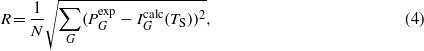
For scattering from a 'real' surface the specular intensity is usually dominated by interference effects due to waves scattered from different terraces [15]. This fact becomes evident when the intensity of the specular peak is monitored while changing the perpendicular component of the incident He wavevector kiz. Therefore the energy of the incident helium beam is varied ( ). Again, the observed peak consists of two different contributions. In contrast to the intensity of the narrow coherent peak, the intensity of the broad diffuse elastic and multiphonon contribution showed only a negligible change. Hence, monitoring of the specular peak as the sum of both contributions is an adequate approach. Such a plot of the specular peak intensity is shown in figure 7(a).
Figure 7. (a) Specular intensity as a function of the vertical wavevector transfer Δkz of the He beam. The measurement was performed along the  azimuth while the crystal was kept at room temperature. The experimental data points (open circles) were fitted using equation (8) for values between 7 and 10 Å−1 (solid line). (b) The distribution of the terraces as obtained from the best fit result.
Download figure:
Standard image High-resolution image
The intensity of the specular peak oscillates due to constructive (in-phase) and destructive (antiphase) interference between waves emerging from different terrace levels. For the specular geometry the phase difference between two waves scattered from two adjacent terrace levels is given by [58, 59]

where h is the step height and Δkz is the wavevector transfer perpendicular to the surface. For φ = 2πn an integer value of n gives rise to in-phase scattering whereas a half-integer value of n causes antiphase scattering. When the incident energy of the He beam meets one of these conditions maxima or minima are observed. This periodic change in the intensity is superimposed by the attenuation of the specular intensity due to the Debye–Waller effect (see (2)) with increasing kiz = kicosθi [58].
The experimental data points (open circles) in figure 7(a) show the measured intensity of the specular peak on Sb(111) versus the perpendicular wavevector transfer Δkz. Since for the specular scattering geometry Δkz = 2kiz holds, Δkz is varied by changing the energy of the incident He beam via the nozzle temperature. As the intensity of the incident He beam depends on the nozzle temperature TN via  [60], the measured intensity has been corrected for this factor.
In a first attempt, the intensity variation can be described by a simple model which assumes the coherent overlap of plane waves that are emerging from different terrace levels. The scattered specular intensity as a function of Δkz is then given by [58, 59]
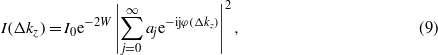
where I0 is the intensity of the specular peak for an ideal surface without steps. φ(Δkz) is the phase shift as defined in (8) and aj the visible fraction of terrace level j. The exponential prefactor accounts for the aforementioned attenuation of the intensity due to the Debye–Waller effect (see equation (2)).
However, this simple model neglects the occurrence of selective adsorption resonances whereupon the He atom is bound temporarily on the surface due to the attractive well of the He–surface interaction potential. Such selective adsorption processes give rise to peaks and dips in the scattered intensity with changing incident beam energy [15]. As can be seen in figure 7(a), various fine peaks and dips are superimposed onto the main peaks which suggest the occurrence of selective adsorption resonances. It has also been noted by Pan et al [59] that the distance between the maxima may not be exactly equidistant due to overlaying resonance effects. While an understanding of these resonance processes is crucial, e.g. in the analysis of inelastic scattering events [22], it is a rather complex task and we will restrict ourselves to an analysis of the contribution from surface steps.
Therefore, we have analysed the experimental data points in 7(a) in more detail only at higher beam energies since resonance processes become less pronounced with increasing kiz [15]. The solid line in figure 7(a) represents the best fit to the experimental data points using equation (9) under the assumption that three surface layers are visible to the He beam.
The surface step height determined from the fit is h = 3.81 Å, which agrees well with the step height of a bilayer (see figure 1). This value is somewhat larger than the value determined from STM measurements (d = (3.75 ± 0.10) Å [30]) but in perfect agreement with recent calculations [10]. The distribution of the terraces obtained by the fitting of equation (9) is depicted in figure 7(b). The best fit coefficients aj are a0 ≈ 84%,a1 ≈ 14% and a2 ≈ 2%. While these results should be considered with care due to the simplicity of the model, they indicate that the clean Sb(111) surface is quite flat. Evidence for this fact is also provided by the good quality of the diffraction patterns, as seen in section 3.1.
4. Conclusion and outlook
Elastic HAS experiments on Sb(111) at a temperature of 300 K reveal diffraction peaks up to third order. The positions of these peaks are in perfect agreement with the already known structural data [30, 33]. The rather high diffraction peaks indicate a large electronic corrugation as has been shown for the (111)-surface of the semimetal Bi [19]. The experimentally obtained diffraction intensities were compared to theoretical values, which were determined by using a hard corrugated wall model for the He–Sb(111) surface interaction potential. A potential well depth of (4.0 ± 0.5) meV provided the best fitting results when applying the Beeby correction in our calculations. The GR method was used to determine corrugation functions with a corrugation height in the region of 12–13% of the surface lattice constant at incident beam energies of 15.3 and 21.9 meV. Compared to Bi(111) this value is slightly higher, which may be an effect of the He turning point lying closer to the surface in the case of He–Sb(111). Furthermore, the obtained corrugations show enhanced values between the positions of the Sb atoms, which rise with increasing incident energy. This remarkable enhancement of the electron density has been observed also at the Bi(111) surface and its origin could be a topic of future ab initio calculations. Furthermore, possible influences of anticorrugating effects, as they were observed in scattering processes from metal surfaces [61, 62], could be included in future studies. A plane wave model was applied to intensity measurements of the specular peak, which revealed the quite flat shape of the clean Sb(111) surface. The surface step height was found to be 3.81 Å, which is in excellent agreement with recent calculations [10]. A thorough investigation of inelastic effects as well as surface phonon measurements is a logical step towards a more complete understanding of the Sb(111) surface as well as other materials with metallic surface states.
Acknowledgments
This research was supported by the European Commission and the Styrian Government within the ERDF program.