

Abstract
By combining photoluminescence, capacitance-voltage profiling and deep level optical spectroscopy, the optical and electrical signatures of the deep levels induced by N in MBE-grown homoepitaxial m-ZnO layers are identified and correlated to different physical origins. The films are electrically compensated, with carrier concentrations that decrease from ∼1 · 1016 cm−3 to ∼2 · 1015 cm−3 as a result of increasing N incorporation. Regardless of the presence of N, an intrinsic trap is found in all films at EV + 0.25 eV, most likely related to VZn defects. More interestingly, N induces three new deep levels close to the valence band whose bandgap position is electrically observed to be at EV + 0.48 eV, EV + 0.17 eV and EV + 0.12 eV. The deepest trap at EV + 0.48 eV correlates well with a N-induced level observed in previous studies on both ZnMgO and ZnO films. The EV + 0.17 eV trap behaves as a minority (hole) carrier trap, and can be uniquely correlated with the acceptor level involved in the N-induced DAP emission observed in the photoluminescence spectra. Finally, the shallowest level at EV + 0.12 eV shows an electrical signature completely distinguishable from the EV + 0.17 eV level, and dominates the deep level spectra after N-incorporation with a trap concentration of ∼1.2 · 1015 cm−3.
Export citation and abstract BibTeX RIS
1. Introduction
Zinc oxide has been a promising material for the development of oxide-based optoelectronics for a long time [1], although p-type doping still remains elusive, reports of p-type material are scarce and lacking a clear explanation for the origin of the induced acceptors [2–6]. Despite the known difficulties due to issues of doping asymmetry [7] , many approaches have been proposed, N being one of the most used dopants for p-type doping. However, the simple substitutional NO level has been shown to be a deep acceptor, with an activation energy of 1.2–1.4 eV above the valence band (VB) [8–10]. There is clearly an unresolved issue regarding the presence of acceptor levels related with N, which compensate the material without reliably changing conduction from its intrinsic n-type to p-type. Indeed, many reports of N-related acceptor levels observed by optical techniques can be found in the literature [2, 3, 5, 6, 11–13], but a direct electrical observation of the trap energy of the N-induced levels is required to uniquely identify the mechanisms leading to carrier compensation.
Indeed, direct electrical quantification of the acceptor energy and concentration in material with a residual n-type concentration is a difficult issue. Traditional Deep Level Transient Spectroscopy (DLTS) cannot be used to measure levels close to the VB in this type of material, requiring the use of optical excitation to generate minority carriers that become trapped at these shallow traps. Only one report from Muret et al [12] can be found for the case of N in ZnO, yielding activation energies (since the measurement is based on the thermal emission of carriers) and not direct trap energy levels. By using Deep Level Optical Spectroscopy (DLOS), these problems can be circumvented, since both direct trap energy and concentration values can be obtained for shallow traps close to the VB in n-type material.
Moreover, using high quality material with a low residual electron concentration is key to understanding the generation and role of acceptors, so that the net carrier concentration is low not because of auto-compensation by intrinsic defects, as previously observed for ZnMgO [14], but because of the presence of new acceptor levels introduced by the N dopant. Previous studies in MBE material report that non-polar orientations, especially m-plane homoepitaxially grown films, show the lowest residual carrier concentration with high crystalline quality and very low intrinsic defect and impurity concentrations [15, 16]. Thus, in this article we attempt to shed light on the traps generated by N doping in homoepitaxial m-plane ZnO with low residual electron concentrations, grown under the best available conditions, in order to gain a complete picture of the electrical compensation mechanisms that result from N incorporation.
2. Experimental details
Four samples were grown homoepitaxially by plasma-assisted Molecular Beam Epitaxy (MBE) on non-polar m-plane hydrothermal ZnO substrates from Tokyo Denpa. One sample was kept undoped (reference sample), whereas the three remaining samples were grown with increasing N concentrations (labeled during this study as low, mid and high N, respectively). From previous calibrations using SIMS under equal growth conditions and substrates [11], the N concentration in the films ranges from ∼1017 cm−3 in the low N sample, to ∼1019 cm−3 in the high N sample. The layer thickness was chosen to be large enough (1.5 μm) to attempt keeping the depletion region fully enclosed within the epilayer to try to avoid the electrical compensation of the films.
In the unprocessed films, continuous wave photoluminescence (PL) spectra were measured at low temperature (8 K) using a 325 nm He-Cd excitation laser under a backscattering configuration and a 1 m monochromator. Schottky diodes were processed on top of the homoepitaxial ZnO layers by depositing 100 Å-thick Au semitransparent circular contacts with a diameter of 200 μm. Prior to the metal deposition, a standard 1 min treatment in H2O2 was carried out, in order to improve the device rectification behavior [17]. Coplanar to the Schottky contact, an annealed 1000 nm-thick Ti/Al/Ti/Au extended ohmic contact was processed. The current-voltage (IV) characteristics of the Schottky diodes were measured to assess the impact of N in the basic device characteristics. Prior to any electrical measurement the diodes were kept in the dark and at room temperature, in order to avoid any persistent photo-induced effects. The resulting measurements were analyzed using custom software to obtain basic parameters such as Schottky barrier height, ideality factor and series (RS) and contact (RC) resistances. These parameters are summarized in table 1, and will be analyzed in the following section.
Table 1. Electrical characteristics from the Schottky diodes used for the capacitance measurements.
| Sample | Ideality factor | Barrier height (eV) | Rs (Ω · cm2) | Rc (Ω · cm2) |
|---|---|---|---|---|
| Undoped | 1.3 | 1.0 | 0.4 | 9.5 · 107 |
| Low N | 1.2 | 1.2 | 6.1 · 101 | 4.2 · 109 |
| Mid N | 2.4 | 1.1 | 1.6 · 102 | 2.3 · 109 |
| High N | 2.8 | 1.1 | 1.1 · 103 | 4.1 · 109 |
In order to determine the carrier concentration and conduction type, capacitance-voltage (CV) profiles were recorded for all samples using a Boonton 7200 capacitance meter at 1 MHz. For measuring at lower frequencies, a Stanford Research lock-in amplifier (model 530) was used. Analysis of the resulting CV profiles was carried out using custom software, obtaining both carrier concentration and depletion region width.
DLOS spectra were measured by illuminating the samples using monochromatic light obtained from a 1000 W Xe lamp in combination with a ¼ m monochromator, controlled with a fast optical shutter. Photocapacitance values were measured using the Boonton 7200 capacitance meter. All measurements were carried out at 1 MHz, since the quality factor under illumination was good enough (Q > 1), and by using a high probing frequency the signal to noise ratio is increased. However, the noise level was still large and no photocapacitance transients could be recorded, thus limiting the study to the steady state photocapacitance (SSPC). The diodes were illuminated at each energy for 300 s under reverse bias conditions (Vbias = −0.5 V), and then the steady state value of the photocapacitance ( was recorded during illumination. A 30 s-long filling pulse in the dark at 0 V was used between consecutive energy steps. All the measurements were carried out at room temperature.
In the SSPC spectrum, positive onsets correspond to the majority carrier emission from a trap to the band leading conduction (for this paper, the conduction band –CB–), in the absence of competing thermal emission effects (it is important to highlight this point, since it will be relevant in the discussion of the results). Minority carrier emission to the opposite band yields onsets with the opposite sign. Thus, the trap energy can be obtained by subtracting the onset energy from the bandgap energy, and referencing it to the opposite band. For example, a level that appears with an onset at Ephoton = 3.0 eV in an n-type material with a bandgap of 3.4 eV will yield a trap energy of ET = EV + 0.4 eV, close to VB. Using the total capacitance change induced by a trap in the SSPC spectrum, the concentration for the trap can be obtained using equation (1) [18]

where the value for  is obtained from the CV profiles, as previously described. This equation assumes that the change in photocapacitance under illumination, (ΔC =
  − C0), is small compared to the initial dark capacitance (C0), i.e.,
  Physically, this condition implies that the change in the carrier concentration upon photoexcitation of a trap is smaller than the steady value in the dark [19]. Concentrations obtained from equation (1) for traps found in the lower half of the bandgap in the n-type material are lower bounds [18, 19].
3. Results
3.1. Optical characterization
As a first step, the PL spectra of the sample series was analyzed at 8 K (figure 1), where two well distinct energy regions can be observed. The region at 3.36–3.37 eV shows sharp excitonic peaks in all films except for the highly doped one due to its lower crystalline quality. In this film, and as a result of its low PL intensity, a group of sharp peaks separated at a constant energy of 72 meV becomes evident. These peaks also affect the spectra of the mid N sample and appear at an integer number of the LO phonon energy (72 meV) below the laser pump energy (3.815 eV) as a result of resonant elastic Raman scattering. Indeed, the laser pump energy happens to be almost exactly 6xLO above the free exciton energy (3.377 eV). The dominant excitonic peaks that appear in the 3.36–3.37 eV region thus arise from donor-bound excitons (DX) [20]. These excitonic emissions may arise both from the epilayer and from the ZnO substrate, especially in the undoped sample where the carrier diffusion length is expected to be much larger and the electron-hole pairs may reach the substrate and recombine there. In the N-doped samples, the fact that the DX emission decreases with increasing N concentration may be indicative that it does originate in the epilayer.
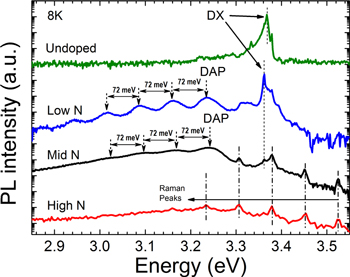
Figure 1. Photoluminescence spectra for the ZnO:N films at 8 K. In the mid and high N samples the peaks due to resonant elastic Raman scattering are indicated.
Download figure:
Standard image High-resolution imageThe major change in the PL spectra that results from N incorporation is the appearance of a prominent and broad donor-acceptor-pair (DAP) emission at 3.234 eV, with well-defined LO phonon replicas (figure 1) every 72 meV, in agreement with previous reports [3, 11, 20]. This DAP emission has a small blue shift as the N content is increased from the low to the mid N films and that is explained as a reduction in the donor-acceptor average separation [11]. In the high N sample the DAP is not clearly observed, but the broad weak PL signal is still centered at the DAP energy around 3.24 eV.
3.2. Basic electrical characterization
Table 1 summarizes the results obtained from the IV profiles (figure 2). The reference sample showed a Schottky barrier height around 1 eV, rising slightly to 1.1–1.2 eV for the N-doped samples. The ideality factor increased from 1.2–1.3 to 2.8 with N concentration, implying a reduced quality of the Schottky diode. The series resistance (RS) is limited, among other things, by the resistivity of the material, and rises linearly with the N incorporation (table 1), which indicates an increased electrical compensation. The undoped (reference) sample has an RS = 0.4 Ω · cm2, whereas with a low N incorporation, it rises to 61 Ω · cm2. The mid N sample shows a further increase in resistance up to 1.6 · 102 Ω · cm2, reaching a maximum value for the high N of 1.1 · 103 Ω · cm2. The contact resistance (RC) rises from ∼108 Ω · cm2 in the undoped sample to a stable value between 2–4 · 109 Ω · cm2, indicating a reduced effect of N in the ohmic contact quality.
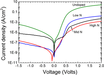
Figure 2. Current-voltage (IV) characteristics of the diodes measured under dark conditions.
Download figure:
Standard image High-resolution imageThe CV profiles both at 1 MHz and 10 kHz for all films are shown in figure 3(a), in addition to the resulting carrier concentration vs depth profiles (figure 3(b)). These profiles show that the undoped sample has a net carrier concentration around ∼1 · 1016 cm−3 and a depletion region that lays completely inside the grown layer. The low N sample shows a similar concentration to the reference sample at 1 MHz, although it decreases to ∼2 · 1015 cm−3 when reducing the probing frequency to 10 kHz. This effect suggests a low efficiency of the compensating acceptors, as will be explained in a later section of this paper.
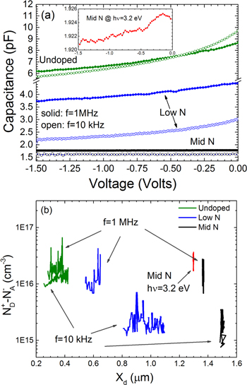
Figure 3. Capacitance-voltage profiles (a) and carrier concentration profiles (b) measured in the dark for the undoped, low N and mid N samples. Measurements were carried out both at 1 MHz –solid symbols in (a)– and 10 kHz –open symbols in (a)–. The inset in (a) shows the CV profile under 3.2 eV illumination for the mid N sample, and the resulting carrier concentration is shown in (b).
Download figure:
Standard image High-resolution imageThe mid N sample could not be effectively measured in the dark, due to the high compensation that totally depletes the grown layer at 10 KHz, as can be observed in figure 3(b). However, under illumination above the mid-gap (concurrent with the start of the DLOS spectra), the depletion width shrinks sufficiently and the CV can be effectively measured (not shown), giving a concentration of ∼1 · 1016 cm−3. This value will be used on the trap concentration calculations for this sample, since it is more accurate than the one measured in the dark, because the capacitance values used in equation (1) are obtained with DLOS, i.e., under illumination. Indeed, and in order to clarify the region being probed by DLOS, a CV spectra under 3.2 eV illumination is shown in figure 3(a), where it can be observed that the depletion layer is confined entirely in the epilayer, yielding a value of 1.3 μm. Moreover, by calculating the Debye screening length (around 25 nm), the obtained value can be considered an accurate estimation of the real depletion depth [21]. The high N sample was so heavily compensated, as indicated by the large series resistance (table 1), that its capacitance remained unchanged under any bias or illumination conditions. Thus, this sample was fully depleted and could not be analyzed by DLOS.
3.3. DLOS measurements
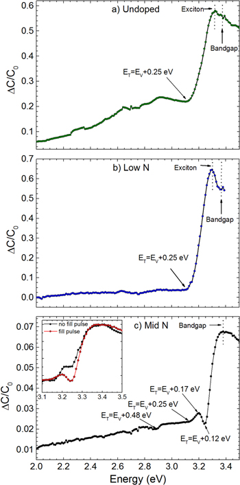
Figure 4 shows the SSPC spectra for the three samples that were electrically measurable (undoped, low N and mid N). It can be observed how both the undoped and low N samples show a significant decrease of photocapacitance above the exciton energy (∼3.31 eV). Indeed, a large increase in photogenerated carriers raises the conductivity of the diode, thus degrading the quality factor for the capacitance measurement, affecting the measured capacitance value. Nevertheless, and regardless of the presence or absence of N, all three samples show a level at EV + 0.25 eV, which for the reference and low N samples is the only trap that can be uniquely resolved.
Figure 4. DLOS spectra for the undoped (a), low N (b) and mid N (c) samples at 1 MHz and room temperature. The inset in (c) shows the normalized photocapacitance spectra from the mid N film measured with and without an electrical fill pulse.
Download figure:
Standard image High-resolution image
In the case of the undoped sample, several levels show up deeper in the bandgap (figure 4(a)). However, they cannot be resolved due to the high sensitivity to illumination of the recorded SSPC spectra, which mixes the signatures from the levels with the lamp intensity variations arising from the Xe discharge lines. These levels account for nearly half of the total capacitance change of the sample, i.e., for the total trap concentrations. Using the carrier concentrations from the CV analysis, and by applying equation (1), a lower bound trap concentration for the EV + 0.25 eV level of ∼1.4 · 1016 cm−3 is obtained, being the rise in photocapacitance affected by the degradation in the quality factor because of the excitonic absorption.
As for the low N sample, the aforementioned levels deep in the bandgap can hardly be observed, suggesting a reduction in their concentration with N incorporation. In this sample, only the level at EV + 0.25 eV is clearly observed (figure 4(b)), as in the reference sample. Similarly, a degradation in the quality factor for the capacitance measurement appears above the excitonic absorption energy. Therefore, the concentration for the trap is only a lower bound, giving a very similar value of ∼1.2 · 1016 cm−3.
In the mid N sample, the EV + 0.25 eV level is still observed but its trap concentration cannot be easily calculated due to the close proximity of a new level (figure 4(c)), which masks the associated rise. Considering the small increase this level generates in the spectra, an approximate concentration of ∼4 · 1014 cm−3 is obtained. However, it is important to note that because of the high electrical compensation already mentioned for the sample, the depletion region remains unchanged until a trap with a concentration high enough is photoexcited, causing an increase in the carrier concentration and a reduction of the depletion region width. Under these conditions the diode capacitance starts to be measurable, as it can be clearly observed in figure 4(c), in which ΔC/C0 has risen already to a value of 0.02 at the start of the first distinguishable level (EV + 0.48 eV). This is a direct indication that the steady state value of the photocapacitance ( has changed respect to the dark value (C0), which indicates that the depletion region width is being modulated, and thus the epilayer is no longer frozen out as it was under dark conditions. Therefore, the notion that more levels are present deeper in the bandgap cannot be discarded. This may be the reason why the energy level associated with the NO substitutional, which should be present at ∼EV + 1.2 eV [8–10], is not observed. It is also important to note that in DLOS all traps found within the depletion region and below the Fermi level contribute to the photocapacitance, independent to their distance from the depletion region edge. In our samples, the Fermi level is above the midgap, and the Schottky built-in voltage (∼1 V) plus the applied bias (0.5 V) is lower than half the bandgap. Thus, the contribution of the photoexcited traps (all found close to the valence band) to the photocapacitance is present from the depletion edge up to the surface, being the space charge region located entirely in the epilayer.
The most interesting result related to the N incorporation is the presence of three new traps that show up in the spectra under illumination energies of Ephoton = 2.89 eV (EV + 0.48 eV), 3.20 eV (EV + 0.17 eV) and 3.25 eV (EV + 0.12 eV). The level at EV + 0.48 eV is clearly not present in the reference sample without N. By using equation (1), its concentration can be calculated to be ∼1 · 1014 cm−3, which is very small compared to the incorporated N concentration, albeit related to it. However, this concentration must be taken as a lower bound, since, as we mentioned earlier, the sample is depleted in the dark and for lower illumination energies, and the total change in capacitance can be easily underestimated. As will be explained in the discussion, this level has already been observed using DLOS in N-doped MOCVD-grown ZnMgO [13].
The next N-induced trap appears in the SSPC spectra as a decrease in capacitance change at Ephoton = 3.20 eV (figure 4(c)), only when a voltage fill pulse of 0 V is applied as detailed in the experimental section. When the DLOS spectrum is recorded without a voltage fill pulse, i.e. under a constant −0.5 V reverse bias, this negative step disappears (figure 4(c), inset). Thus, we conclude that the voltage fill pulse is responsible for the negative step. This can be understood as a result of the competition between the majority (electron) carrier photoemission to the CB and minority (hole) carrier thermal emission to the VB [19]. Indeed, its shallow position with respect to the VB (EV + 0.17 eV) is consistent with thermal hole emission to this band at RT. Since the sample is fully depleted in the dark, a significant amount of holes may exist to compensate the material, which can be trapped during the electrical fill pulse. Thus, we can conclude that this negative onset can be related to a hole trap found at EV + 0.17 eV.
The shallowest trap, linked to the last onset observed in the SSPC spectrum, is located at EV + 0.12 eV and accounts for most of the capacitance change shown by this sample. Using equation (1), a trap concentration of ∼1.2 · 1015 cm−3 is obtained, which is still over three orders of magnitude lower than the N concentration in the sample. Since this trap is also the shallowest among all the traps with respect to the VB, it is key to understanding the effect that the growth under N has on these homoepitaxial films. Its potential physical origin will be discussed in the following section.
4. Discussion
From the combination of PL, CV and DLOS it can be observed that N plays an important role in the deep level distribution, reducing the intrinsic carrier concentration, but without achieving p-type conductivity. Next, we review all of the electrically observed traps, their relation to the PL bands, and their potential physical origin.
4.1. The intrinsic EV + 0.25 eV trap
In all samples, including the N-free reference sample, a trap at EV + 0.25 eV is observed, indicating that it is not related to N, which suggests an intrinsic defect that is responsible for the whole capacitance change close to the VB. As has already been described, for the undoped and low N samples, determining the concentration for this trap is largely affected by the excitonic absortion that degrades the capacitance measurement by increasing the conductivity. Nevertheless, a lower bound concentration of ∼1.4 · 1016 cm−3 is obtained. This trap matches the hole trap reported by Muret et al [12] at EV + 0.28 eV (labeled HT4 in his paper) in N-doped ZnO samples, using optical minority carrier transient spectroscopy (O-MCTS). In their work they suggest that this hole trap is not related to N, since its Arrhenius plot matches well with that from a similar level observed in undoped samples by other groups. Their measured concentration, ∼2 · 1016 cm−3, agrees quite well with our measured concentration (∼1.4 · 1016 cm−3), clearly showing that this level is the dominant intrinsic trap close to the VB in m-ZnO. The difference in energy between HT4 (EV + 0.28 eV) and our result (EV + 0.25 eV) could arise from the experimental error bar as well as the fact that DLOS yields the actual trap energy in the bandgap, whereas O-MCTS yields the activation energy that assumes, among other things, that the trap capture cross section is temperature independent [19].
Zinc vacancies have been proposed as an intrinsic defect creating a level with a very similar energy. Janotti et al [22] calculated this level to have a transition energy ranging 0.08–0.45 eV from the VB, depending on the calculation method. More recently, Bang et al [2] calculated this transition to be EV + 0.17 eV. In their review, the intrinsic VZn defect is more likely to be found in O-rich samples, with a much shallower energy (closer to VB [22, 23]) and lower formation energy. However, since these energies come from different calculation methods and conditions, their value must be taken with caution. Moreover, Hierro et al [14] also reported a level at EV + 0.28 eV in undoped ZnMgO grown by MOCVD in sapphire substrates that is responsible for the compensation measured in the samples, showing a large concentration. Gür et al [24] also found a level at EV + 0.3 eV in both ZnO and ZnMgO films grown by MBE on sapphire. This level was, as in our case, the dominant onset in the DLOS spectra, driving the majority of the capacitance change, further confirming the common intrinsic origin for the trap. In addition, unpublished work from our group also shows that this level is present in undoped homoepitaxial ZnO grown in a- and r- planes, which combined with the former reports, indicates that a level at EV + 0.25 eV is indeed an intrinsic level independent of the growth method and substrate orientation.
4.2. The N-induced EV + 0.48 eV trap
This trap starts to be observable in the mid N sample suggesting a relationship with N incorporation. Moreover, its concentration is quite low, ∼1 · 1014 cm−3, indicative of a reduced impact in the electrical compensation shown by this sample. Several levels have been previously reported by Muret et al [12] by O-MCTS with similar trap energies. Their HT5 level yields an equal energy of EV + 0.48 eV, although with a much higher concentration. However, and because of the error bar, our level could also correspond to their HT6 or HT7 traps, with energies of EV + 0.466 eV and EV + 0.503 eV, respectively. Also, a previous report from our group [13] shows a similar trap at EV + 0.47 eV in MOCVD-grown Zn0.9Mg0.1O:N films measured by DLOS, whose concentration increases with increasing N exposure during growth.
4.3. The N-induced EV + 0.17 trap
The level at EV + 0.17 eV is only observable as a reduction in the overall capacitance in the DLOS spectra. As already explained in the previous sections, the thermal emission of trapped holes to VB dominates over the trapped electron photoemission to the conduction band, producing a decrease of the total measured capacitance. Unfortunately, this competition of emission mechanisms does not allow the quantification of its trap concentration [19], but it does imply that the defect behaves as a minority carrier trap, in this case, a hole trap.
The energy measured by DLOS is consistent with the acceptor involved in the N-related DAP emission we observe in the LT-PL (figure 1) spectra, for which there is a consensus that it is found at 165 meV above the valence band [3, 6, 11, 25, 26]. In addition, Muret et al [12] reported a level at EV + 0.19 ± 0.04 eV, labeled HT2, with a large capture cross section, related to N incorporation. Thus, this trap at EV + 0.17 eV can be linked to the N-induced DAP. We should note that this level can only be observed by DLOS in the mid N sample, although it is also likely to be present in the low N sample. However, because of the large rise in capacitance from the dominant intrinsic EV + 0.25 eV level, it may not be possible to detect the trap, even though the DAP emission to which it contributes is clearly present in the LT-PL spectra (figure 1). In previous work from our group [13], a level at EV + 0.16 eV was reported in ZnMgO films, with a concentration increasing with N exposure during growth, and related to the electrical compensation observed in the samples.
There is an open question about what is the physical origin for the acceptor that appears with the introduction of N. In the literature, many possible N configurations in ZnO have been described, although great discrepancy can be found in the calculated energy position of the acceptors they generate, which depend on the calculation method. Recently, Bang et al [2] presented a revision of the most plausible levels related to N incorporation, which provides a new canvas for the analysis of the acceptor-like levels found in N-doped ZnO samples. The simple substitutional NO level has a large activation energy, it is present deep in the bandgap [8, 10] and is also unlikely to appear in such O-rich samples as the ones presented in this paper, since formation energy increases with O-richness. Thus, it can be discarded.
In a previous section, the VZn-related level defect is proposed to be present in the N-doped samples and although it is the only level not related with the presence of N during growth it is needed for the formation of many of the other levels proposed as acceptors. Indeed, the NO-VZn complex defect proposed by Liu et al [27] with an energy level of 160 meV above the VB, may be related to the EV + 0.17 eV trap. For this complex defect a thermal activation is needed, which in our case could be provided by exposure to the growth temperature [11] during the growth time needed to reach 1.5 μm-thick layers (more than 5 h). However, recently Bang et al [2] suggested that the NO-VZn complex has a paramagnetic nature that, when taken into account in the calculation, yields a much deeper trap energy in the bandgap (EV + 0.87 eV) [2].
Three defects involving a molecular form of N have also been proposed in the literature. The simplest one, (N2)Zn, with an activation energy of EV + 0.22 eV is also the one with the largest formation energy [2]. It is thus unlikely to be the defect responsible for any of the N-related levels found in the present study. Another one, involving oxygen, (NO)Zn, shows a much lower formation energy with a similar activation energy (EV + 0.23 eV). Lastly, the level with the lowest formation energy, (NH4)Zn, has an energy of EV + 0.18 eV, but needs the presence of large quantities of H, which is not the case for the samples presented in this paper, grown by MBE using N2 as the dopant source.
4.4. The N-induced EV + 0.12 trap
The new level at EV + 0.12 eV is not directly observed in the PL spectra, albeit being dominant in the photocapacitance measurement for the mid N sample. However, to understand its origin one has to account for the spatial effects that arise from the fact that this sample is depleted in the dark, and only under illumination can the depletion region be slightly modulated with the AC probe signal. Thus, the region being measured during DLOS is close to the substrate/epilayer interface, and the DLOS spectra can be influenced by the presence of structural defects originating at this interface. In order to fully distinguish the type of defect involved, minority carrier DLTS using a variable fill pulse may be needed, as reported by Hierro et al [28], where different kinetics for point defects, extended defects, and point defects decorating the extended defects can aid in this identification. Also, depth sensitive measurements could help clarify the structural origin of this defect. Unfortunately, both types of measurements cannot be performed in a film so strongly depleted like ours.
Accounting exclusively for its energy position in the bandgap, the EV + 0.12 eV trap may be related to staking faults. Indeed, Lautenschlaeger et al [29] showed that a PL band at 3.31 eV appeared when N is introduced in ZnO, and in parallel to the formation of the DAP. Their emission is likely to be the same as that shown by Schirra et al [30] to arise from a band-to-acceptor recombination (e, A). The acceptor level involved in this emission was proposed to be generated by staking faults and placed at EV + 0.13 eV, very close to the level observed in our films. More recently, Lin et al [31] clearly demonstrated that in m-plane ZnO films staking faults are responsible for the presence of a CL band at 3.32 eV. However, we do not observe this stacking fault-related emission in our films, and thus, it is unlikely that they are related. Even though the EV + 0.12 eV trap concentration is quite low, ∼1.2 · 1015 cm−3, this trap shows a sharp optical onset dominating the DLOS spectra, and it is clear that unveiling its physical origin will likely open the path to understanding how N is incorporated in the crystal.
5. Summary
From the combination of PL, CV and DLOS we have shown that the incorporation of N produces a strong electrical compensation, decreasing the measured electron carrier concentration from ∼1 · 1016 cm−3 down to ∼2 · 1015 cm−3. Under very high N incorporation (∼1019 cm−3) the 1.5 μm-thick films are actually fully electrically depleted and cannot be analyzed. This decrease in the electron carrier concentration under N exposure happens in parallel to the formation of three new traps at EV + 0.48 eV, EV + 0.17 eV and EV + 0.12 eV, in addition to the EV + 0.25 eV intrinsic level that is also found without N and that is likely to be related to VZn. This intrinsic level also dominates the DLOS spectrum under low N exposure, where a DAP band is clearly observed in the LT-PL that is also prominent in the mid N film. However, in the mid N film the new set of three shallow traps with respect to the VB can clearly be resolved by DLOS and their energy position in the bandgap perfectly placed. The EV + 0.45 eV trap correlates well with a similar trap observed in MOCVD-grown ZnMgO [13]. The EV + 0.12 eV trap is the shallowest and its presence can be clearly distinguished from that of the EV + 0.17 eV in the DLOS spectra, and indeed both traps can be linked to different sources. First, the EV + 0.12 eV trap does not correlate with any PL bands, but shows the highest concentration of all traps (∼1.2 · 1015 cm−3). Its significance in the DLOS spectra and its shallow position in the bandgap suggest that this level is crucial to understanding the microstructural changes induced by N incorporation. In contrast, the EV + 0.17 eV trap behaves as a minority carrier trap producing a capacitance signature consistent with hole emission to the valence band, and may originate at NO-VZn complexes [27]. It is also almost certainly the acceptor level involved in the N-induced DAP emission observed in the LT-PL, widely accepted to be at EV + 0.165 eV [3, 6, 11, 25, 31], and this correlates well with an electrically observed trap in N-doped ZnMgO at a similar energy [13].
Acknowledgments
The authors would like to acknowledge help from L Gura during the DLOS measurements, J Tamayo for his assistance with the PL measurements, and Prof. Pierre Lefebvre for his help in the PL analysis. Research at ISOM-UPM was funded by the Spanish Ministry of Economy and Competitiveness (MINECO) through Projects No. TEC2011-28076-C02-01, TEC2014-60173-C2-2, and Grant No. BES-2012-051882 Growth at CRHEA-CNRS was partially supported by the French National Agency through the young researcher project ANR 11-JS09-014 'HENOPOIN2'.