
Abstract
Cross section transmission electron microscopy has been used to analyse dislocation filter layers (DFLs) in five similar structures of GaAs on Si that had different amounts of strain in the DFLs or different annealing regimes. By counting threading dislocation (TD) numbers through the structure we are able to measure relative changes, even though the absolute density is not known. The DFLs remove more than 90% of TDs in all samples. We find that the TD density in material without DFLs decays as the inverse of the square root of the layer thickness, and that DFLs at the top of the structure are considerably more efficient than those at the bottom. This indicates that the interaction radius, the distance that TDs must approach to meet and annihilate, is dependent upon the TD density.
Export citation and abstract BibTeX RIS

Content from this work may be used under the terms of the Creative Commons Attribution 3.0 licence. Any further distribution of this work must maintain attribution to the author(s) and the title of the work, journal citation and DOI.
1. Introduction
The inability to control threading dislocation (TD) density in heteroepitaxial layers has held back the deployment of many materials systems for some time. Perhaps the most widely studied system is GaAs on Si [1], which was the subject of intense work in the 1980s [2] but failed to become commercially viable. There are two main problems in this materials system; thermal expansion mismatch [3], and high TD density  Since GaAs has a higher thermal expansion coefficient (5.73 × 10⁻⁶ K−1) than Si (2.6 × 10⁻⁶ K−1), if a thick epitaxial GaAs layer is fully relaxed during growth at a high temperature it cracks during cooling [1, 4]. The solution is to use a thin epitaxial layer, since there is a critical thickness for cracking of epitaxial layers [5]. The origin of high TD densities is not fully understood—there is currently no model that can predict the TD density in any materials system—but it is known to be correlated with the three dimensional islands that form in the very first stages of growth [6]. It is also known that the TD density decreases with increasing layer thickness [3, 4, 7], but unfortunately the amount of material required to obtain a technologically viable TD density ρTD < 105 cm−2 is much larger than the critical thickness for cracking. There is no process window.
Apart from simply growing thick epitaxial layers [4, 7], it is possible to reduce TD densities more efficiently by design. In particular, thin strained layers have been used to encourage TDs to move, interact and annihilate for some time [8, 9], and have become known as dislocation filter layers (DFLs). However, there are few, if any, studies looking at the effect of DFLs in detail, and this is the motivation for the work described here. It is hoped that understanding of DFLs may allow them to be optimized sufficiently to allow the production of GaAs layers on Si that are both below the critical thickness for cracking and with low TD density.
2. Experiment
A typical DFL sample structure is shown in the cross section transmission electron microscopy (TEM) images of figure 1. Growth was performed on n-doped Si (001) substrates offcut by 4° towards [110] using solid-source molecular beam epitaxy. Oxide desorption of the Si substrates was performed at 900 °C for 10 min The substrates were then cooled down for the growth of a 30 nm GaAs nucleation layer at 370 °C followed by 170 nm of GaAs at 515 °C. An 800 nm buffer of GaAs was then grown at 660 °C, the first 100 nm of which was a 5:5 nm AlxGa1−xAs:GaAs short-period superlattice. This was followed by three DFLs separated by 400 nm GaAs spacer layers. Each DFL consisted of five layers of 10 nm InxGa1−xAs separated by four 10 nm layers of GaAs. Following another 400 nm GaAs spacer layer an InAs/GaAs dot-in-a-well (DWELL) structure was grown at 510 °C, similar to that optimized on GaAs substrates.
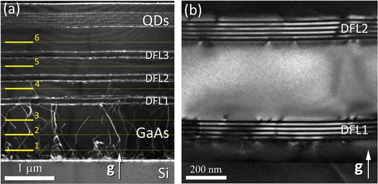
Figure 1. (a) A dark field weak beam, g, 2g 004 TEM cross section image of a typical epitaxial layer structure of GaAs on Si with three DFLs. The active region contains quantum dots (QDs), at the top of the structure. Dislocations were counted crossing the lines marked 1–6. (b) Dark field g 002 image of DFL1 and DFL2, showing the five 10 nm InxGa1−xAs layers (dark) and four 10 nm GaAs spacers in each. Misfit dislocations are visible at the upper and lower interfaces.
Download figure:
Standard image High-resolution imageFive samples were grown, listed in table 1. These samples, form two self-consistent experiments that examine the effects of (a) anneals during growth (samples R22, R23, R24) and (b) changing the composition of the DFLs (samples R24, R28, R29).
Table 1. The five samples examined in this study.
| Sample | DFL composition | Anneal type |
|---|---|---|
| UCL203 R22 | x = 0.18 | 0 |
| UCL203 R23 | x = 0.18 | 1 |
| UCL203 R24 | x = 0.18 | 2 |
| UCL203 R28 | x = 0.16 | 2 |
| UCL203 R29 | x = 0.20 | 2 |
Sample R22 had no anneals (Anneal Type 0). Sample R23 experienced Anneal Type 1; following the 100 nm SPSL in the 660 °C GaAs buffer layer, growth was paused and the sample held under an As flux. The anneal consisted of a heating ramp to 750 °C (2 min), hold at 750 °C (6 min), and cooling ramp to 660 °C (2.5 min). Samples R24, R28 and R29 experienced Anneal Type 2, consisting of anneal Type 1 plus a similar procedure after each DFL, i.e. before each 400 nm GaAs spacer layer.
The efficacy of TD filters is often assessed using techniques such as defect etching, which provides a single measurement for each growth. In contrast, here we use TEM to examine the structure in detail, in particular the changes in dislocation density through the epitaxial layer. Cross section TEM specimens parallel to {110} were prepared using standard protocols, each of which typically yielded 30–60 μm of electron transparent area along the GaAs:Si interface. A series of images were taken using bright field g 220 diffraction conditions with the specimen tilted 5°–10° from the {110} zone axis, capturing the complete structure as shown in figure 2 while covering as wide a field of view as possible. The change in TD density  through the epitaxial layer was measured by counting those which crossed six lines, as indicated in figure 1(a). Although it is not possible to give an absolute measure of
  without knowing the thickness of the TEM specimen, this technique allows relative measurements to be obtained that are statistically meaningful. In particular, by counting TDs below and above a DFL it is possible to measure the fraction removed. Importantly, the measurement relies on two assumptions. First, the thickness of the TEM specimen from bottom to top of the epitaxial structure must not change. The validity of this assumption was checked by examining the projected length of misfit dislocations in the GaAs:Si interface as well as the DFLs, and was found to be valid to better than 5% for all measurements. Second, not all TDs are visible in images obtained with a single g-vector and it is assumed that the behaviour of the invisible dislocations matches those of the visible ones. In a g 220 image, TDs with b = ½ [1–10] and ½[−110] give g · b = 0 and are invisible (two of the twelve possible Burgers vectors in a face centred cubic material). These are sessile TDs, unable to move by glide, similar to the b = ½[110] and ½[110] types (all other types being glissile on {111} planes). Numerical modelling of TDs ensembles [10] indicate an interchange between mobile and sessile TD populations, leading to a balance; thus between a sixth and a quarter of TDs are expected to be invisible in g 220 images. The aim was to count more than ten TDs at the uppermost line (typically giving counts up to a thousand at the lowest line). This was possible for all samples apart from R24, which had the lowest ρTD at the surface.
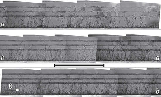
Figure 2. Montage of 13 bright field g 220 TEM cross section images (total width 48 μm) of UCL203 R22. The images join at edges a–a and b–b. The scale bar is 5 μm.
Download figure:
Standard image High-resolution imageWhile it is not possible to give an accurate measurement of ρTD, we may obtain a rough estimate from images such as figure 2. The average TEM specimen thickness is of the order of 400 nm and there are 17 TDs that can be seen to reach the upper part of the structure over the ∼50 μm width of the image. Taking into account the dislocations which are not visible in figure 2, this corresponds to a TD density of the order of one per square μm, i.e. ρTD ∼ 108 cm−2.
In addition to the measurement of TD numbers through the structure, the density of misfit dislocations,  lying at the lower and upper interfaces of each DFL was obtained from bright field g 220 images at higher magnification. The misfit dislocation density was measured from the distance that contained a hundred misfit dislocations.
3. Results
Counts of TDs at the first three lines, 300, 600 and 900 nm from The GaAs:Si interface, allows the 'natural' decrease in  in thick layers to be measured. Previous measurements of the decrease in
  with thickness h have found a behaviour described by [11–13]

i.e. a power law, where A is a constant and the exponent m has a value of −1 [11], or −2 [12, 13]. We also find that a power law provides the best fit to our data (as opposed to, for example, a polynomial or exponential decay); however all of our data was consistent with m = −½, as can be seen in figure 3 for sample R23.
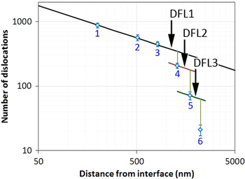
Figure 3. Log–log plot showing threading dislocation counts at the six positions in sample R23. A fit to the first three points is shown using a power law ρTD = At−0.5. The effect of the DFLs is estimated by extrapolating this law to larger thicknesses.
Download figure:
Standard image High-resolution imageSince ρTD decreases with thickness even in the absence of a dislocation filter, the efficiency of a DFL can only be measured by taking this 'natural' decay into account. Thus, the curve fit to the first three points is extrapolated to higher thicknesses as shown in figure 3. We define the efficiency of a DFL to be the fraction of TDs it removes, i.e.

where n(meas) is the number of dislocations counted at the line above the DFL, and n(predict) is the number of dislocations that would be present at that position by extrapolation of equation (1). The measured efficiency of the DFLs in all five samples is given in table 2. Errors in table 2 are based on the assumption that the spatial distribution of TDs follows a Poisson distribution, in which case the uncertainty in a count of n dislocations is n0.5. The low numbers of dislocations that are counted for the upper DFLs produce large relative uncertainties.
Table 2. Efficiency of DFLs in the five samples.
| Sample | DFL1 | DFL2 | DFL3 | Total |
|---|---|---|---|---|
| UCL203 R22 | (39 ± 6)% | (46 ± 9)% | (76 ± 30)% | 92% |
| UCL203 R23 | (40 ± 3)% | (60 ± 8)% | (67 ± 16)% | 92% |
| UCL203 R24 | (44 ± 6)% | (86 ± 30)% | (88 ± 30)% | 99% |
| UCL203 R28 | (49 ± 7)% | (65 ± 16)% | (44 ± 16)% | 90% |
| UCL203 R29 | (42 ± 3)% | (61 ± 8)% | (60 ± 13)% | 91% |
The uncertainties are sufficient to mask any correlations due to different compositions (R24, 28, R29) or anneals (R22, R23, R24). Nevertheless, it is clear from table 2 that the upper DFLs tend to be more efficient than the lower ones.
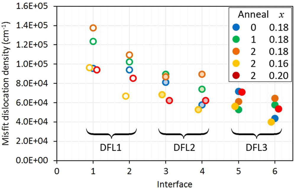
Measurements of misfit dislocation density  in the lower (L) and upper (U) interfaces of the DFLs are shown in figure 4. There is an obvious trend towards lower misfit dislocation densities in the upper DFLs, but once again any effects of composition or annealing cycle are masked by the spread in the data.
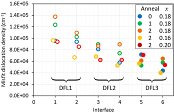
Figure 4. Misfit dislocation densities at the lower and upper interfaces of the DFLs.
Download figure:
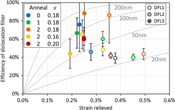
Standard image High-resolution imageFigure 5 shows the efficiency of the DFLs as a function of the total strain relieved (i.e. proportional to the total misfit dislocation density in the DFL interfaces). This shows how the lower DFLs generally do not achieve high efficiencies for the removal of TDs, despite the higher density of misfit dislocations.
Figure 5. Plot of DFL efficiency versus the total strain relieved in the DFL interfaces. Curves are also shown for the predicted efficiency at different interaction radii R = 20, 50, 100, 200 nm.
Download figure:
Standard image High-resolution image
4. Discussion
The data clearly show several trends that do not agree with simple models of the behaviour of dislocations in strained layers and the effect of DFLs [9, 11, 13], indicating that there is still much to be learned about the behaviour of dislocations en masse. For example, in the material below the DFLs we find a decrease in TD density given by

in contrast to previous work [12, 14], which found a decrease proportional to 1/h or 1/h2. The reasons for this are unclear at present, but may be related to the presence of the SPSL at the bottom of the structure, the overlying DFLs, or the different methodology used in this study.
Previous modelling [10] of interactions between mobile TDs in a strained epitaxial layer found that TD density decreases exponentially with the strain relaxed  r, i.e.

where  is the TD density immediately below the DFL, q is the fraction of encounters between TDs that lead to an annihilation (q = ¼ if there are equal numbers of all possible Burgers vectors), D is a geometrical factor (D = ½ in the case of a rectangular dislocation array), b// is the Burgers vector component parallel to the interface and R is the 'interaction radius'. Curves corresponding to equation (4) for several different values of R are shown in figure 5; it is clear that none of these curves describe the observed behaviour.
Despite the failure of the model, there can be no doubt that the basic tenet—i.e. that movement of TDs leads to reactions and annihilations—still holds. It is therefore worth examining the assumptions of the model used to obtain equation (4). In particular, the four parameters R, q, D and b// were all assumed to be constant and independent of other parameters. The results shown in figure 5 suggest that the interaction radius is not just sensitive to the strain state, as found by Fertig et al [15] but is also determined by the TD density  Furthermore, the volume of material sampled, while large by the standards of TEM, only samples a miniscule part of the entire wafer and it is possible that variations in misfit and TD density occur over larger length scales.
5. Summary and conclusions
Measurements of the number of TDs and the density of misfit dislocations have been made by analysing cross-section TEM images. Although this does not give an absolute measure of TD density  it provides valuable information about the change of
  through the structure. The technique was applied to five samples of GaAs:Si, each containing three InxGa1−xAs:GaAs DFL structures of the same dimensions, but with different annealing regimes or indium content. The DFLs in all structures removed more than 90% of TDs. This led to poor counting statistics for TDs at the top of the structure even though ∼1000 TDs were counted at the bottom of the structure, meaning that it was not possible to distinguish between the different structures in terms of the efficiency of the DFLs. Nevertheless some very useful information was obtained, in particular (1) in material without DFLs, the TD density decreases following a power law
  and (2) the efficiency of DFLs at the top of the structure tends to be higher than those at the bottom. This indicates that the interaction radius, the distance below which TDs will meet and annihilate, is sensitive to
  .
.
Acknowledgments
This work was funded by the EPSRC under grant numbers EP/J013048/1 and EP/J012904/1.