
Abstract
The sensitivity of second and third generations of interferometric gravitational wave (GW) detectors will be limited by the thermal noise of the test-mass mirrors and highly reflective coatings. Recently developed crystalline coatings show a promising thermal noise reduction compared to presently used amorphous coatings. However, stringent requirements apply to the optical properties of the coatings as well. We have mapped the optical absorption of a crystalline AlGaAs coating that is optimized for high reflectivity for a wavelength of 1064 nm. The absorption was measured at 1530 nm, where the coating stack transmits approximately 70% of the laser light. The measured absorption was lower than  ppm, which is equivalent to
  ppm for a coating stack that is highly reflective at 1530 nm. While this is a very promising low absorption result for alternative low-loss coating materials, further work will be necessary to reach the requirements of
  ppm for future GW detectors.
Export citation and abstract BibTeX RIS

Content from this work may be used under the terms of the Creative Commons Attribution 3.0 licence. Any further distribution of this work must maintain attribution to the author(s) and the title of the work, journal citation and DOI.
1. Introduction
Gravitational wave (GW) detectors are the most sensitive displacement measurement devices in the history of physics. Large Michelson interferometers with perpendicular arms were developed to search for extremely small changes in the relative distance of test-mass mirrors. These mirrors are coated to be highly reflective and form arm cavities of several kilometers in length [1]. The 2nd generation of these detectors with improved sensitivity [2, 3] is presently being implemented and is expected to make the first detection of GWs within the next two years. In the most sensitive part of the detection bandwidth, the performance of these detectors is expected to be limited by thermal noise from the optical coatings applied to the test-mass mirrors.
To reduce the impact of thermal noise on the system performance, future detectors like Advanced LIGO (aLIGO) upgrades and the Einstein Telescope (ET) are planned to operate at cryogenic temperatures [4, 5]. The requirements on the mirror-substrate material and the coatings are low mechanical loss to minimize Brownian thermal noise, low optical absorption to maintain the cryogenic base temperature and reduce background heating, as well as to avoid thermal lensing, and very accurately specified high reflectivity [6]. The mechanical loss of the presently used substrate material fused silica (FS) increases towards low temperatures [7] making FS unsuitable for cryogenic GW detector application. Crystalline silicon (c-Si) has been identified as a promising replacement material, with several attractive properties [8, 9] including a low intrinsic mechanical loss which decreases at low temperatures [10, 11]. Because of high optical absorption in c-Si at 1064 nm a change in laser wavelength is required towards longer wavelengths where the absorption decreases rapidly [12, 13]. Operation at the telecommunication wavelength of 1550 nm has been proposed as the most reasonable approach because of available high quality optical components and stable high power lasers. Amorphous SiO2/Ta2O5 coatings match the absorption requirements at both 1064 and 1550 nm but the mechanical loss is still above the proposed requirements [14].
Recently, crystalline coatings composed of alternating layers of gallium arsenide (GaAs) and aluminium gallium arsenide (AlGaAs) have been developed which show promising thermal noise and absorption properties. At 1064 nm an absorption of 12.5 ppm and a reduction of the Brownian thermal noise by a factor of three (corresponding to a tenfold reduction in the mechanical loss angle) compared to SiO2/Ta2O5 coatings has been reported [15]. These crystalline coatings have to be grown on bulk crystalline substrates with matching coating and substrate crystal structure and lattice parameters. For GW application the coatings then have to be transferred to a suitable test-mass substrate. The cavity input test masses (ITMs) for aLIGO and future GW detectors have design transmissions of about 1% while the end test-masses (ETMs) have much lower transmission in the order of a few ppm [2, 16]. For ITM transmission the laser beam will see an absorption sum from all potential absorption sources such as the mirror substrate, the substrate surfaces and the interface between the bonded coating and substrate, while the beam is basically unaffected by other sources than pure coating absorption when being reflected by the ETM.
In this paper we report absorption measurements at room temperature on a GaAs/AlGaAs coating stack at a wavelength of 1530 nm as a first step towards cryogenic crystalline coated mirrors. The coating stack was optimized for a reflectivity of  (
( ) at 1064 nm and was grown on a GaAs crystal before being transferred and bonded to a FS disc using a direct bonding procedure [15]. We measured the optical absorption of the AlGaAs coating using photothermal common-path interferometry (PCI) [17]. In our experiment we have mapped the absorption of a 4 mm × 5.7 mm area to investigate the uniformity of the coating. The coating stack which is highly reflective at 1064 nm transmits about 70% of the input laser power at 1530 nm. The ability to measure in transmission provides information of the absorption of the coating stack including any possible absorption associated with the bond between the coating and the substrate. Subsequently the measured absorption is scaled to allow comparison with the highly reflective case.
2. The experiment
The crystalline AlGaAs coating stack is identical to that described by Cole et al [15] for which a direct thermal noise measurement was made. It consists of 40.5 bilayers of alternating GaAs and AlGaAs and is optimized for high reflectivity (HR) at a wavelength of 1064 nm. A circular stack 16.4 mm in diameter was bonded to a FS disc 3'' in diameter and 1.7 mm in thickness (see figure 1(a)). We measured the optical absorption of the coating at a wavelength of 1530 nm, where the stack transmits 70% of the laser power, using the PCI technique [17, 18]. Figure 2 shows the experimental setup which was used for absorption measurements.

Figure 1. (a) Photograph of the 3'' diameter fused silica disc with the 16.4 mm diameter AlGaAs coating in the middle. (b) Schematic of the AlGaAs coated sample: the laser beam transmits through the AlGaAs coating (green), the substrate surfaces (purple), and the bulk of the fused silica substrate (blue).
Download figure:
Standard image High-resolution image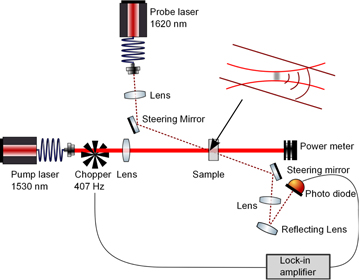
Figure 2. Photothermal commonpath interferometry (PCI) setup: a strong pump beam (red) with small waist and a weak probe beam (dark red, dotted) with large waist are converging in the coating. Due to heating caused by optical absorption, the pump beam changes the phase of a portion of the probe beam. The fraction of the probe beam which is affected by the pump beam interferes with the part of the probe beam that is unaffected. The interference becomes maximal one (pump) Rayleigh range from the pump waist and is measured by a photo detector. The pump beam is amplitude modulated using a chopper.
Download figure:
Standard image High-resolution imageSection 2.1 gives a short summary of the PCI technique. In section 2.2 the absorption as measured for the 70% transmissive coating on the FS disc is presented. Section 2.3 deals with the absorption of the uncoated surface of the FS substrate, which has to be subtracted from the total absorption. In section 2.4 a possible intensity dependence of the optical absorption is checked. Finally, in section 2.5 the absorption found for the transmissive 1064 nm optimized stack is scaled for comparison to a HR coating for 1530 nm.
2.1. Experimental setup
PCI measures the change in phase of a portion of a large probe beam ( radius for the measurements presented here) caused by the absorption of light from a small pump beam (
 ). The phase difference created by the pump beam within the probe beam is read out by measuring the interference between the light unaffected by the pump and the light which has been affected by the pump. This interference has a maximum value when measured approximately one (pump) Rayleigh range from the pump waist. The interferometric phase change measured at this point is directly proportional to the absorption of the material. The pump beam is amplitude modulated at a given frequency and a lock-in amplifier is used to recover the modulation of the interferogram at this frequency. The lock-in amplifier also provides the phase of this signal with reference to the pump modulation. This phase is determined by the diffusion of the heat from the pump absorption in the medium and by the pump beam dimensions. In the case where the transverse dimensions (characterized by the 1/e beam radius) are much smaller than the longitudinal dimensions (characterized by the Rayleigh range) of the beam, the characteristic frequency is given by
  , where D is the thermal diffusivity of the material and w0 is the beam waist. For modulation faster than this frequency the phase tends to −90°, whereas for slower frequencies it tends to
  .
.
2.2. AlGaAs coating—absorption measurement and analysis
In this section the absorption map of the AlGaAs coating is presented. First the information provided by the map of the phase signal is discussed (section 2.2.1). Afterwards the phase information is used to calibrate the amplitude signal and obtain the absorption (section 2.2.2).
2.2.1. Measurement of the phase
For the AlGaAs coating an area of 4 mm × 5.7 mm was mapped to check the homogeneity of the absorption. For the case of coating absorption, PCI and other methods which are based on heating assume an immediate heat transfer from the coating into the underlying substrate, and that the area of the substrate which is heated, and therefore affects the probe beam, is large compared to the thin coating [19, 20]. Amorphous coatings usually show a small thermal expansion coefficient ath and a small thermo-refractive coefficient dn/dT. So the phase change caused within a thin coating of only a few μm, is small compared to the phase change caused within the substrate. These assumptions are valid for amorphous, sputtered coatings for which the majority of the signal is caused by the substrate while the signal produced directly in the coating is negligible.
Figure 3(a) shows a map of the measured phase signal of the AlGaAs coating which provides two significant conclusions.
- (i)The phase varies strongly for different positions on the coating.
- (ii)The mean value of
 differs significantly from the expected phase for the FS disc of for the used chopper frequency of 407 Hz.


Figure 3. Map of the phase (a) and absorption (b) of a 4 mm × 5.7 mm area on the AlGaAs coating: (a) shows a map of the phase as a function of position on the coating. (b) Shows the optical absorption with an average of  after recalibration considering the phase information. (The white squares indicate high absorbing spots on the coating, presumably originating from dust.) (c) and (d) show a typical signal for calibrated phase (c) and amplitude (d) of a scan through the sample. The red (dashed) vertical line shows the position of the coating and the disc's back surface.
Download figure:
Standard image High-resolution imageThe variation across the coating indicates a non-uniform heat conduction of coating and substrate (for an assumption of uniform coating and substrate material parameters) which may be related to variations in the quality of the bond between the coating and the substrate. The discrepancy of the mean phase from the expected phase for FS in general shows that the signal from the coating contributes significantly to the total signal.
2.2.2. Analysis of the phase signal
Figure 4(a) shows the development of the phase with chopper frequency p(f) for one position on the AlGaAs coating. The red solid line shows a simulation  for FS. The measurement of the phase of an uncoated part of the FS disc is shown by the light green crosses (×) which is in agreement with the simulation. (The discrepancy for high frequencies is caused by low signal due to low/short heating.) The green dashed line shows the theoretical frequency dependence of the phase for AlGaAs
  and the dark blue pluses (+) represent the phase measurement for the crystalline AlGaAs coating on the FS disc which is a mixture of
  and
and  . Correspondingly the amplitude a(f) will also be a mixture of the amplitudes of FS
  and AlGaAs
  . The blue crosses (×) in figure 4(b) show a measurement of the amplitude for the AlGaAs on FS system. The total (amplitude and phase) signal for this AlGaAs coating on FS system is given by
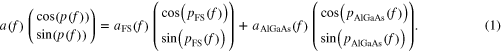
From this we get the relationships for the amplitudes

Using the phase information shown in figure 4(a) and equation (2) the measured amplitude a for the mixed signal can be separated into the amplitude signals from the FS substrate  and the AlGaAs coating
  . The light blue dots in figure 4(b) represent the part of the signal originating from the FS disc and the pink crosses (×) represent the part of the signal originating from the AlGaAs coating. The solid red and dashed dark green curves show corresponding simulations.
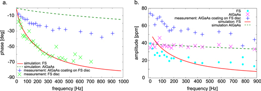
Figure 4. (a) Shows a measurement of the phase of the AlGaAs coating at different chopper frequencies (blue pluses (+)). The red solid line shows a simulation of the phase of FS which is in good agreement with measurements on an uncoated part of the FS disc (light green crosses (×)). The green dashed line shows the simulated phase for AlGaAs. In (b) the corresponding amplitude measurement is shown (blue pluses). Using equation (2) this signal was split into the separate signals for FS (light blue dots (•)) and AlGaAs (pink cosses). The red solid curve and the green dashed curve represent simulations for the amplitudes.
Download figure:
Standard image High-resolution imageFrom a measured amplitude the absorption was calculated to be  . The calibration factor K was obtained by using a FS neutral density filter (FSQ-ND02 from Newport [21]) with a coating absorption of 21.4% for calibration. For the FS fraction of the amplitude signal shown in figure 4(b), the calibration which was made with the FS sample is valid. For the AlGaAs component of the amplitude signal the absorption has to be recalibrated taking the material parameters into account which are given in table 1. An additional calibration factor calculates from
to 1.04 at 407 Hz, where DF is the dispersion function for surface absorption which describes the thermal relaxation and depends on several parameters of the experimental set up and the thermal diffusivity of the material in question. For details see [17], equation (2). The measured absorption correspondingly calculates to

Table 1. Material parameters used for the simulations of amplitude and phase. The coating material parameters used for the simulation were the average of the values for GaAs and AlGaAs, weighted by the total thickness of each material in the coating stack.
| Parameter | FS Substrate | GaAs | AlGaAs |
|---|---|---|---|
| Index of refraction n (1530 nm) | 1.44 [22] | 3.38 [23] | 2.93 [23] |
| Index of refraction n (1620 nm) | 1.44 [22] | 3.37 [23] | 2.93 [23] |
| Thermo refr. coeff. dn/dT (1/K) |
 [24] [24] |
 [27] [27] |
 [27] [27] |
| Specific heat c (J/(kg K)) | 740 [25] 330 [26] | 440.4 [26] | |
Density ρ ( ) ) |
2.34 [24] | 5.32 [26] | 3.98 [26] |
| Thermal expansion ath (1/K) |
 [24] [24] |
 [26] [26] |
 [26] [26] |
| Thermal conductivity kth (W/(m K)) | 1.38 [24, 25] | 55 [26] | 70 [26] |
The calibration factor of 1.04 indicates that for the given material parameters and the measurement frequency, weighting of coating and substrate is very similar. This varies significantly for different materials and frequencies.
Figure 5(d) shows a map of the calibrated absorption α after recalibration for each single measurement depending on the varying phase. The mean value of the absorption is  ppm (mean value and standard deviation). In section 2.5 this result is compared to the expected absorption for a highly reflective (HR) coating in which the vast majority of the light is reflected by only the first few layers of the coating.

Figure 5. (a) and (b) show the PCI signal for calibrated amplitude (a) and phase (b) of an uncoated part of surface of the FS disc to which the AlGaAs coating is attached. The red (dashed) vertical line show the position of the disc's front and back surfaces. The front surface shows higher absorption than the back surface. (c) Shows several absorption measurements on the disc's front surface measured in a line with 0.635 mm distance. Strong variations are visible with a mean value of  . (d) Shows an equivalent measurement of the absorption of the uncoated back surface. The absorption is more uniform with an average value of
  . (e) Shows the absorption of an identical, but uncoated FS disc. The absorption of this surface is
  and in good agreement with the absorption of the back surface of the coated disc.
Download figure:
Standard image High-resolution image2.3. Absorption of the (uncoated) FS disc
In a further step the absorption of an uncoated part of the coated face of the FS disc was measured. Figure 5(a) shows the calibrated absorption signal of a scan through the FS disc, figure 5(b) shows the corresponding phase signal. The red dotted lines mark the position of the substrate's front (left) and back (right) surface. The absorption of the front surface is clearly higher than the absorption of the back surface. Therefore, we measured the absorption at several positions with 0.625 mm separation on the front surface (figure 5(c)) and, after turning the disc around, repeated this measurement series for the back surface (figure 5(d)). These measurements confirmed that the absorption of the back surface is  (mean value and standard deviation) and therefore significantly smaller and more uniform than on the front surface with
  . For comparison we measured also the absorption of the surface of an identical, uncoated FS disc (figure 5(e)). The absorption of this surface was
  and in good agreement with the absorption of the back side of the coated substrate.
The origin of the absorption increase and whether we can assume a similar surface absorption increase under the coating is unknown. The only difference in storing and treatment of the samples front and back surface was the plasma cleaning procedure used prior to the bonding process. The surface roughness of the front surface was found to be higher than the back surface by 25% (root mean square roughness of  instead of
  = 1.97 nm on an area of
  , measured with a Wyko NT1100 optical profiling system which uses white light interferometry) which would not necessarily increase the absorption but might increase the susceptibility to contamination.
Therefore, we can only give an upper limit for the absorption of the coating stack by subtracting the absorption of  ppm of the back surface resulting in
  . This corresponds to an absorption coefficient of
  and an extinction coefficient of
  at 1530 nm.
2.4. Intensity dependence of the absorption
Semiconductor materials such as AlGaAs show two-photon absorption effects in which two photons are absorbed simultaneously to enable a carrier to cross the band gap. The band gap for AlGaAs is between 1.424 eV (871 nm, GaAs) and 2.16 eV (574 nm, AlAs). Therefore, we measured the intensity dependence of the absorption at one position of the coating. The intensity was varied between 78 and  . While the beam radius of
  was constant for all measurements the laser power was increased from 300 to 1760 mW. This intensity range is above the intensity for ET LF (
 ) and includes the intensity for ET HF (
 ) and aLIGO (
 ). The measurement series is presented in figure 6 and shows that the absorption of 42 ppm varies by less than
  within the studied intensity range. No significant increase at higher intensities was observed.
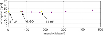
Figure 6. Optical absorption of one position of the AlGaAs coating for different laser light intensity: a beam radius of 35 μm was used for all measurements while the laser power was increased from 300 to 1760 mW. The measured absorption is shown by the purple squares, the yellow stars show the design intensity within the arm cavities for ET and aLIGO.
Download figure:
Standard image High-resolution image2.5. Comparison to HR coating
The AlGaAs coating stack is optimized for high reflectivity at 1064 nm while at 1530 nm we measured a transmission of approximately 70%.
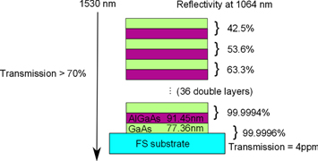
The coating is composed of alternating layers of GaAs and AlGaAs each with an optical thickness of a quarter of the wavelength of  . With refractive indices of
  and
and  at 1064 nm the optimal layer thickness would be 76.4 nm for GaAs and 89.3 nm for AlGaAs. The actual as-grown thicknesses of the layers are 77.36 nm for GaAs and 91.45 nm for AlGaAs.
At each layer boundary due to the change of refractive index light is reflected following Fresnel's formulas [28]. To calculate the actual reflectivity and laser power within each double layer of the coating stack, the coating stack was simulated using ray-transfer matrix formalism for calculating a series of reflecting boundaries. Details can be found in [29].
The resulting reflectance of the coating stack per double layer shows that at 1064 nm 42.5% of the input power is already reflected at the first double layer, 53.6% at the second double layer etc as indicated in figure 7. So the power within the first double layer is reduced to (100 − 42.5)%. The sum of the power per double layer results in an effective penetration depth of  double layers of the input laser power into the coating stack. The total absorption measured would thus be equivalent to the absorption from 2.6 double layers which saw the full power of the laser. Repeating this calculation for a wavelength of 1530 nm results in
  double layers.
Figure 7. Schematic of the AlGaAs coating stack: the coating is bonded to a FS disc. The stack consists of 81 quarter wave layers of alternating GaAs/AlGaAs starting and ending with GaAs. The calculated reflectivity per double layer at 1064 nm is given for the first three double layers showing that only a small part of the light propagates into the lower layers while at 1530 nm a transmission of  was measured.
Download figure:
Standard image High-resolution image
The ratio  gives the scaling which is required to make the measured absorption comparable to the expected absorption for a stack designed to be highly reflective at 1530 nm with the additional consideration that the quarter wave single layers will be thicker by
  . Scaling the measurement using these factors results in
  which is in good agreement with previous results at 1064 and 1550 nm [30].
3. Discussion and conclusion
We have used photo-thermal common-path interferometry to measure the optical absorption at 1530 nm of an AlGaAs crystalline coating stack, designed for high reflectivity at 1064 nm and bonded to a FS disk.
The AlGaAs coating bonded to FS showed an unexpectedly large signal originating directly from the coating, requiring the simulation and analysis of the signal to be adapted.
To check the uniformity of the coating, an area of 4 mm × 5.7 mm was mapped. The absorption of the complete stack as would be seen by the laser beam in a GW detector when transmitting the ITM was measured to be  . This includes substrate surface absorption and a possible absorption of the bond in between substrate and coating. Subtracting the lower limit for the substrate surface absorption,
  forms an upper limit for the coating absorption. The corresponding absorption coefficient is
  (
( ). This is equivalent to an absorption of
  in an AlGaAs stack designed for HR at 1530 nm. This is a very promising low absorption result for alternative low-loss coating materials. Still, further work will be necessary to reach the requirements of
  ppm for future GW detectors.
Measurements of the phase show evidence of non-uniformity in the thermal contact between the coating and the substrate, which may indicate variations in the quality of the bond. These may be related to a insufficient quality of the substrate polish. The surface of the FS disk to which the coating was attached showed an increased absorption compared to the back surface of the sample. This is unexplained, but may be related to the plasma cleaning procedure used prior to bonding the coating.
One possible source of the measured AlGaAs absorption could be contaminants from the MBE growth process, which was carried out in a chamber used to deposit various materials including doped semiconductor layers. A dedicated AlGaAs MBE system, with reduced potential for contamination, may enable higher purity, and thus possibly lower absorption, coatings to be produced.
Acknowledgments
G C acknowledges support from EURAMET/EMRP (QESOCAS) and thanks M Aspelmeyer from the University of Vienna for enlightening discussions. Mirror microfabrication was carried out at the Center for Micro- and Nanostructures (ZMNS) of the Vienna University of Technology. This work was partly funded by a Royal Society Research Grant (RG110331), and we are grateful for additional financial support from STFC (ST/L000946/1) and the University of Glasgow. IWM is supported by a Royal Society Research Fellowship. SR holds a Royal Society Wolfson Research Merit award. We are grateful to the International Max Planck Partnership for Measurement and Observation at the Quantum Limit for support, and we thank our colleagues in the LSC and VIRGO collaborations and within SUPA for their interest in this work. We thank Alexei Alexandrovski for valuable discussions. We would like to thank Riccardo Bassiri for attendance and valuable support during the most intense phase of preparing this manuscript and in particular for advising the most appropriate working environment including indispensable facilities and supplies. This paper has LIGO Document number LIGO-P1400226.