
Abstract
SnO2 films exhibit significant potential as cost-effective and high electron mobility substitutes for In2O3 films. In this study, Li is incorporated into the interstitial site of the SnO2 lattice resulting in an exceptionally low resistivity of 2.028 × 10⁻³ Ω⋅cm along with a high carrier concentration of 1.398 × 1020 cm−3 and carrier mobility of 22.02 cm2/V⋅s. Intriguingly, Lii readily forms in amorphous structures but faces challenges in crystalline formations. Furthermore, it has been experimentally confirmed that Lii acts as a shallow donor in SnO2 with an ionization energy ΔED1 of −0.4 eV, indicating spontaneous occurrence of Lii ionization.
Export citation and abstract BibTeX RIS
Currently, transparent conductive oxide (TCO) films prepared below 200 °C received increased attention due to the widespread application of temperature sensitive component in some devices, such as amorphous hydrogenated silicon in Si-heterojunction solar cells or polyvinyl alcohol in flexible optoelectronic devices.[1–6] Indium oxide (In2O3), tin dioxide (SnO2), and zinc oxide (ZnO) films are promising and technologically important TCO films in these applications. Wherein, indium tin oxide (ITO) films have been preferred in industry because of its excellent optical and electrical properties. However, the fact that indium is rare on earth limits its further applications. In addition, although doped ZnO films also presents excellent performance, they are also excluded from the options due to their poor chemical stability,[7] which greatly increases the difficulty of device encapsulation. Therefore, increasing attention is paid to SnO2, especially the F-doped SnO2 (FTO) films with outstanding optical and electrical performance, low cost, and chemical and environmental stability.
Among various preparation techniques, magnetron sputtering is expected to be the most suitable for depositing high-quality, well-adhered, and large-sized films at relatively low substrate temperature.[8] For instance, Morá n-Pedroso et al. reported FTO films deposited at room temperature by sputtering in an atmosphere containing H2 with optimized sheet resistance of ∼ 20 Ω/□.[9] Zhu et al.[10] obtained minimum resistivity of 8.5 × 10⁻³ Ω⋅cm for FTO films prepared at 150 °C and 300 °C. Wu et al.[11] obtained an FTO film with low resistivity of 5.4 × 10⁻³ Ω⋅cm.
In order to further enhance the optical and electrical performance of SnO2 films, it is imperative to explore donor impurities in SnO2 that are shallower than FO. This study reveals that Li, with a smaller radius, when incorporated into the interstitial site of amorphous SnO2 film, exhibits excellent donor characteristics despite being traditionally considered as an acceptor in crystalline SnO2.[12] The LiTO films were prepared at 180 °C by magnetron sputtering using a Li0.01Sn0.99O2 target in an Ar + O2 atmosphere to investigate the behavior of Li doping in SnO2 as well as the optical and electrical properties of the resulting LiTO film. Remarkably, we achieved simultaneous enhancements in carrier concentration n (1.398 × 1020 cm−3), mobility μ (22.02 cm2/V⋅s), and resistivity ρ (2.028 × 10⁻³ Ω⋅cm) on the LiTO film. Interestingly, we observed that Lii formation and consequently electrical performance are significantly influenced by the crystallinity of LiTO films. Specifically, Lii is more likely to form in amorphous structures but less likely to form in crystalline ones. Consequently, amorphous films consistently exhibit superior electrical performance compared to their crystalline counterparts. Furthermore, we have confirmed that Lii acts as a shallow donor impurity within SnO2 with an ionization energy ΔED1 of −0.4 eV, indicating spontaneous occurrence of Lii ionization.
LiTO films were fabricated on quartz glass substrates at 180 °C by magnetron sputtering using Li0.01Sn0.99O2 targets. LiTO films with different thicknesses were prepared at different deposition times of 28, 42, and 70 min, named as LiTO1, LiTO2, and LiTO3, respectively. In addition, a SnO2 film was prepared for comparison using a SnO2 target. The diameters of the targets were two inches. The bare pressure of the sputtering chamber was 1.2 × 10⁻⁴ Pa and the sputtering was performed at 0.4 Pa under a mixed atmosphere of Ar (99.1%) and O2 (0.9%). All the targets were powered at 30 W and placed 10 cm away from the substrates. The quartz glass substrates were ultrasonically cleaned in acetone, alcohol, and deionized water for 15 min in sequence, and the targets were pre-sputtered for 5 min to remove any contaminant from the target surface before films deposited on the substrates. The substrate temperature was set to 180 °C during film growth.
Composition of films were measured by x-ray photoelectron spectroscopy (XPS). The crystal structure of films was characterized by x-ray diffraction (XRD). Thickness and surface morphology of thin films were determined by an atomic force microscope. An infrared (UV-vis-NIR) spectrophotometer was used to measure the optical properties, and Hall measurements (Ecopia HMS-3000) were performed to test resistivity, carrier concentration, and mobility of films. Ultraviolet photoelectron spectra (UPS) were performed to characterize Fermi level and valance band of selected thin films.
To understand the chemical bonding state of the films, the typical core level XPS spectra are shown in Figs. 1 and 2. All the bonding energies are corrected based on 284.8 eV of C 1s. Figure 1 shows a broad asymmetric curve of O 1s spectrum, which was fitted by two peaks for the SnO2 film with binding energies centered at 530.37 eV and 531.8 eV typically ascribed to O–Sn4+ and O chemically adsorbed on the surface, respectively.[13,14] A new peak centered at 530.15 eV must be deconvoluted to fit convergence for LiTO films as shown in Fig. 2(a), which can be attributed to Sn–O–Sn in the vicinity of interstitial Li (Lii ). The binding energy decrease can be attributed to both attraction between Li and O and repulsion between Li and Sn. Furthermore, the peak intensity decreases significantly, indicating Lii content decreasing. Moreover, in the Li 1s spectrum shown in Figs. 2(b), 2(c), and 2(d), interestingly, there is no signal at all in this region for LiTO films, meaning that Lii in SnO2 is hard to be detected with the XPS spectrum. Therefore, assuming that Li only has a profound impact on the bond energy of the nearest Sn–O–Sn bond, the content of Li can be estimated based on the area of the 530.15 eV peak and the results are summarized in Table 1.
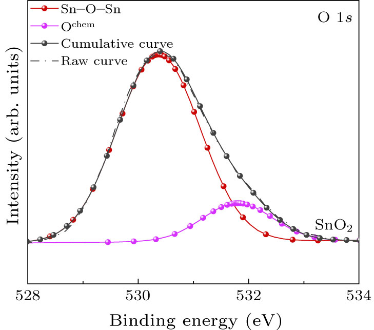
Fig. 1. XPS spectra in the O 1s region for SnO2 films.
Download figure:
Standard image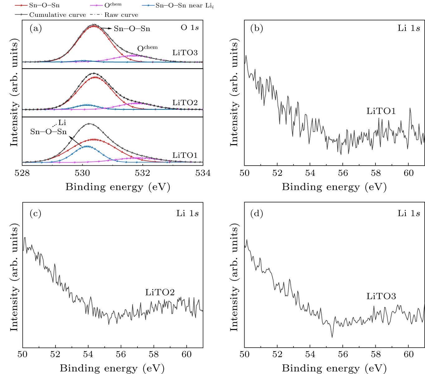
Fig. 2. (a) XPS spectra in the O 1s region for LiTO films and Li 1s region for (b) LiTO1, (c) LiTO2, and (d) LiTO3 films.
Download figure:
Standard imageTable 1. The element content measured by XPS, thickness, and roughness for SnO2 and LiTO films. Rq: the root mean square value of sample surface height within the testing area.
| Film | Chemical composition (at.%) | Thickness (nm) | Rq (nm) | |||
|---|---|---|---|---|---|---|
| Sn | O | Li | O/Sn | |||
| SnO2 | 34.54 | 65.46 | – | 1.90 | 77 | 0.673 |
| LiTO1 | 31.83 | 65.03 | 3.14 | 2.04 | 50 | 0.509 |
| LiTO2 | 34.54 | 64.57 | 0.89 | 1.87 | 90 | 0.526 |
| LiTO3 | 35.32 | 64.47 | 0.21 | 1.83 | 150 | 0.575 |
Table 1 shows the element composition for SnO2 and LiTO films. From the table, the content of Li in LiTO1 film is 3.14 at.%, which significantly decreases to 0.89 at.% of LiTO2 and 0.21 at.% of LiTO3. In addition, although O2 was added during film growing, the O/Sn atomic ratio of SnO2 is 1.90 ascribed to ion bombardment. The ratio is 2.04 for LiTO1, which indicates fewer oxygen vacancies (VO). Surprisingly, the ratio decreases to 1.87 of LiTO2 and 1.83 of LiTO3 as Lii content decreases, which can be attributed to their lager deposition rate (2.17 nm/min of LiTO2 and 2.19 nm/min of LiTO3) compared to 1.75 nm/min of SnO2 and 1.79 nm/min of LiTO1, leading to less time to be oxidized by additional O2 in the deposition chamber. Furthermore, the large O/Sn ratio difference between SnO2 and LiTO1 films under similar deposition rates can be attributed to the presence of Lii in SnO2, which inhibits the formation of VO.
Figure 3 presents the x-ray diffraction patterns of all films over the 2θ, ranging from 5° to 90°. It can be seen that SnO2 film presents an amorphous structure. In addition, LiTO1 is also amorphous due to its thin thickness. Expectedly, (200) and (211) peaks located at 37.9° and 51.8° (PDF card: No. 41–1445), respectively, appear for LiTO2, and intensity of the two peaks further increases along with the appearance of another (110) peak centered at 33.9° (PDF card: No. 41–1445) for LiTO3, which means that the crystallinity of the films increases as the film thickness increases. Moreover, Li compounds are doped into host SnO2 lattice or amorphous since no other diffraction peaks can be detected. Surprisingly, there is a strong correlation between the Lii content and the crystallinity. Specifically, the lower the crystallinity, the higher the Lii content in the film. In the amorphous state, only the first-shell corresponds to the nearest Sn–O bonds. In a longer range, all structural features are suppressed, and thus the amorphous structure of SnO2 can be regarded as a random combination of nearest neighbor Sn–O structures. These combinations, like In2O3, are also composed of face-shared, edge-shared, corner-shared, and non-shared types.[15] The combinations of corner-shared and non-shared types will produce some large-sized interstitial sites, leading to easier formation of Lii . However, for SnO2 with a crystalline rutile structure, even the size of the largest octahedral interstitial site of 72 pm is smaller than the diameter of Li+ (120 pm), making it difficult to form Lii . Therefore, the low crystallinity of LiTO with high Li content can be attributed to the lower formation energy of Lii in amorphous crystals. In addition, the interaction between Lii and its nearest neighboring Sn–O bonding will further reduce the formation energy of Lii and improve its stability.

Fig. 3. The XRD patterns of SnO2 and LiTO films.
Download figure:
Standard imageFurthermore, to investigate electrical performance evolution, carrier concentration n, mobility μ, and resistivity ρ of SnO2 and LiTO films are measured and summarized in Table 2. The SnO2 film is almost insulated and its resistivity exceeds the range of the Hall measurement. Surprisingly, LiTO1 film exhibits an extremely low resistivity of 2.028 × 10⁻³ Ω⋅cm and high μ of 22.02 cm2/V⋅s. This high mobility can be ascribed to its insensitiveness to the distorted Sn–O–Sn chemical bonds originated from the magnitude of isotropic neighbouring Sn 5s orbitals overlap.[16] Due to few VO in the film suggested by the high O/Sn ratio as shown in Table 1, it can be rationally concluded that Lii with very small activation energy mainly causes the conductivity of the film. Moreover, resistivity ρ increases to 5.548 × 10⁻³ Ω⋅cm for LiTO2 and further increases to 17.780 × 10⁻³ Ω⋅cm for LiTO3 with reduced Lii content. It is worth noting that the film mobility continues to decrease with the optimization of film crystallinity. As for LiTO2 film, due to the coexistence of (200) oriented crystalline grains and amorphous phases, electrons are subject to interface scattering during transport between amorphous and crystalline grains, resulting in a decrease in electron mobility to 17.42 cm2/V⋅s. Furthermore, when electrons are transported between amorphous phase and crystalline grains, as well as crystal grains with different orientations, they are subjected to significant interface scattering effects, resulting in a further decrease in the electron mobility to 11.43 cm2/V⋅s of LiTO3 film. In addition, compared with ITO films prepared under the similar conditions with resistivity of about 2 × 10⁻³ Ω⋅cm,[17] LiTO films exhibit competitive electrical resistivity and even higher carrier concentration, which suggests that it is entirely possible for LiTO films to replace expensive ITO films in low-temperature applications, especially under conditions below 200 °C.
Table 2. The electrical and optical performance of SnO2 and LiTO films measured at 25 °C.
| Film | n (1020/cm3) | μ (cm2/V⋅s) | ρ (10−3Ω⋅cm) |
 (× 10−4 nm−1) (× 10−4 nm−1) | Eg (eV) |
|---|---|---|---|---|---|
| SnO2 | – | – | – | 2.39 | 3.45 |
| LiTO1 | 1.398 | 22.02 | 2.028 | 5.46 | 3.63 |
| LiTO2 | 0.646 | 17.42 | 5.548 | 2.36 | 3.74 |
| LiTO3 | 0.307 | 11.43 | 17.780 | 1.97 | 3.81 |
In addition, the optical absorption coefficients α of SnO2 and LiTO films as a function of wavelength are shown in Fig. 4(a) to eliminate the influence of film thickness for better optical performance comparison. Meanwhile, the mean absorption coefficient  are calculated by[18]
where Γ (λ) and S(λ) represent the standard AM1.5 solar photon spectral distribution and the experimental absorption coefficient as shown in Fig. 4(a). The calculation results are summarized in Table 2. The absorption coefficient of SnO2 sample is quite low, and the average absorption coefficient is 2.39 × 10⁻⁴ nm−1. For LiTO1 film, a high  of 5.46 × 10⁻⁴ nm−1 as a result of the plasmon absorption caused by high carrier concentration is presented. Furthermore, as the thickness of the film increases, the Lii
content in the film decreases, and thus the carrier concentration decreases, resulting in a decrease of absorption as shown in Fig. 4(a) and decline of
of 5.46 × 10⁻⁴ nm−1 as a result of the plasmon absorption caused by high carrier concentration is presented. Furthermore, as the thickness of the film increases, the Lii
content in the film decreases, and thus the carrier concentration decreases, resulting in a decrease of absorption as shown in Fig. 4(a) and decline of  to 2.36 × 10⁻⁴ nm−1 for LiTO2 and 1.97 × 10⁻⁴ nm−1 for LiTO3. Moreover, the change in photon energy hν and optical absorption coefficient (α) for the SnO2 and LiTO films are displayed in Fig. 4(b) to extract optical band gap according to the following relation:[18] (αhν)2 = A(hν–Eg), where A is a constant. The extracted optical band gap is summarized in Table 2. The Eg of SnO2 is 3.45 eV, which is smaller than reported 3.6 eV[19] attributed to numerous VO. For the LiTO films, the Burstein–Moss effect, lattice distortion caused by interstitial Li doping, film thickness, and crystallinity would have a profound impact on the bandgap of the films.[20,21] The ΔEg, BM resulted from the Burstein–Moss effect can be calculated by the following relationship:[21]
where h is Planck's constant, m* is the reduced effective mass that is 0.3m0 for SnO2. In addition, the crystallinity of the films can be evaluated using the grain size calculated by the Debye–Scherrer formula[22] utilizing full width at half maximum of XRD diffraction peaks, and the estimated grain sizes of LiTO2 and LiTO3 are 14.9 nm and 22.4 nm, respectively.

Fig. 4. (a) Optical absorption coefficient and (b) optical band gap of SnO2 and LiTO films.
Download figure:
Standard imageConsidering that the SnO2 and LiTO1 films are both amorphous, the influence of crystallinity on the band gap can be supposed to be the same. Meanwhile, the calculated ΔEg, BM of LiTO1 is 0.33 eV and a bandgap reduction of ∼ 0.1 eV due to the small thickness in comparison with SnO2 film based on Ref. [20]. Therefore, the band gap reduction resulting from lattice distortion caused by interstitial Li doping is estimated to be 0.05 eV, which is not obvious. It can be reasonably ignored in the case of LiTO2 and LiTO3 films with much low Li content. Furthermore, the calculated ΔEg, BM values for LiTO2 and LiTO3 are 0.2 eV and 0.12 eV, respectively. When the thickness of the film exceeds 79 nm, the influence of film thickness on the bandgap of the film is significantly reduced and the thicker thickness only increases the bandgaps of LiTO2 and LiTO3 films by approximately 0.01 eV and 0.04 eV, respectively, compared to SnO2 based on Ref. [20]. Therefore, the significant optimization of the crystallinity of the film at this time plays a major role in bandgap increasement of the both films. Finally, the crystalline effects for LiTO2 and LiTO3 films are estimated to be 0.08 eV and 0.2 eV, respectively.
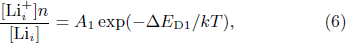
The resistance of LiTO1 film in the temperature range 1.9–400 K are shown in Fig. 5. The film resistance varies with temperature in three stages: The characteristic of stage I is that the resistance decreases with increasing temperature. This can be ascribed to that as the temperature increases, the Lii donor impurity is excited, the carrier concentration increases, and the mobility is controlled by ionized impurity scattering, which also increases with increasing temperature. It is not until 89 K that the donor impurity is fully excited, and the mobility is equivalent to lattice vibration scattering by ionized impurity scattering. In stage II, the donor impurity is fully excited and the mobility changes from dominated by ionized impurity scattering to dominated by lattice vibration scattering. As the temperature increases, the mobility decreases and the resistance increases until 371 K, and the intrinsic excitation effect becomes apparent. The intrinsic excitation mechanism in stage III is dominant, and as the temperature increases, the carrier concentration increases and the resistance decreases.

Fig. 5. (a) Resistance variation with temperature and (b) plot of ln(σT3/2) versus 1000/T of LiTO1 film.
Download figure:
Standard imageFurthermore, the defects in the LiTO1 film are Lii and VO. Therefore, the ionization reaction of these defects can be written in the following form:


According to the mass action equilibrium formulas, they have the following relationship:
Here, n is also the carrier concentration. ![$[{{\rm{Li}}}_{i}^{+}]$](https://content.cld.iop.org/journals/0256-307X/41/3/037305/revision2/cpl_41_3_037305_ieqn5.gif) ,
, ![$[{V}_{{\rm{O}}}^{+}]$](https://content.cld.iop.org/journals/0256-307X/41/3/037305/revision2/cpl_41_3_037305_ieqn6.gif) , and
, and ![$[{V}_{{\rm{O}}}^{++}]$](https://content.cld.iop.org/journals/0256-307X/41/3/037305/revision2/cpl_41_3_037305_ieqn7.gif) are the ionized defect concentrations. [Lii
] and [VO] are the concentrations of Lii
and VO, respectively. ΔED1, ΔED2, and ΔED3 are ionization energies of relevant reactions. A1, A2, and A3 are pre-exponentials of the reactions. On this basis, according to Ref. [23], the conductivities of LiTO1 film are given as
are the ionized defect concentrations. [Lii
] and [VO] are the concentrations of Lii
and VO, respectively. ΔED1, ΔED2, and ΔED3 are ionization energies of relevant reactions. A1, A2, and A3 are pre-exponentials of the reactions. On this basis, according to Ref. [23], the conductivities of LiTO1 film are given as
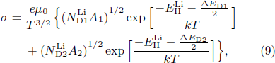
where  and
and  represent the concentrations of doped Li and singly ionized oxygen vacancy, respectively; k is Boltzmann's constant; μ0 is another pre-exponential factor.
  is the electron hopping energy, which is 0.242 eV reported in Ref. [23]. In this work, it can be determined that there is almost no VO in the LiTO1 film from the O/Sn ration of 2.04, and high concentration of electrons from the ionization of Lii
can further suppress reactions (4) and (5), which leads to a negligible
is the electron hopping energy, which is 0.242 eV reported in Ref. [23]. In this work, it can be determined that there is almost no VO in the LiTO1 film from the O/Sn ration of 2.04, and high concentration of electrons from the ionization of Lii
can further suppress reactions (4) and (5), which leads to a negligible  . Therefore, there exists the following relationship for LiTO1 film:

The ionization energy ΔED1 of Lii can be determined from ln (σT3/2) plot versus 1000/T, as shown in Fig. 5(b). The slope of the straight line in the figure is −0.49, deducing a ΔED1 of −0.4 eV, which is less than 0, meaning that Lii ionization always occurs spontaneously.
To further illustrate the physical mechanisms of optical and electrical performance evolution, energy levels of LiTO films are investigated using UPS. Figure 6 shows the secondary electron cutoff region representative for the WF and the valance band (VB) edges of LiTO films. The exact VB offset is determined by extrapolating the leading edge of the VB spectrum to the base line. The WF of LiTO1 (WF = −3.58 eV) slightly shifted toward a higher energy by 0.34 eV as compared to LiTO2 (WF = −3.92 eV), and 0.46 eV as compared to LiTO3 (WF = −4.04 eV), which conforms well the carrier concentration n. Also, based on the UPS spectra and the optical bandgap Eg shown in Table 2, the relevant energy band structure diagrams are constructed in Fig. 6(d).
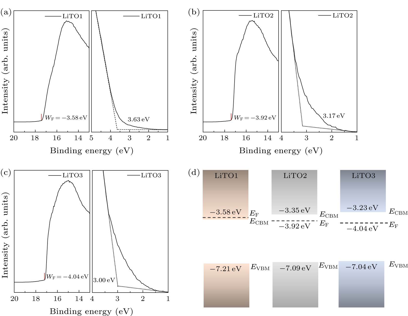
Fig. 6. UPS spectra of (a) LiTO1, (b) LiTO2, and (c) LiTO3 films, and (d) energy band structure diagrams of LiTO1, LiTO2, and LiTO3 films.
Download figure:
Standard imageIn summary, we have investigated the structure and properties of low-temperature sputtered LiTO films. Two significant conclusions can be proposed: (i) Lii tends to form easily in amorphous structures but faces difficulties in crystalline formations. (ii) Lii acts as a shallow donor in SnO2, with an estimated ionization energy ΔED1 of −0.4 eV, indicating spontaneous occurrence of Lii ionization. Consequently, the LiTO film simultaneously achieves excellent resistivity of 2.028 × 10⁻³ Ω⋅cm, accompanied by high carrier concentration of 1.398 × 1020 cm−3 and carrier mobility of 22.02 cm2/V⋅s. The present study is expected to contribute significantly to the advancement of low-temperature magnetron sputtering for the growth of doped SnO2 transparent conductive films, thereby yielding substantial benefits in their applications.
Acknowledgments
This work was supported by the Key-Area Research and Development Program of Guangdong Province (Grant No. 2021B0101260001), the Guangdong Basic and Applied Basic Research Foundation (Grant No. 2019A1515110411), and partly the INTPART Program at the Research Council of Norway (Grant No. 322382).