

Abstract
Surface plasmons confining strong electromagnetic fields near metal surfaces, well-known as hot spots, provide an extremely efficient platform for surface-enhanced Raman scattering (SERS). In this work, SERS spectra of probing molecules in a silver particle–wire 1D nanostructure on a thin gold film are investigated. The Raman features of SERS spectra collected at the particle–wire joints exhibit an obvious wavelength dependence phenomenon. This result is confirmed electromagnetic field simulation, revealing that hot spot distribution is sensitively influenced by the wavelength of incident light at the joints. Further studies indicate this wavelength dependence of hot spot distribution is immune to influence from the geometric shape of the particle or the angle between wire and particle, which improves fabrication tolerance. This technology may have promising applications in surface plasmon related fields, such as ultrasensors, solar energy and selective surface catalysis.
Export citation and abstract BibTeX RIS
1. Introduction
Surface plasmon polaritons (SPPs)—collective electromagnetic excitations combined with coherent oscillation of electrons near the interface between dielectric media and metal conductors—interact strongly with incident electromagnetic (EM) waves and can be evanescently confined to the surfaces with subwavelength attenuation length [1–4]. Associated with noble metal nanostructures, these resonances possess sharp spectral absorptions and scattering peaks as well as several-order-of-magnitude enhancement of electromagnetic field near the interface at visible and near-infrared wavelengths. A class of non-propagating SPPs stemming from the strong coupling between metallic nanostructures and EM field are called localized surface plasmons (LSPs). On the strength of these remarkable merits, many marvellous phenomena associated with SPPs and LSPs have been discovered and have led to further development in several areas of science and technology, such as molecular detection [5], nonlinear plasmonics [6], extraordinary optical transmission [7], optical trapping [8], waveguiding beyond diffraction limits [9], optical thermal effects [10], solar cells [11], optical activity [12], etc.
Surface-enhanced Raman scattering (SERS) is a useful technique which possesses extremely large Raman cross sections, benefiting from ultrahigh energy density of light and chemical enhancement, where the latter factor primarily originates from the charge transfer mechanism, and could even achieve the detection of a single molecule or an extremely small nanoparticle [5, 13–17]. The large enhancement of Raman signals in SERS could reach factors of 1010–1011; it has been widely used in various scientific areas including environmental analysis [18], surface catalysis [19], cancer detection [20], forensic science [21], archeological research [22] etc. Due to localized surface plasmon resonance (LSPR) in metallic nanostructures, SERS in the enhanced optical fields arises prolifically, resulting in the electromagnetic enhancement being approximately equal to  .
.
As we all know, the crucial factor in SERS is the configuration of metal nanostructures. The most common SERS structures always contain sharp corners or nanogaps between nanoparticles and thin films, known as hot spots, with high EM energy density, so that the prominent field enhancement at these positions can make great contributions to enhancement of the Raman cross section [2, 23]. Besides, excitation sources, substrate, the surrounding medium and other factors will also influence the generation of hot spots in SERS [24]. Recent researches related to the nanoparticle-film assisted SERS system have reported an interesting surface plasmon related phenomenon: that the hot spots could be transferred between different gaps by changing the wavelength of incident light [16, 17, 25–27]. This wavelength modulated hot spots distribution phenomenon greatly promotes the potential applications of SERS, such as selective SERS detection in complex nanostructure, 2D materials SERS detection. Compared to nanoparticle aggregation, 1D metal nanostructures such as particle–wire nanostructures provide a straightforward way to determine the most efficient polarization direction, which is crucial in the surface plasmon related phenomenon [28–31]. Therefore, the investigation of wavelength modulated hot spot distribution in 1D nanostructures on metal film is a charming area with great potential application.
In this paper, a 1D nanostructure composed of silver particle–wire on a thin gold film is realized. The detecting molecules are benzene-1,4-dithiol (BDT) and 2-amino-5-nitrobenzenethiol (2A-5NBT); one coats the silver particle–wire and the other is located at the surface of the gold film. Raman scattering spectra are collected at different illuminating positions, and two typical laser wavelengths (532 nm and 633 nm) are used to study the frequency influence of the hot spot locations. The experimental results indicate that the distribution of hot spots at 532 nm excitation is tightly confined to the gap between nanoparticle and nanowire, while at 633 nm excitation the distribution is confined not only to this gap but also the gap between the nanoaggregate and film. The electric field enhancement is also clearly demonstrated through numerical simulation and shows good agreement with the experimental results. We have also taken the geometric shape of nanoparticles and the inclined angle between the nanoparticle and nanowire into consideration—we found their influence on the system to be negligible.
2. Experimental section
2.1. Materials
Silver nitrate (AgNO3), Polyvinylpyrrolidone (PVP K30) and ethylene glycol (EG) were purchased from Aladdin. 2-amino-5-nitrobenzenethiol (2A-5NBT) and benzene-1,4-dithiol (BDT) were purchased from Aldrich Chemical Co. The Au film (thickness about 100 nm) was prepared by vacuum evaporation coating onto the silicon substrate under high vacuum environment using electron beam evaporation. The root mean squared surface roughness of the resulting Au film was measured to be 2.249 by atomic force microscopy (AFM), which is smooth enough for current experimental requirements.
2.2. Synthesis of silver nanoparticles and nanowires
Uniform, monocrystalline silver nanoparticles and nanowires were simultaneously synthesized by the polyol method [32]. PVP and AgNO3 solutions were added into heated EG, stirring at 160 °C for about one hour and rinsed with ethanol. Scanning electron microscope (SEM) images of these samples indicate that both the nanoparticles and nanowires were synthesized well enough, with quite smooth surfaces at the same time.
2.3. Raman spectroscopy measurements
A clean Au film was immersed in 0.5 mM BDT solution for 2.5 h, then rinsed with ethanol. Meanwhile, the colloidal solution containing Ag particle and wire nanostructures was added into 0.5 mM 2A-5NBT solution and stirred by a magnetic rotor for 2.5 h, then rinsed in a centrifuge with ethanol. After that, 2A-5NBT and BDT molecules were coated onto the surface of the silver nanostructures and Au film respectively. The colloidal solution was well distributed on the Au film through spin-coating. The sample was maintained at room temperature until dry; a schematic diagram of the sample is shown in figure 1(a). The Raman spectra of the two molecule powders are presented in figures 1(b) and (c). The other sample in our work including 2A-5NBT covered Au film and BDT-covered Ag particle–wire nanostructure was prepared in a similar way by replacing the BDT (2A-5NBT) by 2A-5NBT (BDT) molecules in the steps described above.
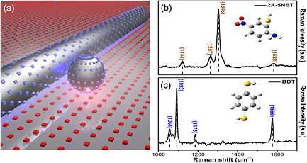
Figure 1. (a) Schematic diagram of the sample setup, single-layer BDT molecules (red dots) are adsorbed onto Au film and 2A-5NBT molecules (blue dots) are adsorbed onto the surfaces of particle–wire nanostructures. (b) and (c) Raman spectra of the pure powder of the two probing molecules, 2A-5NBT and BDT, respectively.
Download figure:
Standard image High-resolution imageAll of the SERS experiments in this work were measured by a commercial Micro-Raman spectrometer (Horibba). Lasers with two wavelengths (532 nm and 633 nm) were chosen to be the illuminating sources, and the electric field polarization direction was set up to be perpendicular to the nanowires in order to obtain the maximum electric field enhancement [33]. The morphology and sizes of the silver nanostructures were characterized by scanning electron microscopy (SEM).
3. Numerical simulation
The near-field electric field distributions were simulated with a finite element method (FEM) using COMSOL Multiphysics. Perfectly matched layer (PML) boundary conditions were adopted for all side walls, and realistic parameters of permittivity and permeability were used in the simulations for gold and silver [34]. The thickness of the Au film was 100 nm, and the sizes of all edge-to-edge gaps of nanostructures were set to 1 nm to accommodate the thickness of two single covering layers of probing molecules, each of which being about 0.5 nm thick. Plane waves with a fixed wavelength (532 nm and 633 nm) are used as an incident source, which propagates normally toward the gold film from the particle–wire side; the convergence of the numerical results is checked by altering the mesh size.
4. Results and discussion
SEM images of Ag 1D particle–wire nanostructures on Au film are shown in the insets of figures 2(a) and (b)—they show the morphology and geometric scale of the sample, so that the approximate structural parameters can be read out. Doing so, the nanoparticle here is a nanocube with the edge length measured to be about 650 nm; the diameter of the nanowire is measured to be about 700 nm and its length 8.31 µm. The yellow dashed circles in the insets of figures 2(a) and (b) show the catchment areas of corresponding SERS experiments. The polarization of the incident laser beam is always chosen to be perpendicular to the nanowire.
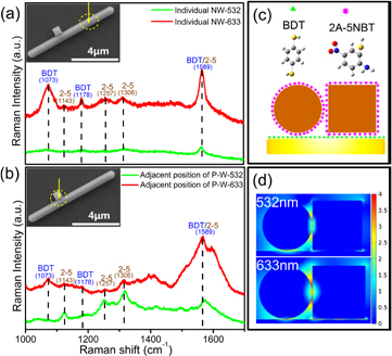
Figure 2. (a) and (b) Raman spectra for different positions (yellow dashed circle area in the insets). The incident laser beam (two typical wavelengths 532 nm and 633 nm, respectively) illuminates normally to the sample plane, with its polarization perpendicular to the nanowire. The yellow dashed circle areas in the insets represent the laser facula; its diameter is about 2–3 µm. (c) Scheme of the detected sample with BDT molecules adsorbed on the Au film and 2A-5NBT molecules adsorbed on the surfaces of Ag particle–wire nanostructure. (d) Simulation results of the system at the position of figure (b) excited at 532 nm and 633 nm respectively. The edge length of the nanocube is about 650 nm and the diameter of the nanowire is about 700 nm.
Download figure:
Standard image High-resolution imageDue to the precision of the Raman spectrometer, the peaks at 1064 and 1093 cm−1 of BDT merge together at 1073 cm−1 in our experiment. Figure 2(c) shows the scheme of the sample with BDT molecules adsorbed onto the Au film and 2A-5NBT molecules adsorbed onto the surface of a particle–wire nanostructure. As shown in figures 2(a) and (b) respectively, the SERS spectra were collected at a specific location on a single nanowire and the adjacent position of the particle–wire nanostructure. The Raman spectra collected at the specific nanowire location are similar for 532 nm (green line) and 633 nm (red line) excitation are shown in figure 2(a). They both exhibited the Raman feature of BDT probing molecules with peaks at 1073, 1178 and 1589 cm−1, and 2A-5NBT molecules peaks at 1143, 1257, 1306 and 1589 cm−1. The much smaller intensities excited by 532 nm laser in SERS spectra come from 3d electron transitions under high energy conditions. It should be noted that the Raman spectra we obtained are the superposition of signals from two different probing molecules. For Raman signals from the adjacent position of particle–wire nanostructure shown in figure 2(b), the Raman signal enhancement of BDT and 2A-5NBT molecules are obviously the same as the 633 nm excitation, while only the enhancement of 2A-5NBT molecules could be found at 532 nm excitation. This could be distinguished by the sharp peaks of BDT and 2A-5NBT molecules at 633 nm, and only sharp peak of 2A-5NBT molecules appears at 532 nm excitation. One should notice that the BDT molecules exist on the gold film and the 2A-5NBT molecules are adsorbed onto the surface of Ag nanostructure. This means that under 633 nm excitation the signal comes from the gaps of the silver particle–wire nanostructures and the gaps between them and the gold film, while the signal triggered by 532 nm excitation comes only from the gaps of the silver particle–wire nanostructures. The Raman signal, which primarily comes from the hot spots and differentiates under different laser sources, indicates that the distribution of hot spots is related to the excitation source. In order to illustrate our analysis further and understand the underlying mechanism, numerical simulations are performed by COMSOL. The 2D cross section view of the simulation results are shown in figure 2(d) for 532 nm and 633 nm. More specifically, the distribution of hot spots for 532 nm is mainly localized at the gap between the nanocube and the appressed nanowire, where the enhancement factor of electric field is approximately 95. However, the enhancement factor in the gap between the nanowire and the film is only about 8, and even 0 between the nanocube and the film. Conversely, for 633 nm excitation, the energy localizes not only at the gap between the nanocube and nanowire but also the gap between this nanoaggregate and the film. The enhancement factor of electric field is 76 at the gap of the nanoaggregate, 30 at the gap between the nanowire and Au film and 17 at the gap between the nanocube and the film. The simulation result verified our inference that the distribution of hot spots in the particle–wire nanostructure is related to the excitation source. The energy is closely confined at the gap between the nanoparticle and nanowire for 532 nm excitation.
The inclined angles between the nanocube and nanowire are also studied here to demonstrate the stability of this system. As shown in the SEM images in figure 3, the nanocube is tilted about 30°, and the geometric size is almost the same as that stated previously for the zero-angle tilt, so we can quantify the influence caused by the factor of inclined angles.
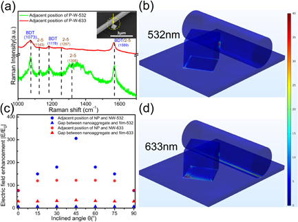
Figure 3. (a) Raman spectra at the position of the yellow dashed circle area of the inset; polarization of the laser is perpendicular to the nanowire, the incident laser beam is illuminating normally to the sample plane at 532 nm and 633 nm. The yellow dashed circle areas in the insets represent the laser facula, the size is about 2–3 µm. (b) and (d) Simulation results of the nanocube–nanowire–film SERS system at 532 nm and 633 nm respectively. Edge length of nanocube is about 650 nm and diameter of nanowire is about 700 nm. The inclined angle between nanocube and nanowire is about 30° and the rightmost color bar is normalized to the incident source with unit electric field. (c) COMSOL simulation results of enhancement of electric field at the gap between the nanocube and nanowire (dot) and the gap between the nanoaggregates and gold film (triangle) with different inclined angles, other parameters are chosen to be the same as in figure 2.
Download figure:
Standard image High-resolution imageFigure 3(a) shows the Raman spectra of the adjacent position of particle–wire nanostructure. The Raman intensity with 532 nm excitation is weaker than 633 nm excitation, this could be understood by 3d electron transitions at high light energy situations. In addition, the nonuniform distribution of the probing molecules may lead to a paucity of targets at the sharp corners of nanocubes, so that the Raman intensity is not too large. The SERS intensity of 2A-5NBT molecules at 532 nm excitation is more prominent than BDT molecules, while the distinction for 633 nm excitation is not obvious. This means that, different from the 633 nm situation, hot spots are mainly located at the gap of the nanoaggregate under 532 nm excitation. The simulation results further confirmed our inferences, as shown in figure 3(b). The rightmost color bar in figure 3(b) is normalized to the incident source with unit electric field.
The electric field enhancement at the gap between the nanoaggregate and the film is much stronger at 633 nm excitation than 532 nm. The enhancement factor with 532 nm excitation at the gap between nanoparticle and nanowire, the gap between nanoparticle and Au film, and the gap between nanowire and Au film are 78, 7 and 6 respectively, while they are 78, 78 and 30 for 633 nm excitation. To make the angle dependence more intuitive, we performed several simulations with different angles of inclination between the nanocube and nanowire from 0 to 90°. As shown in figure 3(c), the maximum field enhancement always located at the gap between the nanocube and nanowire while the amplitude increases with the angle and reaches an extremum at 45° for 532 nm excitation. It is quite clear that the contacting angle becomes sharpest at the 45°, so that the energy could be confined to the smallest region, thus leading to the largest electric field enhancement. However, the enhancement at the gap between the nanocube and nanowire for 633 nm excitation is not so sensitive—except the clingy case, the electric field enhancements tend to be constant across inclination angles. More importantly, the most remarkable difference is electric field enhancement in the gap between the nanoaggregate and the film—the enhancement factor is less than 10 for 532 nm excitation. Nevertheless, 633 nm excitation leads to a much larger enhancement factor (more than 30). It is clear that the hot spots are mostly located at the gap of particle–wire nanostructures and barely present at the gap between the nanoaggregate and film with 532 nm excitation. The promising part is the stability of the prominent feature of the distribution of hot spots (weakly dependent on the inclined angle) for 532 nm, which could greatly improve future prospects.
Based on the nanocube, which we proposed above could cause hot spot redistribution, various geometric shapes of nanoparticles are discussed in this particle–wire–film system. As shown in the insets of figure 4(a), a distorted nanopolyhedron is chosen as a sample to experimentally show the influence of the shape of nanoparticles. This time we also reverse the positions of two probing molecules to make sure of the target independence of the measurement. The scheme of the adsorbing molecules is shown in figure 4(b). Figure 4(a) shows the Raman spectra of the adjacent position of distorted nanopolyhedra and nanowire. However, the 2A-5NBT probing molecules show the same prominent Raman peaks with BDT molecules at 633 nm excitation, while only the characteristic peaks of BDT molecules could be seen under 532 nm laser excitation. This result confirmed the validity of our inference: the distribution of hot spots is tightly confined in the gap of nanoparticle and nanowire at 532 nm excitation, and does not dependent on the characteristics of the probing molecules. For this sample, there exists an additional Raman peak at 1415 cm−1—this could be explained by the Raman features of impurities introduced during sample preparation; we indeed identified the impurities here to be PVP molecules through checking the standard Raman spectrum of PVP. In general, the location of hot spots is very clear and the impurities have little influence on the Raman features of the two assigned probing molecules.
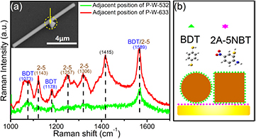
Figure 4. (a) Raman spectra at the position of yellow dashed circle area. The incident laser beam (532 nm and 633 nm respectively) illuminates normally to the sample plane; laser polarization is perpendicular to the nanowire and its diameter is about 500 nm. The yellow dashed circle area in the insets represents the laser facula, which is about 2–3 µm. (b) Scheme of the sample in (a) with 2A-5NBT molecules adsorbed on Au film and BDT molecules adsorbed on the surfaces of particle–wire nanostructure.
Download figure:
Standard image High-resolution imageOther regular geometric shapes of nanoparticles are also studied through numerical simulations. Some of them are difficult to synthesize in experiments. In order to show the weak sensitivity to the geometric size, the radius of the nanowire is reduced to 200 nm in the corresponding simulations and the nanowire is truncated to 4 µm for better views. Here we show the hot spot distribution of three typical nanoparticles (nanosphere, upright nanocylinder and nanotorus) with excitation wavelength at 532 nm (figures 5(a)–(c)) and 633 nm (see appendix). Without doubt, the enhancement of electric field is relatively weak at the individual nanowire part. As shown in figure 5, the hot spots at the adjacent part are mostly located in the gap between the nanoparticle (NP) and nanowire (NW), merely in the gap of the nanoaggregate and the film for all of the three cases. While at the adjacent positon, hot spots emerge at both the gap of nanoparticle and nanowire and the nanoaggregate and gold film with 633 nm excitation, which is shown in the appendix, see figure A1 and table A1. As we all know, the hot spots represent the confined energy, and the electromagnetic energy is the square of the electric field intensity. The corresponding ratio of the confined energy of the three gaps in every particle–wire system at the situation of 532 nm irradiation is shown in sector diagrams in figure 5. NP-NW is the gap between the particle and wire, NP-Film and NW-Film are equivalent. For each particle–wire nanostructure, more than 90 percent of the energy is confined in NP-NW. In conclusion, the energy is almost localized at the gap of the particle–wire nanostructure with 532 nm plane wave excitation.
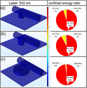
Figure 5. Simulation results of the hot spots distribution of three nanoparticle-nanowire-film systems with 532 nm laser irradiation. Both the radius of sphere in (a) and radius of cylinder in (b) are 200 nm. The major radius and minor radius of the torus in (c) are equal to 300 nm and 200 nm, respectively. The color bar is normalized to the incident source with unit electric field. The corresponding sector diagrams of confined energy ratio of each particle–wire nanostructure are shown at the right.
Download figure:
Standard image High-resolution image
Figure A1. (a)–(c) Simulation results of the hot spot distribution of three nanoparticle–nanowire–film systems under 633 nm excitation. The shape and size of nanostructures are the same with figure 5.
Download figure:
Standard image High-resolution image
In summary, energy is much more easily gathered at sharper contact areas, resulting in the hot spots being localized at the gaps. In particular, the hot spots are mainly distributed at the gap between the nanoparticle and nanowire under the 532 nm laser excitation in the system. These stable special properties are crucial to the wavelength modulated hot spot distribution and may lead to multiple applications.
5. Conclusions
Smooth, monocrystalline silver nanoparticles and nanowires were synthesized with the polyol method and showed excellent properties in our experiment. The SERS spectra of probing molecules both at the gap of silver nanoparticles and at the surface of thin gold film were investigated with the help of silver particle–wire nanostructures. Furthermore, the result also shows that the distribution of hot spots at the particle–wire joints exhibits an obvious wavelength dependence. The distribution of hot spots is highly sensitive to the excitation wavelength and the location of the hot spots can be varied by incident laser wavelength. Moreover, the geometric shape of the nanoparticles contributes little to the distribution, which makes the whole system more stable and easier to use for nanofabrication or chemical synthesis. The method we have demonstrated in this paper is not limited by the shape of nanoparticles; it makes significant progress in SERS detection and paves the way for further investigation.
Acknowledgments
This work was supported by the National Natural Science Foundation of China (Grant Nos. 11574038, 11004257 and 61575033), Chongqing Municipal Education Commission through grant No. KJ1400438 and Fundamental Research Funds for the Central Universities (CQDXWL-2012-016, 106112014CDJZR165503 and 106112016CDJXY300001), Natural Science Foundation Project of CQ CSTC (2014jcyjA40002 and 2011jjA90017) and Special Fund for Agro-scientific Research in the Public Interest (201303045).
: Appendix
Table A1. The electric field enhancement factor in each simulation picture.
| Figures under 532 nm | NP-NW | NP-film | NW-film |
|---|---|---|---|
| 2(d) | 95 | 0 | 8 |
| 3(d) | 77 | 7 | 6 |
| 5(a) | 175 | 38 | 7 |
| 5(b) | 67 | 18 | 8 |
| 5(c) | 102 | 11 | 8 |
| Figures under 633 nm | NP-NW | NP-film | NW-film |
|---|---|---|---|
| 2(d) | 76 | 17 | 30 |
| 3(d) | 78 | 78 | 30 |
| A1(a) | 160 | 230 | 42 |
| A1(b) | 285 | 23 | 45 |
| A1(c) | 176 | 56 | 51 |