
Abstract
Low voltage organic field-effect transistors (OFETs) using solution-processed cyanoethyl cellulose (CEC) and CEC-based nanocomposites as the gate dielectric are demonstrated. Barium strontium titanate (BST) nanoparticles are homogeneously dispersed in CEC to form the high-k (18.0 ± 0.2 at 1 kHz) nanocomposite insulator layer. The optimised p-channel DPPTTT OFETs with BST-CEC nanocomposite as the gate dielectric operate with minimal hysteresis, display field-effect mobilities in excess of 1 cm2 V−1 s−1 at 3 V, possess low subthreshold swings (132 ± 8 mV dec−1), and have on/off ratios greater than 103. Addition of a 40–50 nm layer of cross-linked poly(vinyl phenol) (PVP) on the surface of the nanocomposite layer significantly decreases the gate leakage current (<10−7 A cm−2 at ±3 V) and the threshold voltage (< −0.7 V) enabling operation of the OFETs at 1.5 V. The presented bilayer BST-CEC/PVP dielectrics are a promising alternative for the fabrication of low voltage, solution-processed OFETs that are suitable for use in low power, portable electronics.
Export citation and abstract BibTeX RIS

Original content from this work may be used under the terms of the Creative Commons Attribution 3.0 licence. Any further distribution of this work must maintain attribution to the author(s) and the title of the work, journal citation and DOI.
1. Introduction
Organic field-effect transistors (OFETs) are key components of low-cost, flexible and large area electronics. Extensive research has focussed on the development of solution-processed, high mobility organic semiconductors (OSCs) for these devices [1, 2], but recently attention is being directed towards the development of high-k gate insulators to enable low voltage operation [3, 4]. However, introducing solution-processed, high permittivity dielectric materials into high-performance, low-voltage OFETs is very challenging as there are a limited number of suitable high-k insulator materials that can be processed from solution. The commercialisation of portable devices such as printed sensor systems requires high yields of printed circuits that contain many OFETs. Therefore, the development of robust, flexible, pin-hole free, high capacitance gate dielectrics that can be processed from solution is urgently needed.
Theoretically, the gate dielectric areal capacitance (Ci) is directly proportional to the insulator dielectric constant, k, and inversely proportional to its thickness, d: Ci = ε0k/d. Typical organic dielectrics have relatively low dielectric constants (k ~ 2–4) [5, 6] and hence extremely thin layers (d < 20 nm) are required to obtain high Ci and deliver low voltage transistor operation. Organic FETs operating at 3 V using few nanometres of cross-linked polymer and polymer blends [7, 8], self-assembled mono- [9] and multi-layers [10] (SAMs) and polyelectrolytes [11, 12] have been demonstrated. Also, 1 V OFETs have been developed using ultra-thin, high-k, anodised Al2O3 and TiO2 insulators [13, 14]. However, thin dielectric layers may be prone to pin-holes and hence high leakage currents. Alternatively, solution-processed OFETs operating at 3 V using thick (d > 150 nm), high dielectric constant (k ~ 60) relaxor ferroelectric polymers [15], low-k and high-k polymer blends [16], and high-k nanocomposites [17] as the gate dielectrics have been reported. However, fabrication of organic FETs operating at or below 3 V using both solution-processed organic semiconductors and high-k dielectrics remains challenging.
Ceramic-polymer nanocomposites as gate dielectric materials have attracted much interest due to their simple processing, low cost and excellent properties, such as low dielectric loss and leakage current [18]. Organic FETs operating below 5 V using polymer/metal oxide nanocomposite dielectrics have been demonstrated [3, 19]. Although OFETs fabricated with nanocomposite gate dielectric showed improved transistor characteristics compared to the polymer only devices, hysteresis was not completely suppressed due to the presence of polar moieties in the dielectric layer. This hysteresis has resulted in a shift in VT and prevented the use of such dielectric layers in applications where stable VT is required. In addition, the leakage current density and dielectric breakdown strength were both adversely affected as the nanoparticle loading was increased. Recently, we have demonstrated 1 V OFETs that displayed minimal hysteresis using a solution-processed, bilayer dielectric layer consisting of PVP-capped high-k nanocomposite of BST-incorporated poly(vinylidene fluoride-co-hexafluoropropylene) (P(VDF-HFP) [20].
Herein, we show that low voltage OFETs operating below 3 V can be successfully fabricated in high yield (>90%) with low leakage current density (<10−7 A cm−2) and negligible device hysteresis using solution-deposited cyanoethyl cellulose (CEC) and CEC-based nanocomposite dielectrics. Also, it is demonstrated that application of a thin PVP film onto the nanocomposite surface significantly reduces the threshold voltage of the fabricated transistors enabling operation of the devices at 1.5 V. CEC is one of the most widely studied cellulose ethers and is prepared by reaction of cellulose with acrylonitrile [21]. When compared with poly(vinylidene fluoride) and its copolymers, CEC has good heat and acid stability, low moisture uptake and is mechanically robust. CEC with a high degree of substitution possesses relatively high values of dielectric permittivity (k ~ 14) and low values of dielectric loss at room temperature [22]. In addition, it has a considerably higher dielectric constant than that of most common organic polymers (k < 10) [23]. Recently, a high-k dielectric bilayer (Ci = 310 nF cm−2) composed of solution-processed cellulose (16 nm) on Al2O3 (8 nm) has been reported to deliver low voltage (<3 V) pentacene- and C60-based OFETs [24]. More recently, high-k nanocomposites of cyanoethyl cellulose and barium titanate (BTO) have been reported with k increasing to 27 at 90 % BTO loading. The enhanced dielectric permittivity was ascribed to the higher dielectric permittivity of BTO nanoparticles relative to that of CEC and the tight stacking of BTO nanoparticles in the nanocomposite (see [21]). Nevertheless, the use of cyanoethyl cellulose and CEC-based nanocomposites as the gate dielectric in OFETs has not yet been explored.
2. Experimental part
Cyanoethyl cellulose with the chemical structure shown in figure 1(a) was dissolved in N,N-dimethylformamide (DMF) at 1, 5 and 10 wt% and stirred for 3 h at room temperature until a homogenous solution was obtained. It has been found that 1 wt% solutions were too dilute and 10 wt% solutions too viscous to be reliably processed into thin films. As a result, 5 wt% CEC solutions were chosen as the optimal medium for the preparation of the nanocomposites. Then, 1, 5 and 10 wt% of BST nanoparticles (particle diameter <100 nm) were added into the prepared 5 wt% CEC solutions. To promote uniform dispersion of nanoparticles, the nanoparticle suspensions were ultra-sonicated for 2 h at 80 W and subsequently stirred for minimum 12 h. 1 wt% BST-CEC nanocomposites did not appreciably differ from the pristine CEC. In contrast, 10 wt% suspensions were very difficult to process. The nanoparticles quickly precipitated from solution resulting in highly inhomogeneous and unstable suspensions. Therefore, 5 wt% loading of BST nanoparticles was chosen as the optimal concentration for the formulation of BST-CEC nanocomposites. The 5 wt% nanocomposite suspensions were then centrifuged at 6000 rpm for 10 min to separate any larger particles and agglomerates to obtain uniform suspensions. The resultant BST-CEC solutions were stable for several weeks at room temperature. In order to operate transistors at 3 V while keeping the leakage current density to a minimum, the thickness and the areal capacitance of the BST-CEC dielectric layers were subsequently optimised by spin-coating the material at 1000, 2000, 3000 and 4000 rpm. The most desired film properties were obtained at 3000 rpm (see table 1). The thickness of the resulting dielectric films was measured using a DEKTAK 3ST profilometer. To evaluate the transistor performance, bottom contact OFETs were fabricated. As the active layer, either solution-processed poly(3,6-di(2-thien-5-yl)-2,5-di(2-octyldodecyl)-pyrrolo[3,4-c]pyrrole-1,4-dione)thieno[3,2-b] thiophene) (DPPTTT) [25] or a blend of 6,13-bis (triisopropylsilylethynyl) pentacene (TIPS-pentacene) and poly(α-methylstyrene) (PαMS) [26] were used. OFETs were fabricated on 1 cm2 Corning® glass substrates. Firstly, 80 nm thick aluminium layer was thermally evaporated to serve as the gate electrode. Then, pristine CEC or BST-CEC nanocomposite were spin-coated at 3000 rpm for 2 min and annealed under nitrogen at 90 °C for 90 min to form the dielectric layer. An optional capping layer of poly(4-vinyl phenol) (PVP) (20 mg ml−1) in propylene glycol monomethyl ether acetate (PGMEA) containing poly(melamine-co-formaldehyde) (PMF) (10 mg ml−1) as the cross-linking agent was spin-coated on top of the main dielectric layer at 5000 rpm for 2 min. The PVP layer was cross-linked at 130 °C for 90 min. Subsequently, gold source and drain electrodes (~50 nm) were thermally evaporated through a shadow mask. Au contacts were then modified by submersing samples in a 10 mM 2,3,4,5,6-pentafluorothiophenol (PFBT) solution in 2-propanol (IPA) followed by repeated washing with IPA. Finally, the semiconducting material was spin-coated from a solution in 1,2-dichlorobenzene (DCB) (5 mg ml−1) at 2000 rpm for 2 min and subsequently annealed under N2. Importantly, neither PGMEA nor DCB dissolved the thin films of cyanoethyl cellulose. Each glass substrate contained 18 capacitors or 9 transistors. The fabricated transistors had variable channel lengths L = 20–100 μm and a channel width W = 2000 μm. In each experiment four identical glass samples were simultaneously processed using both uncapped and PVP-capped CEC dielectrics. This resulted in 72 capacitors or 36 transistors fabricated simultaneously. For each batch of four samples, two DPPTTT and two TIPS-pentacene/PαMS OFETs were fabricated. At least 6 transistors on each glass substrate were successfully characterised and yields >90% were routinely achieved. The areal capacitance was measured using an Agilent E4980A Precision LCR Meter in the 100 Hz–2 MHz frequency range. The transistor characterisation was performed in ambient conditions (air with 40%–50% relative humidity) using an Agilent E5270B measurement mainframe with Karl Suss PH100 micromanipulator probes. AFM images were recorded on a Bruker Multimode 8 in Peak Force tapping mode at a resolution of 512 × 512 pixels.
Table 1. Parameters of the fabricated 3 V OFETs with cyanoethyl cellulose (CEC) and cyanoethyl cellulose nanocomposite (BST-CEC) films as the gate dielectric.
| OFET dielectric (semiconductor) | μ (cm2 V−1 s−1) | VT (V) | S (mV dec−1) | ON/OFF ratio |
|---|---|---|---|---|
| CEC (DPPTTT) | 0.6 ± 0.1 | −1.3 ± 0.2 | 145 ± 23 | ~104 |
| CEC (TIPS-pentacene/PαMS) | 0.1 ± 0.06 | −0.9 ± 0.3 | 470 ± 55 | ~103 |
| BST-CEC (DPPTTT) | 1.1 ± 0.1 | −1.4 ± 0.2 | 132 ± 8 | ~104 |
| BST-CEC (TIPS-pentacene/PαMS) | 0.4 ± 0.07 | −1 ± 0.4 | 177 ± 12 | ~103 |

Figure 1. (a) Structure of the fabricated bottom contact OFETs. Chemical structures of cyanoethyl cellulose (CEC) and DPPTTT, TIPS-pentacene/PαMS active layers are also shown. (b) Areal capacitance and (c) loss tangent of pristine and nanocomposite CEC films measured in 100 Hz–2 MHz frequency range.
Download figure:
Standard image High-resolution image3. Results and discussion
The structure of the fabricated bottom contact OFETs and the chemical structure of CEC dielectric and DPPTTT/TIPS-pentacene active layers are shown in figure 1(a). The dielectric properties of the pristine CEC and its nanocomposite films with and without PVP capping layer were evaluated by the fabrication of parallel-plate capacitors. The areal capacitance (Ci, nF cm−2) and loss tangent of the studied dielectric systems were measured in the 100 Hz–2 MHz frequency range. It can be seen that both the capacitance and the dielectric loss (loss tangent) of the pristine CEC and the nanocomposite with and without PVP have a relatively stable frequency response from 500 Hz to 100 kHz. As shown in figure 1(b), a consistent increase in Ci is measured for BST-CEC nanocomposite dielectric layers across the studied frequency range. At 1 kHz, Ci increased from 40.8 nF cm−2 for pristine CEC to 48.6 nF cm−2 for the BST-CEC nanocomposite films. An 8% reduction in Ci from 48.6 nF cm−2 to 44.5 nF cm−2 was measured after deposition of the PVP capping layer. As presented in figure 1(c), no significant variation in dielectric loss tangent (~0.02) was observed for the pristine polymer and its nanocomposite between 500 Hz and 100 kHz. At frequencies below 500 Hz, somewhat higher areal capacitance and slightly lower loss tangent were measured. On the contrary, at frequencies larger than 100 kHz the BST-CEC nanocomposite exhibited a visible decrease of its areal capacitance and the loss tangent increased sharply to 0.4. This is expected for most dielectrics and can be due to the dipole polarization of the CEC polymer and BST nanoparticles. At low frequencies the dipoles follow the change of field so that the dipole polarization makes a noticeable contribution to the increase of the dielectric permittivity of the nanocomposite films. In contrast, at high frequencies (f > 100 kHz) the dipoles do not have enough time to be polarized, thus the dielectric permittivity decreases as the frequency increases.
A typical output and transfer characteristics of p-channel DPPTTT OFETs using pristine CEC and BST-CEC nanocomposite dielectrics are shown in figures 2(a)–(d), respectively. The calculated parameters of the characterised transistors are presented in table 1. The saturated field-effect mobility μ and threshold voltage VT were found applying standard OFET theory [27]. The subthreshold swing S and on/off ratio were estimated from the transfer characteristics of the devices. The OFETs successfully operate below 3 V with small hysteresis showing saturated mobility values of 0.6 cm2 V−1 s−1 for pristine CEC and 1.1 cm2 V−1 s−1 for BST-CEC nanocomposites, respectively. For comparison, p-channel TIPS-pentacene/PαMS OFETs using pristine CEC and BST-CEC nanocomposite dielectric were also fabricated (see table 1). A representative output and transfer characteristics of p-channel BST-CEC TIPS-pentacene/PαMS OFETs are shown in figures 2(e) and (f). It can be noted that despite significantly smaller subthreshold swings and considerably increased field-effect mobility the BST-CEC nanocomposite OFETs display somewhat increased leakage current (~10−8 A at VGS = −3 V) when compared with CEC only devices (~10−9 A at VGS = −3 V). This could be due to the increased surface roughness of the nanocomposite films. One of the key challenges in the formation of high quality, high-k nanocomposite layers is to control the homogeneity of the nanoparticle dispersion and the stability of the nanocomposite suspension. Agglomeration of nanoparticles and phase separation from the polymer matrix, particularly at high filler loading, leads to an inhomogeneous mixture with poor processability, increased porosity and defect density [28]. Increased leakage current density, reduced dielectric breakdown strength and decreased dielectric constant are observed due to percolative pathways being created through the aggregated fillers [29]. Surface modification of the nanoparticles with a suitable coupling agent is one of the most widely used methods to prevent nanoparticle agglomeration [30]. As shown in our previous work (see [20]), by choosing the best combination of polymer matrix, organic solvents and nanoparticle-to-polymer volume ratio, stable, homogenous nanocomposite suspensions are prepared without the need for nanoparticle surface modification.
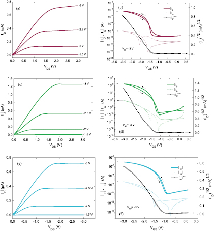
Figure 2. A typical output and transfer characteristics of bottom contact DPPTTT OFETs: (a) and (b) using pristine CEC, and (c) and (d) using BST-CEC nanocomposite dielectric. VSD = −3 V, channel width (W) = 2000 μm and channel length (L) = 80 μm and 60 μm, respectively. For comparison, a representative (e) output and (f) transfer characteristics of bottom contact TIPS-pentacene/PαMS OFETs using BST-CEC nanocomposite dielectric as the gate insulator is also shown. VSD = −3 V, channel width (W) = 2000 μm and channel length (L) = 70 μm.
Download figure:
Standard image High-resolution imageTo reduce the surface roughness and decrease the leakage current density, a thin layer of cross-linkable PVP was applied to the surface of the nanocomposite films. 1, 2, 5 and 10 wt% PVP solutions were spin-coated onto the BST-CEC dielectric layers at 5000 rpm for 2 min. BST-CEC capped with 1 wt% PVP showed no significant difference when compared with the uncapped nanocomposite films. On the contrary, the application of 5 and 10 wt% PVP resulted in significant drop of capacitance that value was comparable to the pristine PVP films of equivalent thickness. Hence, 2 wt% PVP was identified as the optimum concentration for the PVP capping layer. The thickness of the PVP capping layer was kept below 50 nm to cover the topographic features of the relatively rough nanocomposite surface without resulting in significant loss of capacitance. Figures 3(a) and (b) show tapping, contrast mode AFM images of uncapped and PVP-capped BST-CEC nanocomposite layers, respectively. The mV unit represents amplitude of the cantilever oscillation that is a measure of the relative stiffness of the sample's surface. As shown in table 2, a reduction of Ci from 48.6 nF cm−2 to 44.5 nF cm−2 was measured for PVP-capped BST-CEC films (see figure 1(b)). The deposition of the PVP layer lowered the RMS surface roughness of the nanocomposite film from 28 ± 5 nm to 13 ± 2 nm. Most importantly, as shown in figure 3(c), PVP-capping of the BST-CEC nanocomposite dielectric layer decreased the leakage current density well below 10−7 A cm−2 at ± 3 V. Subsequently, OFETs using PVP/BST-CEC nanocomposite layers as the gate dielectric were fabricated. As presented in figure 4, due to significantly reduced threshold voltage both DPPTTT and TIPS-pentacene/PαMS OFETs could successfully be operated at 1.5 V. The output and transfer characteristics of all fabricated transistors showed negligible hysteresis and the leakage current was reduced by at least one order of magnitude when compared to devices fabricated without the PVP capping layer. The average saturation field-effect mobility for the DPPTTT and TIPS-pentacene/PαMS OFETs with PVP-capped nanocomposite dielectric was calculated as 0.6 ± 0.1 cm2 V−1 s−1 and 0.30 ± 0.05 cm2 V−1 s−1, respectively. The mobility values for DPPTTT devices at such low operational voltage are noticeably higher than those reported previously [13]. However, the mobility values for TIPS-pentacene/PαMS OFETs are substantially lower [31]. The full set of transistor parameters for all fabricated devices with the PVP-capped BST-CEC as the gate dielectric is shown in table 3. The relatively small on/off ratio of the presented transistors is due to the three orders of magnitude larger off currents and much smaller on currents when compared with high on/off ratio pentacene transistors (on/off ⩾ 107) [32]. Whereas the much larger off currents were most likely caused by the leakage current through the gate insulator, the smaller field-effect mobility and low operational voltage of the devices were the possible reasons for significantly reduced on currents. The significant reduction of VT in OFETs with PVP-capped nanocomposite dielectric layer can be attributed to the reduced number of traps at the dielectric-semiconductor interface and/or dipoles in the dielectric layer. As reported by Mukherjee et al, the cross-linked PVP layer contributes to the reduction of carrier trapping sites at the interface between the gate insulator and the channel layer [33]. Despite operating at much lower voltage, DPPTTT OFETs using PVP-capped dielectric layers exhibited somewhat larger subthreshold swings. This could be due to the reduction of Ci in comparison to their uncapped counterparts. Interestingly, TIPS-pentacene/PαMS OFETs using PVP-capped nanocomposite dielectric showed smaller subthreshold swings S < 180 mV dec−1 and lower leakage current density at 1.5 V than those fabricated with DPPTTT. It appears that the vertical phase separation that contributes to a more robust interface with smaller number of traps may also occur in the dielectric systems studied here [34]. As a result, the presented approach is a promising alternative for the fabrication of low voltage, solution-processed OFETs that are suitable for use in low power applications such as portable electronics.
Table 2. Characteristics of pristine CEC and BST-CEC nanocomposite films with and without PVP capping layer.
| Dielectric | Ci (nF cm−2) | RMS (nm) | d (nm) | k |
|---|---|---|---|---|
| CEC | 40.8 ± 0.4 | 8 ± 2 | 285 ± 0.2 | 13 ± 0.1 |
| BST-CEC | 48.6 ± 0.3 | 28 ± 5 | 330 ± 0.7 | 18 ± 0.2 |
| BST-CEC with PVP | 44.5 ± 0.3 | 13 ± 2 | 378 ± 0.4 | 19 ± 0.2 |
Note: CEC and BST-CEC nanocomposite were spin-coated at 3000 rpm. Ci values were measured at 1 kHz.
Table 3. The calculated parameters of the fabricated 1.5 V OFETs with BST-CEC nanocomposite/PVP as the gate dielectric.
| OFET dielectric (semiconductor) | μ (cm2 V−1 s−1) | VT (V) | S (mV dec−1) | ON/OFF ratio |
|---|---|---|---|---|
| BST-CEC with PVP (DPPTTT) | 0.6 ± 0.1 | −0.7 ± 0.1 | 238 ± 17 | ~103 |
| BST-CEC with PVP (TIPS-pentacene/PαMS) | 0.3 ± 0.05 | −0.5 ± 0.1 | 170 ± 11 | ~103 |
Note: The values of the field-effect mobility (μ) were calculated in the saturation regime using Ci values measured at 1 kHz.
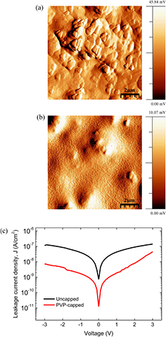
Figure 3. Tapping mode AFM images of (a) uncapped and (b) PVP-capped BST-CEC nanocomposite films. Images are shown in contrast mode. (c) Leakage current densities of the corresponding BST-CEC nanocomposite dielectric films with and without PVP capping.
Download figure:
Standard image High-resolution image
Figure 4. A typical output and transfer characteristics of (a) and (b) DPPTTT and (c) and (d) TIPS-pentacene/PαMS OFETs using PVP-capped BST-CEC nanocomposite dielectric as the gate insulator, respectively. VSD = −1.5 V, channel width (W) = 2000 μm and channel length (L) = 60 μm.
Download figure:
Standard image High-resolution image
4. Conclusions
In summary, low-voltage operating OFETs using solution-deposited, high-k gate dielectrics based on cyanoethylated cellulose (CEC) with polymeric and small molecule/polymer blend organic semiconductors are reported. The optimised p-channel DPPTTT OFETs were prepared in high yield (>90%), operated with minimal hysteresis, possess field-effect mobilities greater than 1 cm2 V−1 s−1 at 3 V, display small subthreshold swings smaller than 140 mV dec−1, and have on/off ratios larger than 103. The deposition of the thin PVP capping films onto the CEC-based dielectric layers significantly reduces the threshold voltage of the fabricated OFETs enabling realisation of ultralow voltage (<1.5 V) OFETs with much improved gate leakage current density characteristics. The presented CEC-based, high-k nanocomposite materials are promising alternative dielectrics for the fabrication of low-voltage, solution-processed OFETs that are suitable for use in ultralow power electronics.
Acknowledgments
This work was funded by UMIP and the EPSRC Centre for Innovative Manufacturing in Large Area Electronics (EP/K03099X/1).