

Abstract
Films composed of super-aligned single-walled carbon nanotubes (SWCNTs) have been widely used in electronic devices. Using first-principles calculations, we investigate the energetically most favorable stacking patterns and the electronic structures of SWCNT monolayers and bilayers formed by super-aligned (5, 5) and (7, 0) SWCNTs. It is found that the (5, 5) SWCNT monolayer prefers a 'face-by-face' stacking pattern with the binding energy of 13.90 meV/atom, whereas the (7, 0) SWCNT monolayer favors an 'edge-by-edge' pattern with the binding energy of 10.82 meV/atom. The (5, 5) SWCNT arrays are semiconducting with a band gap up to 114 meV for the bilayer, while the (7, 0) SWCNT arrays are metallic with a tiny overlap between valence and conduction bands, in sharp contrast to the cases of isolated (5, 5) and (7, 0) SWCNTs. This implies that weak van der Waals interactions between SWCNTs play an important role in applications of SWCNT films in electronic devices.
Export citation and abstract BibTeX RIS
Introduction
Single-walled carbon nanotubes (SWCNTs) are very attractive for electronic devices applications due to their superior geometry, good mechanical and extraordinary thermal conductivity [1]. These properties make them potential building blocks of carbon-based nanoelectronic devices [2–4]. An isolated SWCNT can be either metallic or semiconducting depending on its chirality and diameter. For electronic device applications, the orientation, density, diameter, electronic property and even the chirality of SWCNTs should be well controlled. In recent decades, tremendous efforts have been devoted to obtain monochiral carbon nanotubes [5–8]. Very recently, using high-melting-point alloy nanocrystals as catalysts, Li et al achieved the highly-selective growth of (12, 6) SWCNT [9]. This is a breakthrough for chirality control in SWCNT growth and will thus spur the development of SWCNT applications.
SWCNTs prefer to segregate into bundles via the van der Waals (vdW) interaction [9, 10]. Although the intertube vdW interaction is very weak compared to the C–C covalent bonds, the mechanical, optical and electronic properties of the bundles can be tuned by the alignment of SWCNTs as well as the chirality of the tubes [12, 13]. A theoretical work showed that when the chirality of the SWCNTs shares symmetry with the trigonal bundles structures, i.e. has a C6 axis, a pseudogap may be opened at the Fermi level depending on the orientation of the tube in the bundle [12]. Cho et al [11] pointed out that the optical property is also sensitive to the orientation of the tubes. They found the peak of the imaginary part of the dielectric function would be broadened in the bundle due to the intertube interaction, and an extra peak appeared at low energy due to the avoided crossing of the π and π* bands for (n, n) tube while n ≠ 3q (q = integer).
From the application point of view, a crucial step is to assemble individual building blocks into the desired architectures with predefined location and orientation. In this sense, super-aligned SWCNTs arrays represent one of the best candidates for SWCNT-based electronic devices [12, 13]. Super-aligned SWCNTs have been obtained on an ST-cut quartz substrate [14] and SiO2/Si substrates [15]. Although orientation-dependent properties of SWCNT bundles have been studied theoretically [11, 16–19] and experimentally [20], less work has been done for the 2D SWCNT array. For SWCNTs with a C6 axis, the bundles having a C6 axis would have an identical intertube contact pattern at a certain degree rotation [21]. However, for SWCNTs without a C6 axis, the contact patterns are quite complicated in the bundles and the role of each pattern is difficult to figure out. The complex contact patterns would further offer large degrees of freedom for the fine tuning of electronic structures of SWCNT.
In this contribution, we investigate the SWCNT nanofilms of super-aligned SWCNTs. Without loss of generality, we chose a (5, 5) and a (7, 0) SWCNTs as building blocks, both of which are free from a C6 axis tube. (5, 5) SWCNT is metallic, whereas (7, 0) SWCNT is a semiconductor. Using first-principles calculations, we show that these two types of SWCNTs prefer different intertube contact patterns, therefore resulting in different electronic structure modification when assembled to a monolayer or a bilayer. From the energetic point of view, the metallic (5, 5) tubes prefer a 'face-to-face' pattern, whereas the semiconducting (7, 0) tubes favor an 'edge-to-edge' pattern. More interestingly, the nanofilms formed by aligning metallic (5, 5) SWCNTs become semiconductive with a band gap up to 114 meV, while those composed of semiconducting (7, 0) SWCNTs are metallic with a tiny overlap between valence and conduction bands.
Computational methods
Our calculations were performed under the framework of density functional theory (DFT) as implemented in the VASP package [22–24]. Exchange and correlation effects were treated self-consistently with a generalized gradient approximation (GGA) using a Perdew–Burke–Ernzerhof (PBE) exchange-correlation functional [25]. Electron-ion interactions were described by the projector augmented plane-wave method (PAW) [26, 27]. Electron wavefunctions were expanded in a plane-wave basis set with an energy cutoff of 500 eV. The vdW correction (DFT-D2) within the PBE functional proposed by Grimme [28] was employed in dealing with the interaction between carbon nanotubes [29]. The geometries of the isolated SWCNTs were first optimized using a conjugate gradient (CG) scheme without any symmetric restriction until the total energy and Hellmann–Feynman forces are convergent within 10−5 eV and 0.01 eV Å−1 respectively, and then assembled into the SWCNT monolayer or bilayer. For the isolated SWCNTs with small sizes, the Brillouin zone was sampled on grids of 5 × 5 × 45 within the Gamma center scheme, while for the SWCNT monolayer and bilayer with large supercells, they were set to 3 × 3 × 25 and 15 × 15 × 5 to save computational resources. Using the above-mentioned strategy, the tube radii of (5, 5) and (7, 0) were calculated to be 6.83 Å and 5.60 Å, which are in agreement with previous works [11, 30]. The binding energy between SWCNTs in the nanofilms is defined by the difference between the total energy of the nanofilm and the sum of total energies of isolated SWCNTs.
Results and discussion
1. SWCNT monolayer
We first consider a super-aligned SWCNT monolayer. There are numerous patterns for SWCNTs depending on the rotation angle and the displacement between them when they are assembled into a super-aligned monolayer. The works of graphene multi-layers have shown that the energetically most favorable patterns always have high symmetries, e.g. the Bernal-stacking pattern (AB). Therefore, in this work, we focus on four high-symmetric contact patterns corresponding to four specific rotation angles of the SWCNTs, as depicted in figure 1. We distinguish different stacking ways by contact surfaces. For the AA-1, the adjacent SWCNTs form an 'edge-to-edge' contact pattern, whereas the AA-2 is very similar to the AA stacking pattern in graphene multilayers, except for the curved surfaces of SWCNTs. Both the AB-1 and AB-2 patterns are analogous to the Bernal-stacking (AB) in graphene with different displacements. The AB-2 pattern for (7, 0) SWCNT is very similar to the AB pattern for graphene. The symmetry depends on the arrangement of the neighboring tubes. The AA patterns have a mirror plane between two neighbor tubes, while AB patterns have glide reflection planes.
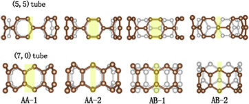
Figure 1. Side view of four contact patterns of monolayer super-aligned nanotube arrays. The pale yellow facets denote the contact surface on the nanotube. The grey white and dark brown balls represent the back and front carbon atom, respectively.
Download figure:
Standard image High-resolution imageThe equilibrium distance between two adjacent tubes in this SWCNT monolayer was then determined by performing first-principles calculations using different exchange-correlation functionals. The total energy as a function of intertube distance is plotted in figure 2. It is evident that both the (5, 5) and (7, 0) SWCNT monolayers exhibit very similar characteristics. By means of PBE functional with vdW correction (PBE+vdW), our calculations show that the AB-1 pattern is energetically most favorable for these two types of SWCNT monolayers. The binding energies are 13.90 meV/atom and 10.82 meV/atom for (5, 5) and (7, 0) SWCNT monolayers, respectively. The interlayer distances between contact surfaces of two adjacent tubes are 2.9 Å for (5, 5) SWCNTs and 3.0 Å for (7, 0) SWCNTs, which are slightly shorter by about 0.1 Å than those obtained from the LDA functional. This is very similar to the case of bilayer graphene whose energetically most favorable pattern is a Bernal stacking pattern with an interlayer distance of 3.1 Å [32, 33]. However, without the vdW correction, the PBE functional fails to give a stable binding state, because the total energy decreases monotonously with the increase of intertube distance. Therefore, involving vdW correction in the calculation is very important and convincing in this work. A similar feature has also been found in BN/graphene heterostructures [31, 32].
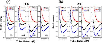
Figure 2. Relative energies per unit of SWCNTs monolayers as a function of intertube distance using LDA (black square point), PBE (red circle point), and vdW (blue up-triangle point) functionals for (a) (5, 5) and (b) (7, 0) SWCNT monolayers in four different contact patterns (see figure 1). Relative energies are measured by the difference between the total energy of the nanofilm and the sum of the total energies of corresponding isolated SWCNTs.
Download figure:
Standard image High-resolution imageWe also evaluated the equilibrium intertube distances and the binding energies of other metastable patterns and listed them in table 1. Detailed analysis indicates that the intertube distances vary between 3.2 and 3.4 Å for the AA patterns, which are very close to the interlayer distance in graphite, 3.3 Å [33], and the intertube distances of 3.2 ~ 3.4 Å in carbon nanotube bundles [9, 17, 30, 34, 35]. The AA patterns have longer intertube distances than the AB patterns by about 0.2 ~ 0.5 Å, due to the subtle balance between vdW and Pauli interactions. The binding energy per atom of the SWCNT monolayers are lower than that in graphite and carbon nanotube bundles [30], which can be ascribed to less contact area in the SWCNT monolayers.
Table 1. Intertube distances and the vdW interaction energies (per atom and per length) of SWCNT monolayers with different chiralities and contact patterns.
| D (Å) | Evdw (meV/atom) | Evdw (meV Å−1) | |
|---|---|---|---|
| (AA-1)(5, 5) | 3.3 | 7.25 | 58.75 |
| (AA-2)(5, 5) | 3.4 | 7.60 | 61.59 |
| (AB-1)(5, 5) | 2.9 | 13.90 | 112.64 |
| (AB-2)(5, 5) | 3.0 | 8.95 | 72.53 |
| (AA-1)(7, 0) | 3.3 | 8.32 | 54.53 |
| (AA-2)(7, 0) | 3.2 | 8.18 | 53.59 |
| (AB-1)(7, 0) | 3.0 | 10.82 | 70.91 |
| (AB-2)(7, 0) | 3.0 | 10.36 | 67.87 |
Next we examined the electronic structures of the SWCNT monolayers with different patterns. The electronic band structures and the total density of states (TDOS) of the SWCNT monolayers at equilibrium are plotted in figure 3. Isolated (5, 5) SWCNT is metallic, while isolated (7, 0) SWCNT is a narrow band gap semiconductor. For the SWCNT monolayer, however, the electronic structures are modified due to the intertube interaction and exhibit the stacking-pattern dependence. The Dirac cone of (5, 5) SWCNT is preserved in the AB-1 pattern, the energetically most favorable pattern, but vanishes for other patterns. A small pseudogap of about 28 ~ 98 meV is opened for the AA and AB-2 patterns. It is noteworthy that there is a slight shift of the two sub bands for the AA-2 and AB-2 patterns because of the absence of translational symmetry. The electronic structure modification can also be reflected by the TDOS shown in figure 3(b). The overall shapes of TDOS are similar, except for the appearance of the electronic states near the Fermi level. AB-1 contacting pattern has a high DOS at the Fermi level and thus is metallic.
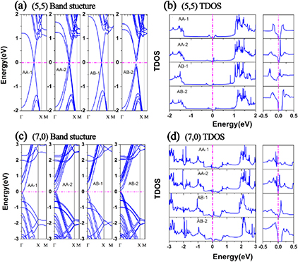
Figure 3. Electronic band structures and total density of states (TDOS) of the super-aligned SWCNT monolayer with contact patterns (see figure 1). (a) Band structure along high-symmetric points and (b) TDOS for (5, 5) SWCNT monolayers, with an expanded energy scale of total density of states at the right panel. (c) and (d) are the band structures and TDOS for (7, 0) SWCNT monolayers, respectively. Energy is measured from the Fermi level.
Download figure:
Standard image High-resolution imageThe electronic structures of the (7, 0) SWCNT monolayer exhibit different features. The AA patterns (AA-1 and AA-2) are metallic. The valence bands and conduction bands shift upward and downward respectively, leading to a tiny overlap between valence and conduction bands, as shown in figure 3(c). For the AB patterns, the band gap is preserved. These results clearly imply that the electronic structures of SWCNT monolayer can be tuned by changing the stacking pattern.
2. SWCNT bilayer
The atomic structures of SWCNT bilayers are built by stacking two SWCNT monolayers. In each monolayer, the SWCNTs are arranged in the energetically most favorable patterns as described in the previous parts. The two SWCNT monolayers are then assembled in three typical patterns: two parallel patterns (M and T) and one perpendicular pattern (P), as shown in figure 4. For the M pattern, the SWCNT of the top layer is located right in the middle of two SWCNTs of the down layer, as shown in figure 4(a), while it is right above the SWCNT of the down layer in the T pattern, as shown in figure 4(b). The P pattern has two layers of SWCNTs perpendicular to each other, as shown in figure 4(c). The optimized interlayer distances and the relevant binding energies between the two layers are listed in table 2. For both (5, 5) and (7, 0) SWCNTs, the P pattern has the shortest interlayer distance, whereas the T pattern has the longest one. It is interesting to see that the M pattern is energetically the most favorable for the (5, 5) SWCNT bilayer, while the P pattern is energetically the most favorable for the (7, 0) SWCNT bilayer.
Table 2. Intertube distances and vdW interaction energies (in eV/atom and eV Å−2) of the SWCNT bilayers with different chiralities and stacking patterns.
| D (Å) | Evdw (meV/atom) | Evdw (meV Å−2) | |
|---|---|---|---|
| M(5, 5) | 3.2 | 8.69 | 14.48 |
| T(5, 5) | 3.3 | 4.16 | 6.93 |
| P(5, 5) | 2.9 | 5.02 | 8.24 |
| M(7, 0) | 3.1 | 9.11 | 13.89 |
| T(7, 0) | 3.3 | 5.56 | 8.48 |
| P(7, 0) | 3.0 | 11.95 | 18.32 |
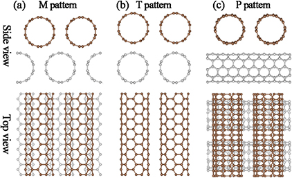
Figure 4. Side view and top view of three stacking patterns of super-aligned SWCNT bilayers. Different color (grey white and dark brown) balls are used to distinguish atoms belonging to different nanotube layers.
Download figure:
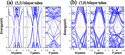
Standard image High-resolution imageThe electronic band structures of the SWCNT bilayers are calculated along the high-symmetric lines in the 2D Brillouin zone, as shown in figure 5. The (5, 5) SWCNT bilayer in the M pattern, the energetically most favorable pattern, is semiconducting with a band gap of 195 meV along the M-X direction and 114 meV along the M-Γ direction, as shown in figure 5(a). While the bilayers with the other two patterns are metallic. The two Dirac cones along the M-X and M-Γ directions are preserved in the P pattern. The (7, 0) SWCNT bilayers considered in this work, however, are all metallic, independent of the stacking pattern, as shown in figure 5(b). These features differ significantly from those of SWCNT monolayers and isolated SWCNTs, suggesting a possible route to tune the electronic properties of SWCNTs.
Figure 5. PBE + vdW band structures of the (a) (5, 5) and (b) (7, 0) SWCNT bilayer with three typical stacking patterns (see figure 4). Energy is measured from the Fermi level.
Download figure:
Standard image High-resolution image
Conclusions
Using first-principles approaches including vdW corrections, we give a comprehensive characterization of structural and electronic properties of super-aligned SWCNT monolayers and bilayers. Our attention is directed to the contact pattern dependent coupling between SWCNTs. The equilibrium distances vary from 2.9 to 3.4 Å for the SWCNT monolayer as a result of competition between Pauli and vdW interactions. Binding energy calculations indicate that AB-1 is the most stable pattern for (5, 5) and (7, 0) SWCNT monolayers. There exist profound differences of electronic structures between SWCNT nanofilms and isolated SWCNTs near the Fermi level. For the (5, 5) SWCNT monolayer, a small band gap is opened as the SWCNTs are assembled with the AA-1, AA-2 and AB-2 contact patterns, leading to a metal-semiconductor transition. The valence band and the conduction band of the (7, 0) SWCNT monolayer move upward and downward respectively, resulting in the disappearance of the band gap for AA-1 and AA-2 contact patterns. The (5, 5) SWCNT bilayer with the M pattern, the energetically most favorable pattern, shows a relatively large gap, ~114 meV. The (7, 0) SWCNT bilayers are metallic independent of stacking patterns. A detailed study of the stable stacking patterns and electronic changes of super-aligned SWCNT nanofilms will be of great importance for its application in nanoelectronic devices.
Acknowledgments
This work is supported by the National Basic Research Program of China (No. 2012CB932302), the National Natural Science Foundation of China (No. 91221101, No. 11375108), the 111 project (No. B13209) and National Super Computing Centre in Jinan.