Abstract
The Glenn Research Centre of NASA, USA (www.grc.nasa.gov/WWW/SiC/, silicon carbide electronics) is in pursuit of realizing bulk manufacturing of silicon carbide (SiC), specifically by mechanical means. Single point diamond turning (SPDT) technology which employs diamond (the hardest naturally-occurring material realized to date) as a cutting tool to cut a workpiece is a highly productive manufacturing process. However, machining SiC using SPDT is a complex process and, while several experimental and analytical studies presented to date aid in the understanding of several critical processes of machining SiC, the current knowledge on the ductile behaviour of SiC is still sparse. This is due to a number of simultaneously occurring physical phenomena that may take place on multiple length and time scales. For example, nucleation of dislocation can take place at small inclusions that are of a few atoms in size and once nucleated, the interaction of these nucleations can manifest stresses on the micrometre length scales. The understanding of how these stresses manifest during fracture in the brittle range, or dislocations/phase transformations in the ductile range, is crucial to understanding the brittle–ductile transition in SiC. Furthermore, there is a need to incorporate an appropriate simulation-based approach in the manufacturing research on SiC, owing primarily to the number of uncertainties in the current experimental research that includes wear of the cutting tool, poor controllability of the nano-regime machining scale (effective thickness of cut), and coolant effects (interfacial phenomena between the tool, workpiece/chip and coolant), etc. In this review, these two problems are combined together to posit an improved understanding on the current theoretical knowledge on the SPDT of SiC obtained from molecular dynamics simulation.
Export citation and abstract BibTeX RIS

Content from this work may be used under the terms of the Creative Commons Attribution 3.0 licence. Any further distribution of this work must maintain attribution to the author(s) and the title of the work, journal citation and DOI.
This article was made open access on 5 January 2014
Abbreviations
| ABOP | analytical bond order potential |
| BDT | brittle–ductile transition |
| BOP | bond order potential function |
| CBN | cubic boron nitride |
| CIS | critical indent size |
| CMP | chemo-mechanical polishing |
| DBT | ductile to brittle transition |
| DXA | dislocation extraction algorithm |
| EUV | extreme ultraviolet |
| HPPT | high pressure phase transformation |
| IR | infrared |
| LAM | laser assisted machining |
| MEMS | micro-electro-mechanical system |
| MD | molecular dynamics |
| MRF | magneto rheological finishing |
| MRR | material removal rate |
| NEMS | nano-electro-mechanical system |
| RAF | repeated a-face growth process |
| RDF/g(r) | radial distribution function |
| SiC | silicon carbide |
| SDM | surface defect machining |
| SPDT | single point diamond turning |
| TRISO | tristructural-isotropic fuel |
| UPM | ultra-precision manufacturing |
| VLSI | very-large-scale integration |
Nomenclature
| α | numerical parameter |
| a | lattice constant |
| a0 | depth of cut |
| c | critical crack length |
| dc or tc | critical chip thickness |
| E | elastic modulus of the material |
| G | bulk modulus of the material |
| H | hardness of the material |
| Kc/R | fracture toughness of the material |
| Kb | Boltzmann constant (1.3806503 × 10⁻²³ J/K) |
| lc | length of contact between cutting chip and tool |
| R | nose radius of the cutting tool |
| r | inter-atomic distance |
| S | specific energy required to propagate a crack |
| tmax | maximum critical undeformed chip thickness |
| V | cutting speed |
| W | width of cut |
| Wd/Zeff | ductile width of cut |
| Yc | critical crack length |
| ρ | density of the material |
| σy | yield stress for plastic flow |
1. Silicon carbide
1.1. Background and demand of SiC manufacturing
Ultra-hard brittle materials exhibit extreme hardness due to their covalent and ionic bonds. An interesting feature which all such materials share is the short sp3–sp3 bond length. In general, they can be represented using the 'composition cycle' shown in figure 1 [2]. This cycle consists of the four elements, i.e. carbon (C), boron (B), silicon (Si) and nitrogen (N) and the combination of any two produces a three-dimensional covalently bonded compound exhibiting ultra-high hardness, e.g. diamond, cubic boron nitride (CBN), SiC, Si3N4, B4C, SiB6 and the recently recognized C3N4. Both diamond (the hardest naturally-occurring material identified to date) and silicon carbide are classified as hard and brittle [3] due to their sp3-bonded nature and shorter bond length. Under ambient conditions, nitrogen is gaseous with only diatomic covalent bonds while boron, silicon and diamond (carbon) naturally form three-dimensionally covalent solids [2]. Although all these materials exhibit different advantages, SiC offers its own unique and exceptional properties such as chemical inertness, high thermal conductivity, high carrier saturation velocity, high specific stiffness (E/ρ) and high-temperature resistance [4]. For these advantages, SiC is emerging as a prime candidate for several engineering applications which were historically reserved for soft metals, and hence close tolerances and good surface finish are of prime concern. However, mechanical processing of SiC is a daunting task (even using state-of-the-art technologies) owing primarily to the following unique characteristics of SiC [5, 6]:
- 1.SiC exhibits a low thermal coefficient and high thermal conductivity. This is because of the higher proportion of covalent bonding compared to ionic bonding in SiC (9 : 1) with the nature of bonding dependent on the Goldschmidt number. The higher proportion of covalent bonding in SiC makes the brittle phase of SiC insensitive to high temperature deformation.
- 2.In general, the ratio of Young's modulus and Vickers hardness in brittle materials is only about 20. This is in contrast to soft ductile materials where this ratio could be as high as 250. For materials like SiC, nanoindentation hardness is a more appropriate measure and the ratio of Young's modulus and nanoindentation hardness of SiC is comparatively higher than that of metals, which signifies that SiC is highly brittle.
- 3.The ratio of tensile strength to shear strength in SiC is extremely low (∼1.5) in contrast to soft ductile metals where this ratio is as high as 10, making them easier to deform through plastic deformation rather than brittle fracture.
- 4.Low density and low mobility of dislocations leads to high hardness in SiC, while low surface energy due to a small density of electrons and a high Young's modulus are the reasons for the extreme brittleness in SiC. Owing to low surface energy and a high Young's modulus, SiC exhibits low fracture toughness and thus poor machinability.
- 5.To induce the plastic deformation in a ceramic material such as SiC, it requires five independent slip systems to meet the von Mises criterion, otherwise twinning or fracture prevails.

Figure 1. Composition cycle of hard, brittle materials [2].
Download figure:
Standard image High-resolution imageConsidering the high hardness of SiC, the hardest naturally occurring material, diamond, appears to be the only viable choice to cut SiC. A hardness ratio of 5 : 1 between the cutting tool and the workpiece is normally recommended for machining [7], however, this ratio in the case of the diamond tool: SiC (3C type), is about 4 : 1 owing to the high micro hardness of 3C–SiC (about 25–30 GPa) against diamond (100 GPa). It has been experimentally found that nano hardness of SiC, depending on the polytype, can vary in the range of 55–70 GPa for lower depth of cuts below 50 nm [7]. Therefore, below a cut depth of less than 50 nm, the hardness ratio of tool:workpiece reduces further to around 2 : 1 and consequently the diamond tool faces tremendous cutting resistance [7]. Due to the above complex challenges, many advances have evolved in the area known as ultra-precision engineering. The key drivers of accuracy in ultra-high-precision manufacturing having finely textured surfaces and features has attracted a lot of scholars [8]. While these demands previously arose from defence and weapon programmes, recent research is shifting emphasis towards renewable energy generation, promotion of green energy processes and environmental sustainability [9].
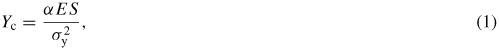
To index SiC to other brittle materials, a property map of various hard materials with respect to their hardness (H) and elastic modulus (E) is shown in figure 2. Traversing the range of hard and brittle materials shown in figure 2, it can be seen that nanocrystalline diamond exhibits the highest hardness and Young's modulus, followed by CBN, SiC, Si3N4 and silicon. Also, while elastic modulus (E) and hardness (H) are important indicators to assess the mechanical properties, their ratio carries a particular importance. For example, nano-scratching tests performed on a wide range of materials from polymers to metals have revealed that the extent of plastic deformation increases with increasing E/H ratio [11]. On the basis of such tests, it has been concluded that the E/H ratio provides a good criterion to assess the machinability of a material [12]. However, it has been asserted that when the E/H ratio along a certain crystal direction is high, this may not necessarily provide ample information regarding the plastic response [13]. This directional sensitivity may occur if there is a large difference in the hardness and transition pressure (pressure required to cause phase transformation) along a particular direction, which may result in the initiation of undesirable fragile cracks. Puttick et al [14] have noted that in such circumstances, yielding may occur in brittle materials rather than a crack propagation. The extent of the crack does not go past a certain critical dimension known as the critical crack length (Yc) which is expressed as follows:
where E is young's modulus, σy is the yield stress, S is the specific energy required to propagate a crack and α is a numerical parameter which depends on the type of process involved such as indentation, compression or scratching.
Figure 2. Variation in the hardness and Young's modulus of various materials. Reprinted with permission from [10], Copyright 2001 Nature.
Download figure:
Standard image High-resolution imageIt is interesting to note that Inasaki [5] cited Taniguchi [15, 16], who coined the term nanotechnology in the early 1980s to highlight the concept of the 'machining unit' or 'size scale' (figure 3). Figure 3 highlights the fact that a change in length scale leads to a change in the mode of material removal during contact loading (nanoimpact, nanoindentation, nanometric cutting, etc) especially for the brittle materials. Inasaki classified this size scale broadly into four domains. Each domain highlights the change in the mode of deformation consequent to the change in the size at which the material is processed. It is thus crucial to understand the importance of the length scale (the associated geometry due to shape factor) as well as the time scale at which brittle materials such as SiC can be processed more effectively.

Figure 3. Factors affecting deformation of material with respect to size scale.
Download figure:
Standard image High-resolution image1.2. Applications and commercial availability of SiC
Ceramics such as SiC and semiconductors such as silicon and germanium (C, Si, Ge and even tin are in the same group in the periodic table) share a common characteristic of being nominally hard and brittle. Silicon carbide (SiC) is an extremely hard and brittle non-oxide ceramic material. Due to its semiconducting properties, and due to it being highly oxidation and wear resistant (chemical + mechanical + thermal), use of SiC in the semiconductor electronics has been found advantageous in many areas compared to the current silicon based very-large-scale integration (VLSI) technology. Other potential areas of SiC include its use for quantum computing applications [17–19], space-based laser mirrors [20], mirrors for surveillance and vacuum ultraviolet telescopes, as fuel atomizers for the gas turbine engines (SiC was able to perform beyond 2.5 MPa while Si can barely work beyond 1.4 MPa) [21] and for the development of thermal protection system materials for defence applications [22]. The demand for SiC is growing further in weapons, aerospace, microelectronic, bio-imaging [23] and bio-medical applications [24] as well as in 'big-science' programmes such as the European Extremely Large Telescope (E-ELT), the Atacama Large Millimeter/submillimeter Array (ALMA) [25] and next generation extreme ultraviolet (EUV) lithography steppers. SiC has high corrosion resistance due to its strong chemical bond energy, i.e. the cohesive energy of 3C–SiC is 6.34 eV/atom which is the reason it is also a prime candidate for fourth generation nuclear power plants [26]. Particularly, the tristructural-isotropic (TRISO) fuel intended to be used for such reactors warrants a fuel kernel of uranium oxide (UOx) coated in several layers of materials with different functions and SiC can well be used for such a purpose [27].
SiC is also finding amazing applications in the bio-medical sector especially as a semi-conductor material because of being more bio-compatible than silicon. Traditional orthopaedic materials such as cobalt chrome (CoCr), stainless steel and titanium, on account of being low wear and oxidation resistant, succumb to bone loss which causes implant loosening resulting in a reactive implant surface. SiC is capable of permanently integrating into the new bone growth on account of low wear debris and metallosis and is thus very effective as a coating for stents to enhance hemocompatibility and as a coating for prosthetic-bearing surfaces and uncemented joint prosthetics [28]. Due to these developments, SiC can be considered as a potential candidate to outperform silicon based components in the context of a range of commercial opportunities, as summarized in table 1 [1].
Table 1. Commercial applications of SiC [29].
| S.No. | Properties of SiC | Applications | Realization |
|---|---|---|---|
| 1 | High sublimation temperature | High temperature transducer elements | High temperature sensor diaphragms and resonators |
| 2 | Large band gap | High temperature electronics | Sensors for smart engines |
| On chip signal conditioning | |||
| 3 | Low wear and high hardness | Enhanced durability/operation | Coated mechanical contacts |
| Microfabricated bearings | |||
| 4 | Chemically inert | Stable in harsh environments | Valves/pumps for corrosives |
Figure 4 shows some of the useful applications of SiC. These include using it as an electronic chip for large scale quantum computing technology [18], as an atomizer [21], as a primary telescopic mirror [20], as a nanopattern mould [30] and as a lateral resonator device for MEMS systems [31]. While SiC is being found useful for amazing applications across several engineering disciplines, it is still a challenge to procure SiC in any given shape and size. This is because of the ongoing technological developments in the SiC crystal growth technology which is still in its infancy. After years of research on the sublimation growth process, Cree Research became the first company to sell 2.5 cm diameter wafers in the year 1990 (figure 5). Since then, a number of companies have emerged who now sell SiC wafers that are significantly larger in diameter. Currently, single crystals of SiC are grown using a method called physical vapour transport. Madar [32] has reported that a new process named 'repeated a-face growth process (RAF)' has shown promise to develop virtually dislocation-free, large sized SiC wafers. Table 2 lists (not exhaustive) some of the major suppliers across the globe who now supply SiC wafers.

Figure 4. (a) Silicon carbide wafer showed tantalizing prospects to realize large scale quantum computing technology. Reprinted with permission from [18], Copyright 2011 Nature. (b) SEM photo of SiC atomizer. Reprinted with permission from [21], Copyright 1999 IEEE. (c) Herschel space telescope 3.5 m diameter SiC based primary mirror. Reprinted with permission from [20], Copyright 2010 CRC Press LLC. (d) SiC being used as a nanopattern mould. Reprinted with permission from [30], Copyright 2007 CRC Press LLC. (e) SiC based lateral resonator device for MEMS systems. Reprinted with permission from [31], Copyright 2000 CRC Press LLC.
Download figure:
Standard image High-resolution image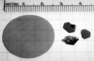
Figure 5. First ever mass produced 25 mm 6 H–SiC wafer made available by Cree research in the year 1990. Reprinted with permission from [31], Copyright 2000 CRC Press LLC.
Download figure:
Standard image High-resolution imageTable 2. Major manufacturers of SiC wafers/films.
| S.No. | Manufacturer | Contact/website | Country |
|---|---|---|---|
| 1 | Cree Research Inc. | www.cree.com | USA |
| 2 | MTI Corporation | http://mtixtl.com/ | USA |
| 3 | POCO Graphite | www.poco.com | USA |
| 4 | Aymant Technology Inc. | www.aymont.com | USA |
| 5 | Dow Corning | www.dowcorning.com | USA |
| 6 | Technologies and Devices International, Inc | http://www.tdii.com | USA |
| 7 | Glenn Research Centre, NASA | http://www.grc.nasa.gov | USA |
| 8 | CoorsTek | www.coorstek.com | USA |
| 9 | Boostec | jlavenac@boostec.com | USA |
| 10 | Japan Fine Ceramics Company Limited | s_ishii@japan-fc.co.jp | Japan |
| 11 | Hoya | http://www.hoya.co.jp | Japan |
| 12 | Nipponsteel | www.nsc.co.jp | Japan |
| 13 | Semiconductor Wafer Inc. | sales.europe@semiwafer.com | Japan |
| 14 | Xiamen Powerway Advanced Material Company Limited | sales@qualitymaterial.net | China |
| 15 | SiCrystal AG | Peter.Sasahara@sicrystal.de | Germany |
| 16 | NOVASiC | mmarsan@novasic.com | France |
| 17 | Norstel | http://www.norstel.com | Sweden |
Compared to silicon and germanium wafers which are relatively easier to process by mechanical and/or chemical means, SiC wafers are relatively smaller, more expensive and of inferior quality in terms of flatness and surface roughness. This disparity is not surprising considering that silicon and germanium have undergone several years of commercial research while research on SiC is still progressing. Nevertheless, on-going research endeavours would eventually alleviate wafer surface quality deficiencies. Crystals of SiC once grown are sliced, ground and polished to achieve atomic flatness using cost intensive technologies [33]. At such a finite precision of roughness, surface forces dominate in influencing the system response of MEMS and NEMS systems [34]. The adhesion or 'stiction' exhibited by such fine surfaces is a precursor to the life of the components as it resists the relative motion between the two parts. It has been recently explained that this adhesion arises from the van der Waals dispersion forces acting across the contact asperities [35]. Therefore, modification of the SiC surface with a finite level of precision requires an accurate understanding of the relevant atomistic mechanisms. Hence, nanometric cutting of SiC by a single point cutting tool presents many technical challenges, and a lot of current research is ongoing to explore its nanometric cutting [36–38].
1.3. Crystallography and polymorphism in SiC
SiC exhibits one-dimensional polymorphism i.e. all polytypes have the same tetrahedral arrangement of Si and C atoms but different stacking sequences (figure 6). This means that even though all SiC polytypes consist of 50% carbon atoms covalently bonded with 50% silicon atoms, each SiC polytype has distinct electrical and mechanical properties. The stacking sequence of the Si-C bilayers along [111] or [0 0 0 1] direction distinguishes all the polytypes of SiC, amongst which the most common polytypes are cubic (3C or β-SiC), hexagonal (2H, 4H and 6H) or α-SiC and rhombohedral (15R) type SiC [39]. The numbers here refer to the number of repeating layers in the unit cell while the letter designates the crystal structure, where C=cubic, H=hexagonal and R=rhombohedral.

Figure 6. Polymorphism in SiC. Reprinted with permission from [40], Copyright 2012 Elsevier. (a) Tetrahedral geometry of SiC and (b) stacking sequence of bilayers in polytypes of SiC.
Download figure:
Standard image High-resolution imageFrom figure 6, it may be seen that if the first Si-C layer is labelled A, a close packed structure can be obtained by placing the next layer at either of the positions B or C. Various polytypes of SiC are simple permutations of three such positions. Thus defined, the stacking sequence is ABC in 3C–SiC, ABCB in 4H–SiC and ABCACB in 6H–SiC. Note that β-SiC is formed at temperatures below 1973 K [7] while α-SiC is formed generally at temperatures greater than 1973 K. An orthographic view of the unit cell of 3C–SiC and 4H–SiC is shown in figure 7 while a more detailed view of 4H–SiC is shown in figure 8 where the green and red colours1 correspond to silicon and carbon atoms respectively.

Figure 7. Unit cell of SiC. (a) Orthographic view, 3C–SiC and (a) orthographic view, 4H–SiC.
Download figure:
Standard image High-resolution image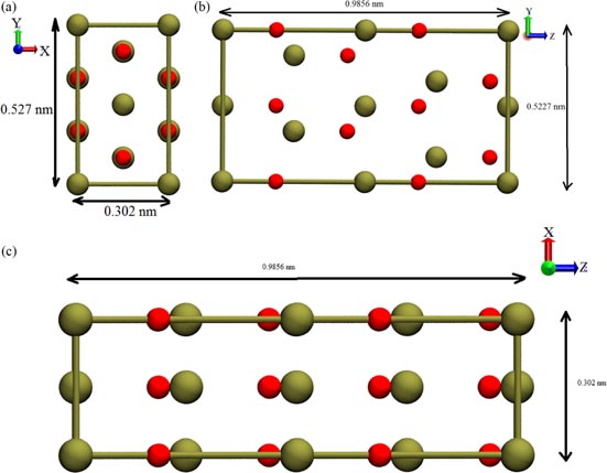
Figure 8. View of 4H–SiC on (a) view on XY plane, (b) view on YZ plane and (c) view on XZ plane.
Download figure:
Standard image High-resolution imageThe main engineering properties of β-SiC (3C–SiC) and α-SiC (6H–SiC and 4H–SiC) are compared in table 3, along with the corresponding values for single crystal silicon as a reference material. Table 4 lists the properties that are desirable in a material to produce an ideal optical mirror alongside indexing the properties of various commercially available mirror materials. It is evident from tables 3 and 4 that SiC exhibits superior engineering properties over other materials making it a preferred choice for such applications. Table 5 shows calculations of the critical crack length (which can be obtained by applying a simple empirical formula [57–59]), which suggest that single crystal 3C–SiC has the maximum fracture toughness and maximum hardness while 6H–SiC has the least hardness and shares the same fracture toughness as 4H–SiC.
Table 3. Engineering properties of polytypes of SiC compared with single crystal silicon [40].
| Parameter | 3C–SiC | 4H–SiC | 6H–SiC | Silicon |
|---|---|---|---|---|
| Experimental lattice parameter (Å) | a = 4.359 [41] | a = 3.079 [41] | a = 3.0817 [41] | 5.43 [42] |
| c = 10.254 [41] | c = 15.1183 [41] | |||
| Mechanical properties | ||||
| Bulk modulus (K) (GPa) | 225 [43] | 215 [44] | 215 [44] | 98 |
| Shear modulus (G) (GPa) | 124 [45] | 131.4 [45] | 131.4 [45] | 79.9 [46] |
| Hardness (H) on (1 0 0) plane (GPa) | 25–30 [44] | 26 [47] | 20–26 [48] | 9.8 [46] |
| Poisson's ratio (υ) | 0.267 | 0.231 | 0.231 | 0.27 [46] |
| Young's modulus (E) (GPa) 'E = 3K (1 − 2υ)' | 314.55 | 347.01 | 347.01 | 135.24 |
| Fracture toughness (MPa m1/2) (dependent on plane and direction) | 2.02 [49] | 1.9 [50] | 1.9 [50] | 0.9 [51] |
| 3.23 for CVD | ||||
| Electronic properties [31, 52–55] | ||||
| Band gap (eV) | 2.3 | 3.2 | 3 | 1.1 |
| Hole mobility (cm2 V−1 s−1) | 40 | 115 | 90 | 420 |
| Electron mobility (cm2 V−1 s−1) | 750 | // c-axis: 800 | // c-axis: 60 | 1200 |
| ⊥ c-axis: 800 | ⊥ c-axis: 800 | |||
| Thermal conductivity (W cm K−1) | 4.9 | 3–5 | 3–5 | 1.5 |
| Electron saturation velocity (cm s−1 × 10⁷) | 2.5 | 2 | 2 | 1 |
| Breakdown electric field strength (V cm−1 × 10⁶) | 1.8 | // c-axis: 3 | // c-axis: 3.2 | 0.6 |
| ⊥ c-axis: 2.5 | ⊥ c-axis: >1 | |||
Table 4. Properties of several different materials for application in optical mirrors [56].
| Properties | Density (ρ) | Young's modulus (E) | Thermal conductivity (k) | Fracture toughness | Knoop hardness |
|---|---|---|---|---|---|
| Units | Kg m−3 × 10⁻³ | GPa | W/mK | MPa m1/2 | Kg mm−2 |
| Desirable for mirror | LOW | HIGH | HIGH | HIGH | |
| Single crystal silicon | 2.33 | 147 | 150 | 0.9 | |
| Polycrystalline silicon | 2.33 | 130 | 150 | 15 | 1150 |
| α-SiC (Sintering) | 3.2 | 450 | 2.2 | 2.8 | 2740 |
| β-SiC (CVD) | 3.21 | 466 | 300 | 3 | 2450 |
| RB-SiC | 3 | 380 | 150 | 4 |
![$c\ast =120\left[ {\frac{K_{{\rm c}}^{2}}{H^{2}}} \right]$](https://content.cld.iop.org/journals/0022-3727/47/24/243001/revision1/jphysd492183ieqn001.gif)
1.4. Crystal anisotropy in SiC
The anisotropic variation in a material is believed to originate from the differences in the density of atoms on a particular crystal orientation and the distance between nearest neighbour atoms along a specific cutting direction [60]. This in turn influences the cutting mechanics (slip occurs on the densest plane and along the shortest direction) and the nature of the plastic deformation of the workpiece material. This is the perspective from a crystallographic point of view. There is also another view2 that the ductile/plastic response (thus slip, etc) is within the HPPT material, whereas the brittle/fracture response is within the atmospheric phase (influenced by stress state, tension/compression in particular) of the material.
In a diamond cubic lattice material such as 3C–SiC, the Burgers vector can be calculated as
 where a is the lattice parameter of 3C–SiC as 4.36 Å. 3C–SiC is a diamond cubic lattice material and hence studying its anisotropy is relatively simpler in comparison to other polytypes. In a recent study, Goel et al [61] have shown that the extent of anisotropy exhibited by 3C–SiC could be upto 44%. Experimental investigations on nanometric cutting of single crystal 6H–SiC have also shown an anisotropic variation in the cutting forces [62]. These observations point to the fact that the crystal orientation of the SiC work piece significantly impacts its cutting behaviour [63] and hence a properly selected crystal setup is an essential step in improving both the tool life and the attainable machined surface roughness. As is well known with other materials, nanometric cutting of SiC also involves plastic deformation ahead of the cutting tool and elastic recovery of the machined surface underneath the clearance face of the tool. Thus, the variation in the elastic modulus with crystallographic orientation tends to influence the machined surface finish, sub-surface integrity, and residual stresses on the finished surface.
Table 6 compares the Young's modulus of 3C–SiC along different crystallographic planes and shows that the maximum Young's modulus of 3C–SiC is on the (1 1 1) crystal orientation (557 GPa), while the minimum Young's modulus is on the (1 0 0) crystal orientation (314 GPa). To explore other features of SiC on crystallographic planes, Goel et al [61] calculated the number of atoms on a crystal plane, atomic density per unit area, minimum distance between atoms on a plane, and distance between two adjacent planes of 3C–SiC which are shown in table 7. It can be seen from table 7 that the atomic density per unit area in single crystal 3C–SiC is highest on (1 1 0) crystal orientation and the distance between the two adjacent planes is farthest compared to the other two orientations. Here only single crystal SiC is compared although CVD 3C–SiC is also found to exhibit a strong degree of crystal anisotropy and its details can be found elsewhere [7]. Crystal anisotropy of SiC is therefore an important variable in influencing its deformation, preferentially along certain combinations of crystallographic planes and directions, and is thus an important consideration during machining.
Table 6. Direction-dependent mechanical properties in single crystal 3C–SiC [61].
| 3C–SiC properties | Reference | Values |
|---|---|---|
| Elastic constant C11 | Experimental data [64] | 390 GPa |
| Elastic constant C12 | Experimental data [64] | 142 GPa |
| Elastic constant C44 | Experimental data [64] | 256 GPa |
| Young's modulus (E100) |
 |
314 GPa |
| Young's modulus (E110) |
 |
467 GPa |
| Young's modulus (E111) |
 |
557 GPa |
| Poisson's ratio |
 |
0.267 |
| Crystal anisotropy |
 |
0.436 |
Table 7. Variation in the properties of 3C–SiC with respect to various crystal orientations.
| Orientation | Number of atoms on the plane | Atomic projection area | Atomic density per unit area | Minimum distance between the two atoms lying on the same plane | Distance between two adjacent planes |
|---|---|---|---|---|---|
| Cube (1 0 0) |
 |
a × a = a2 | 2/a2 = 0.1052 | a/2 = 2.18 Å | a = 4.36 Å |
| Dodecahedron (1 1 0) |
 |
 |
 |
a/4 = 1.09 Å | 1.707a = 6.16 Å |
| Octahedron (1 1 1) |
 |
 |
 |
 |
0.577a = 2.514Å |
2. Diamond machining
2.1. Introduction to SPDT
Single point diamond turning (SPDT) is one of the most efficient ultra-precision material removal processes. It is capable of removing material at the scale of a few atomic layers to produce optical quality finished surfaces using a single point diamond-cutting tool. SPDT provides a machining form accuracy and machined surface finish that are among the best ranges obtained via a multitude of processes such as lapping and polishing [8]. Furthermore, SPDT offers flexibility of generated form, improved step-definition, deterministic form accuracy and economy of fabrication time and is the preferred ultra-precision manufacturing process range in terms of productivity and cost [65]. Currently, with the inclusion of Fast Tool Servo, Slow Tool Servo, fly cutting techniques or μ-LAM, SPDT can be used to machine freeform (non- rotationally symmetric) machined surfaces to fabricate SiC. In the early days of inception, SPDT was limited to machine soft metals like copper but rapid technological advancements have driven an expansion of the SPDT technology to machine brittle materials [66]. Based on the experimental trials of materials like germanium and silicon, the key discovery was that with careful selection of the process parameters, brittle materials can be machined in the 'ductile-regime'—where chip removal takes place by virtue of plastic deformation rather than by brittle fracture. The first mathematical approach for quantifying the key machining parameters of SPDT was developed by Scattergood et al [67], who highlighted the importance of the critical chip thickness [68] in the context of ductile-regime machining. However, an overall phenomenological understanding of the complex interplay of all aspects that effect tool wear and their dynamic influence on the ductile behaviour of brittle materials like SiC is still not developed. In this regard, this review aims to provide an atomistic-level understanding on the influence of the crystal structure of the workpiece material, sub-surface crystal deformation layer depth and on the phenomena involved in the tool wear mechanism. The next section explores the phenomena of the brittle–ductile transition (BDT) involved in the manufacturing of silicon carbide.
2.2. SPDT of brittle materials
It was as early as 1954 when the concept of plastic deformation of brittle materials was first acknowledged by King and Tabor [69] as a result of observations on frictional wear of rock salt. They observed that, although some cracks and surface fragmentation occurred during heavy abrasive wear, there was some plastic deformation involved. Similarly, Bridgman et al [70] recognized that a brittle material such as glass exhibited ductility under high hydrostatic pressure. Subsequently, Lawn and Marshall [58] proposed empirical relationships to relate the indentation load and observed crack length with the physical properties of the material such as fracture toughness and hardness, as follows:


where P is the indentation load, c is the observed crack length, Kc is the fracture toughness (resistance to fracture) of the substrate material, H is its hardness, which is a measure of plastic deformation, and λ0 and μ0 are geometrical constants dependent on the indenter shape.
The fracture toughness of diamond cubic crystal structured materials, such as in silicon and 3C–SiC, has been suggested to follow the following relationship [71]:

where a0 is a constant, G and E are the shear and Yang's elastic modulus and υ is Poisson's ratio.
Further developments on machining brittle materials in the ductile-regime led to the identification of the critical indent size (CIS) [59] expressed as follows:

The identification of the elastic-plastic response of brittle materials primarily during their nanoindentation revealed that almost any material, including super-hard substances like diamond and SiC, can be deformed plastically even at low temperatures [72] under the influence of large hydrostatic stresses. Subsequently Ikawa and co workers [73–78] proposed a model of the BDT by considering the forces that give rise to slip and cleavage. They suggested that plastic deformation occurs underneath the indenter when the resolved shear stress exceeds a certain critical value in the direction of the shear plane, whereas cleavage takes place if the resolved tensile stress exceeds a certain critical value in the direction normal to the cleavage plane. They also reported that the critical values of stress for plastic deformation and cleavage are also governed by the density of lattice defects and dislocations present in the work material (which exist in all practically available materials). With smaller indent depths, the size of the resulting critical stress field is small enough to avoid cleavage initiated at the defects, but, with larger indent depths, the larger critical stress field allows for sufficient nuclei for crack propagation, which initiates from defects within the material. It was thus realized that it is possible to machine brittle materials using appropriate machining parameters, but at a very fine scale of several micro or nanometres. The execution of such a machining process on brittle materials, where the chips are generated through plastic deformation rather than fracture, is known as 'ductile-regime machining.' In the late 1990s, Blake and Scattergood [67] suggested that a critical chip thickness (tc) separates the regime of plastic deformation from brittle fracture material removal. Accordingly, they proposed a new machining model to explain the ductile-regime machining of brittle materials as shown in figure 9.
Figure 9. Ductile-regime machining (a) analytical model (2D representation of the 3D condition showing nose radius of the tool [66]. Reprinted with permission from [68], Copyright 1991 Elsevier. (b) MD model (2D model showing cutting edge radius).
Download figure:
Standard image High-resolution imageFigure 9 illustrates the horizontal distance between the critical chip thickness and the cutting tool nose centre denoted here by Wd (sometimes denoted as Zeff), which is an important parameter in the diamond machining process. For an SPDT operation, undesirable fracture damage is assumed to initiate at the critical chip thickness (tc), which propagates up to a depth, Yc. The critical crack length (Yc) is of particular importance as it varies along the nose radius according to the feed rate of the tool. As shown schematically in figure 10, the crack does not penetrate below the subsurface damage at smaller feed rates and hence does not affect the final machined surface. However, as the feed is increased, Yc moves towards the machined surface and thus cracks begin to propagate into the final cut surface (i.e. the machined surface begins to show undesirable brittle fractures). As long as the fracture damage does not penetrate to the final machined surface, ductile-regime machining can be executed consistently. Notably, the fractured material in the remaining region of the uncut shoulder is carried away by the tool in the succeeding passes. It may be noted that the critical chip thickness tc represents the condition for any fracture initiation, whereas Yc is an indicator of the average depth of fracture propagation. Both these parameters are interdependent, and interact in a non-linear fashion that depends primarily on the state of the stress in the cutting zone.

Figure 10. Schematic for diamond turning at a (a) low feed rate and (b) high feed rate.
Download figure:
Standard image High-resolution image2.3. Machining forces during diamond machining
Figure 11 shows schematically the main parameters affecting the process of the nanometric cutting especially during machining of anisotropic brittle materials such as SiC. As shown in the bottom panel of figure 11, two coplanar forces (namely, the tangential cutting force (Fc or Fx) and the thrust force (Fy or Ft)) acting on a cutting tool fundamentally govern the cutting action of the tool. The third component shown, thrust force, Fz, acts in the direction orthogonal to the X and Y planes. Thrust force mainly influences surface error, as it tends to push the tool away from the workpiece while the tangential force causes displacements in the direction of cut chip thickness and its variation therefore relates to chatter. The cutting or machining forces are by far the most tangible indicators used to characterize any machining process.

Download figure:
Standard image High-resolution imageAn experimental measurement of the cutting forces obtained from the machining trials on single crystal 6H–SiC along several crystallographic orientations is shown in figure 12. The regions of ductile-brittle cutting correlate to the sample crystalline structure, i.e. there are six regions of ductile and brittle behaviour (six transitions) that match the sixfold coordination of 6H SiC. The high force peaks are believed to arise either due to the ductile machining conditions and/or from higher material property values in the crystal orientations at these locations. Similarly, the low forces (valleys) are due to brittle material removal and/or lower material property values at these locations. Furthermore, not only the cutting forces are an important indicator for the assessment of local machining conditions, the magnitude and variation in the cutting forces is also found to be of use to distinguish ductile-regime cut from brittle regime cut in SiC as shown in figure 13. Knowledge of cutting forces from simulation and/or from the experiments during mechanical based machining is therefore an important indicator to characterize the process of material removal especially during ductile-regime machining of brittle materials.

Figure 12. Cutting force data obtained during cutting of 6H–SiC at 100 nm depth of cut. Reprinted from [7] courtesy of J Patten.
Download figure:
Standard image High-resolution image
Figure 13. Cutting force and acoustic emission data to distinguish brittle-regime with ductile-regime machining. Reprinted courtesy of J Patten.
Download figure:
Standard image High-resolution image2.4. Influence of cutting tool geometry
2.4.1. Rake angle and clearance angle.
It has been demonstrated that material removal at extremely fine depths of cut to remove certain atomic layers of material involves a high coefficient of friction that is dependent solely on the tool rake angle and is independent of the thrust force or normal force (Ft) on the cutting tool [81]. During the condition when the uncut chip thickness is equal or lesser than the cutting edge radius of the tool, rake angle appears to determine both the direction and the magnitude of the resultant cutting force. The use of a negative rake angle tool for ductile-regime machining of brittle materials has become somewhat of a conventional practice for the machining of brittle materials [82, 83]. A schematic comparison of the cutting process using negative and positive rake angle tools is shown in figure 14.

Figure 14. Difference in the force vector and stress distribution due to positive and negative rake angles where lc is the length of contact between cutting tool and chip. Reprinted with permission from [84], Copyright 2010 Springer.
Download figure:
Standard image High-resolution imageIt can be seen from figure 14 that the tangential force acts along the wedge of the cutting tool so that the normal force acts onto the wedge face. Along these directions, the shear stress and compressive stress on the cutting tool varies during the course of machining. When positive rake angles are used, the normal force exerts a bending stress on the cutting tip of the tool under which diamond, being extremely brittle, might eventually chip off. When a negative rake-angled cutting tool is used, this bending effect does not occur because it is replaced by compression on the cutting tool. Additionally, a negative rake angle cutting tool is thought to exert a hydrostatic stress state in the workpiece, which inhibits crack propagation and promotes a ductile response from brittle materials during their nanometric cutting [73, 85]. Nakasuji et al [73] noted that the effect of rake angle in cutting is analogous to that of the apex angle of an indenter: low angles of approach result in relatively small hydrostatic stress fields which, in turn, enable ductile regime machining. Negative rakes of approximately −25° to −45° with clearance angles of approximately 8°–12° are recommended for improved performance of the SPDT process [86]. The reason for such a selection is that a high clearance angle reduces rubbing while a corresponding increase in rake angle provides mechanical strength to the wedge of the cutting tool [87]. It may be noted here that when the depth of cut is smaller than the edge radius, an effective rake angle is presented by the tool [88]. In such cases, a 0° rake angle tool already presents some negative rake and, indeed, has been found to provide a better finish than −25° or −30° rake angle tools. Rake angle calculation can be used to relate cutting edge radius as shown in figure 15:

R is the tool nose radius, d is the depth of cut and γ is the effective rake angle.
Figure 15. Schematic diagram showing effective rake angle.
Download figure:
Standard image High-resolution image2.4.2. Influence of cutting tool edge radius.
A tool with a very sharp edge may wear out quickly because of stress concentration or break, chip, i.e. fracture; hence a finite edge radius is always preferred. Additionally, when the uncut chip thickness is less than the tool cutting edge radius, the thrust force increases more rapidly than the tangential cutting forces [89]. Griffith's criterion suggests that the propagation of brittle fracture involves the balance between the absorption of volumetric strain energy and the release of surface energy, i.e. the energy required for plastic deformation is directly proportional to the volume of the material removed whereas the energy for brittle fracture is directly proportional to the cracked surface area [7]. The process of machining brittle materials can thus be treated in terms of the minimum energy i.e. the BDT transition can be determined as the condition at which it will take more specific cutting energy to execute ductile-regime machining than it takes to execute brittle-fracture dominated machining. In a model using this approach [90], the consumption of energy involved during the machining of brittle materials was described as a function of the properties of the workpiece material, tool geometry and process parameters. Bifano et al [91] suggested that at smaller feed rates the energy required to propagate a crack is greater than the energy required for plastic yielding and hence plastic response of brittle materials prevails. Moreover, theory of plasticity suggests that the magnitude of hydrostatic stress determines the extent of plastic deformation prior to fracture, which in turn, determines the material's ductility. Therefore, when the tool edge radius in the cutting region generates sufficient hydrostatic pressure, plastic deformation is more likely to occur rather than crack generation, even at a lower temperature. Therefore, ductile mode cutting of brittle materials can be achieved. The above proposition is considered to be the classical theory of the brittle to ductile transition in diamond turning. Indeed it has been cited [92] as a main reason for the cutting edge radius requirement on the diamond cutting tools rather than sharp-edged tools as shown in figure 16.

Figure 16. Schematic illustration of the influence of the edge radius on SPDT. Reproduced with permission from [92]. Copyright 2002 Elsevier. (a) Brittle regime and (b) ductile regime.
Download figure:
Standard image High-resolution imageAnother reason that hard, brittle materials exhibit ductility at nanoscale could potentially be the fact that at nanoscale, pre-existing defects are relatively rare, and therefore there are few stress concentrators that could lead to crack initiation and fracture and thus plastic deformation becomes dominating primarily via high pressure phase transformation (HPPT) [93] and/or dislocation nucleation [14, 94–96]. Providing an edge radius on the cutting tool thus causes two particularly significant phenomena [85, 97, 98]:
- Edge roundness decreases the stress concentration and produces a hydrostatic stress field in the cutting region and minimized crack opening (by suppressing the crack).
- The effective rake angle caused by the small radius becomes large and negative and, as a result, material in front of the cutting edge is pushed downward and compressive stresses (a hydrostatic stress field) become dominant.
For semiconductors, a strong correlation was found between nano-indentation hardness and metallization pressure [99, 100]. The metallization pressure (Herzfeld–Mott transition [101]) is the value under which brittle semiconducting materials become metallic (i.e. the band gap vanishes because of the closure of the valence-conduction band gap due to the overlap of wave functions and the subsequent delocalization of the valence electrons). This process is facilitated by HPPT which has been demonstrated to be an outcome of the shear strain rather than simple hydrostatic strain (i.e. predominance of bond-bending over bond-stretching) [102]. Gilman [99–101] suggested that it is the change in bond angle rather than a change in bond length that appears to cause the metallization of semiconductors, as observed during diamond polishing process as well [103]. He explained that in a diamond cubic lattice, bond length could only bring about a change in volume, not necessarily shape; whereas a change in bond angle can change both shape and volume. This mechanism has already been realized to be plausible for silicon [38] but is yet to be experimentally verified in SiC.
2.4.3. Influence of undeformed chip thickness.
Recently, Patten and co-workers have examined the critical depth of cut at which the ductile to brittle transition (DBT) occurs. Using common machining parameters, they identified critical depths for several materials as shown in table 8. With a large nose radius cutting tool, they reported that 4H–SiC exhibits DBT depth of up to 820 nm [104] whereas the DBT depth of polycrystalline 3C–SiC (CVD) was found to be 550 nm [105].
Table 8. DBT depth obtained for several brittle materials [7].
| Materials tested | Average ductile-brittle transition depth (nm) |
|---|---|
| 4H–SiC (single crystal) | 20 |
| 6H–SiC (single crystal) | 17.5 |
| 3C–CVD–SiC (polycrystal) | 42.5 |
| Silicon (single crystal) | 185 |
| Sapphire | 122.5 |
| Quartz | 87.5 |
| Spinel | 205 |
It may be noted that these depths are good only as a reference to relate the brittleness of the materials with each other because DBT is dependent on the geometry of the cutting tool. In order to reduce the number of these parameters, an indicator, critical undeformed chip thickness is found to be of importance. One way of obtaining critical chip thickness is by using the empirical relations as shown in table 9.
Table 9. Calculation of critical chip thickness in 6 H–SiC.
| S.NO. | Material properties | Unit of measurement | Values |
|---|---|---|---|
| Fracture toughness (Kc) | MPa.m1/2 | 1.9 | |
| Hardness (H) | GPa | 22 | |
| Elastic modulus (E) | GPa | 347.01 | |
| 1 | Critical crack length | µm | 0.895 |
 |
|||
| 2 | Critical chip thickness | µm | 0.01764 |
 |
Another way of assessing the critical chip thickness is by examining the uncut shoulder experimentally as shown in figure 17 [36]. Using figure 17, one can use the mathematical expression obtained by Scattergood et al [68] to correlate the critical chip thickness with respect to the nose radius of the cutting tool and the extent of the BDT in 6H–SiC was obtained as

Comparing the two measurements (experimental and empirical), it may be seen that the experimental value was found to vary only slightly with the predicted value of critical undeformed chip thickness for 6H–SiC and is only in the range of few nanometres which is quite difficult to harness in reality during the experiments. Thus, the commercial realization of SPDT of SiC is still a long way off in reality [106]. Nevertheless, attempts to demonstrate technical feasibility and explore the possibility of execution of SPDT of SiC have already been initiated. Some of these early attempts include machining of 3C–CVD–SiC and a machined surface roughness of Ra value of 83 nm was obtained [107]. Similarly, using a coolant of the copper nanoparticles in the form of a grease, SPDT was used to generate a very fine machined surface roughness of Ra value 14 nm on RB-SiC and it dropped to 23 nm while dry cutting [108] indicating the importance in the chemistry of the coolant (such as in CMP) during the cutting process. However, more efforts are needed to understand the ductile-regime machining of SiC. A possible approach may be to use molecular dynamics (MD) simulation which has previously been used to successfully understand a range of mechanical engineering phenomena.

Figure 17. Measured uncut shoulder of diamond turned 6H–SiC. Reprinted with permission from [36], Copyright 2013 Elsevier.
Download figure:
Standard image High-resolution image3. MD simulation of machining processes
Figure 18 summarizes the modelling efforts in order to understand the complex nature of machining processes. The model includes cutting parameter, tool geometry and material considerations. Most of these models calculate fundamental physical variables (stage I) which are then used to understand the machining performance (stage II). This algorithm can be used by adapting any suitable simulation approach such as finite element analysis, smooth particle hydrodynamics or MD simulation. MD is a scientific algorithm through which an assemblage of atoms and/or molecules is given prescribed intermolecular interactions for a specified period of time to yield a trajectory of their movement. The principle of MD was based on the notion that Newton's second law of motion is valid even at the atomic level. The implementation of MD simulation was first developed through the pioneering work of Alder and Wainwright in the late 1950s [110] in their study of the interactions of hard spheres. Since then, a number of studies have emerged to study machining processes using MD simulations. MD is particularly useful to understand the ductile-regime machining of SiC because the extent of ductility offered by SiC is in the range of few nanometres. Therefore, MD is a productive phenomenological tool for understanding discrete processes such as the effect of the crystal structure of the material (cutting tool and the workpiece), high-pressure phase transformation, wear of cutting tools occurring during diamond machining of SiC. In order to carry out an appropriate MD simulation, it is important to understand the importance of potential energy function which must include aspects of HPPT to simulate both ductile and brittle phase machining.
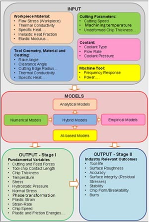
Figure 18. Two stage modelling approach for machining processes. Reprinted with permission from [109], Copyright 2013 Elsevier.
Download figure:
Standard image High-resolution image3.1. Potential energy function
MD simulation requires a constitutive description of the terms basis which atoms in a simulation interact with each other. This interaction is governed by a potential energy function that roughly accounts for quantum interactions between electron shells and represents the physical properties of the atoms being simulated, such as its elastic constants and lattice parameters. While the newly developed formalisms of the potential energy functions are providing greater accuracy, they are sometimes computationally very expensive. This is shown and plotted in figure 19 and table 10.
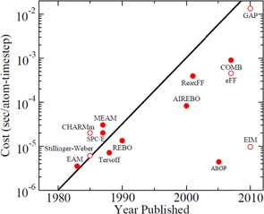
Figure 19. Single CPU cost in seconds/atom/time step for various potential functions (the black line represents a doubling in computational cost every two years, akin to Moore's Law for hardware complexity [111]).
Download figure:
Standard image High-resolution imageTable 10. List of potential functions with respect to the time of introduction.
| S.No. | Year | Name of the potential function | Materials suited |
|---|---|---|---|
| 1 | 1984 | EAM: embedded-atom method [112] | Cu |
| 2 | 1985 | Stillinger-Weber potential [113, 114] | Si |
| 3 | 1987 | SPC: simple point charge [115] | H2O |
| 4 | 1988 | BOP: bond order potential | |
| 1988 | • Tersoff-1 variant for silicon [116] | Si | |
| 1989 | • Tersoff-2 for better elastic properties of silicon [117] | Si | |
| 1990 | • Tersoff-3 for silicon, germanium and carbon [118, 119] | Si, Ge and C | |
| 1994 | • Tersoff-4 for silicon and carbon [120] | Si and C | |
| • Tersoff-5 for amorphous silicon carbide [121] | SiC | ||
| • Refinements in Tersoff potential function [122–124] | Si and C | ||
| 5 | 1989 | MEAM: modified embedded-atom method [125] | Si and Ge |
| 6 | 1990 | REBO: reactive empirical bond order [126] | Carbon |
| 7 | 2000 | AIREBO: adaptive intermolecular reactive empirical bond order [127] (4 body potential function) | Hydrocarbons and Carbon |
| 8 | 2001 | ReaxFF: reactive force field [128] (Capable of bond breaking and bond-formation during the simulation) | Universal |
| 9 | 2005 | ABOP: analytical bond order potential [64] (3 body potential function) | Si and C |
| 10 | 2007 | COMB: charge optimized many-body [129] | SiO2, Cu, Ti |
| 11 | 2008 | EIM: Embedded-ion method [130] | Ionic e.g. NaCl |
| 12 | 2010 | GAP: Gaussian approximation potential [131] | Universal |
| 13 | 1998–2001 | Other important potential functions relevant in contact loading problems [132–134] | Si, B and N |
Much of the research done in the past on simulating contact loading processes has made use of Morse potential function which is a pair potential. Unlike Morse potential functions, many of the potentials used in physics, such as those based on bond order formalism, may describe both bond breaking and bond formation (e.g., Tersoff is a three-body potential function, while the AIREBO function is a four-body potential function). The Tersoff formalism or, more appropriately, the 'Tersoff-Abell' formalism is the most widely used bond order potential (BOP) formalism. Tersoff based his potential on an idea presented by Abell a few years earlier on BOP, which has environmental dependence and no absolute minimum at the tetrahedral angle. Tersoff functions gained wide popularity in the 1990s for MD simulations. However, one key drawback of this potential function is that it describes the graphite-to-diamond transformation rather poorly. However, it has been noted that simply increasing the parameter S in the potential to 2.46 Å improves this aspect [135]. Tersoff functions are also known to poorly predict the melting point of silicon, which was later refined by an adjustment of three parameters of this potential [122]. To overcome another limitation of the poor description of the dimer properties of silicon by Tersoff, another potential function has been proposed that is an analytical bond order potential (ABOP) of almost the same formalism [64]. Overall, Morse potential functions limit the exploration of interaction within atoms of the workpiece and the cutting tool; while Tersoff potential functions have limitations in accurately describing the thermal aspects which might limit the study of some machining processes related to high temperature applications. Although there have been many refinements in the development of BOP functions, a common limitation of all these potential functions is that they are short ranged and only represent ductile behaviour rather than the brittle behaviour of SiC. Consequently, study of mechanisms of fracture, wear, and plasticity is somewhat constrained by these potential functions. In an attempt to address this gap, a recent effort has been made by decoupling the condition for a nearest-neighbour relationship from the range of the potential [136]. Subsequent refinements have led to a formalism, which is developed by using the screening functions to increase the range of these potentials [137]. By changing the cut-off procedure of all the bond order potential functions, screening function has been reported to reproduce an improved description of amorphous phases and brittle behaviour of silicon, diamond and silicon carbide. Further details are presented by Pastewka et al [138] in the form of a review, explicitly highlighting some of the important considerations needed to use a potential energy function to model phenomena, such as fracture, wear or plasticity in materials like silicon, carbon and silicon carbide.
4. Our understanding of ductility in silicon carbide using MD and experiments
HPPT is known to induce the Herzfeld–Mott transition, which causes the metallization of brittle materials during their nanometric cutting. This research area is now emerging as a new field of knowledge and is being referred to as High Pressure Surface Science [106]. Unlike silicon, the ductile response of silicon carbide has not been studied much. In the literature which is published so far, there is considerable incongruence on the cause of ductility of silicon carbide. Earlier studies on the ductility of SiC suggested that 3C–SiC undergoes a phase transformation from its stable structure to a β-tin structure [139] while later studies suggested direct amorphization of 3C–SiC [140, 141] or its transformation from its stable zinc-blende lattice structure to a rocksalt structure [43, 142, 143]. Similarly, 6H–SiC and 4H–SiC have been reported to transform to a polycrystalline phase [144], exhibiting no HPPT [108, 145], or dislocation nucleation followed by propagation within the zinc-blende phase [146].
An experimental study revealed that the rocksalt structural transformation in 3C–SiC requires a transformation pressure of 100 GPa [145] against numerically predicted values of 64.9 GPa [140] and 66 GPa [147]. In contrast, the first machining trial on SiC reported a cutting pressure [62, 148] lower than the predicted value of 60 GPa based on the Herzfeld's theory [99]. Gust et al [149] reported an observation of phase transformation in SiC at a pressure of about 24 GPa which was contradicted by the Hugoniot data of Vogler et al [150] who showed a transformation to take place at a pressure of about 104 GPa with an associated volume change of about 9%.
Sekine et al [39] noticed that a phase transformation in 6H–SiC begins from 105 GPa and ends at 137 GPa with an associated volume reduction of upto 15% (figure 20). In addition to the above observations, researchers have also used Raman spectroscopy to investigate the ductile response of SiC particularly during the ductile-regime machining which is discussed next.

Figure 20. Hugoniot data for 3C–SiC (C1 and C2 bars represent transformation of the zinc blende structure to rocksalt structure at about 66 GPa obtained from ab initio pseudo-potential calculations, while the Y1 and Y2 bars also represent the same transition but at a higher pressure of about 105 GPa obtained from experiments. Reprinted with permission from [39]. Copyright 1997 The American Physical Society.
Download figure:
Standard image High-resolution image4.1. Laser Raman spectroscopy
Ravindra [7] deployed Laser Raman spectroscopy to study and investigate the occurrence of phase transformation in SiC arising out of the cutting conditions during SPDT of SiC. The Raman spectra obtained by them before and after machining of single crystal 6H–SiC, single crystal 4H–SiC and polycrystalline 3C–SiC (CVD) are shown in figure 21, figure 22 and figure 23, respectively. In addition to conventional machining, they also performed machining trials by supplying external heat through a transparent diamond to the pressurized material using a laser and this was referred to as micro-laser assisted machining (μ-LAM) [151]. The spectra of the machined chips after μ-LAM are also compared in figures 22 and figure 23 along with the spectra of pristine specimens. Interestingly, machined chips obtained from μ-LAM and normal machining both showed amorphous remnants. However, the intensity of the amorphous characteristics obtained for the LAM machining was noticeably much higher (broader peaks) than the chips machined under room temperature with three new peaks (495, 755 and 915 cm−1) appearing due to the thermal effects. Except for the amorphous broadening, no appreciable changes were observed in the Raman spectra for the machined and unmachined specimens. Therefore, Raman spectroscopy did not reveal any instantaneous changes in the structure of SiC (as the surface may recrystallize upon post process heating) as the ibid. speculated that back transformation of the pressure could have resulted in the amorphous remnants.
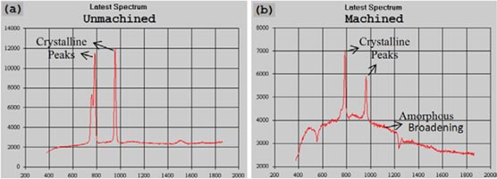
Figure 21. Laser Raman spectrum of an (a) unmachined and (b) machined 6H–SiC surface [7].
Download figure:
Standard image High-resolution image
Figure 22. Laser Raman spectrum of a 4H–SiC surface. (a) Machined surface, (b) cutting chips. Reprinted from [7] courtesy of J Patten.
Download figure:
Standard image High-resolution image
Figure 23. Laser Raman spectrum of an (a) unmachined and (b) machined 3C–SiC (CVD) surface. Reprinted from [7] courtesy of J Patten.
Download figure:
Standard image High-resolution image4.2. Other studies on ductility of SiC
There are several other studies which report response of SiC under a variety of different contact loading conditions (table 11 and table 12).
Table 11. Previous studies on hexagonal SiC under different contact loading conditions.
| Material | Author, Year | Process studied | Conclusions on the ductility of hexagonal SiC |
|---|---|---|---|
| 4H–SiC | Hong et al 1999 [152] | Compression | Deformation induced dislocation on the (0 0 0 1) basal plane with a Burgers vector depending on the deformation temperature i.e. above 1373 K, the dislocation (Burgers vector
 dissociates into two dissociates into two
 partials while at temperatures between 823 K to 1373 K, single leading partials drag stacking fault behind them. partials while at temperatures between 823 K to 1373 K, single leading partials drag stacking fault behind them. |
| 4H–SiC | Demenet et al 2000 [153] | Compression | Nucleation and glide of single partial dislocations below a critical temperature of 1373 K and formation and glide of dissociated dislocations above 1373 K. |
| 4H–SiC | Schuh et al 2004 [154] | Nanoindentation | Stress assisted, thermally activated defect nucleation |
| 6H–SiC | Patten et al2005 [62] | Nanometric cutting | High pressure phase transformation of SiC |
| 6H–SiC | Yan et al 2010 [144] | Nano-indentation | Transformation to a polycrystalline phase |
| 6H–SiC | Levitas et al 2012 [155] | Rotation diamond anvil cell | Transformation to a high-density amorphous (hda) phase |
| 4H–SiC | Demenet et al 2013 [156] | Nanoindentation | Nucleation and glide of non-dissociated perfect dislocations (no stacking faults and no dissociated dislocations) |
Table 12. Previous studies on cubic SiC under different contact loading conditions.
| Material simulated | Author, Year | Process studied | Conclusions on ductility of SiC |
|---|---|---|---|
| 3C–SiC | Yoshida et al 1993 [145] | Pressure loading | No high pressure phase transformation (HPPT) |
| 3C–SiC | Tang, 1995 [140] | Nano-scratching | Shear instability induced amorphization |
| 3C–SiC | Shimojo et al 2000 [43] | Pressure loading | Rocksalt structural transformation |
| 3C–SiC | Szlufarska et al 2005 [141] | Nano-indentation | Amorphization of SiC |
| 3C–SiC | Noreyan et al 2005 [142] | Nano-scratching | Rocksalt structural transformation |
| 3C–SiC | Szlufarska et al 2009 [146] | Nano-indentation | Dislocation nucleation within the zinc-blende phase without any HPPT |
| 3C–SiC | Zhao et al 2011 [157] | Nano-indentation | Shear slip |
| 3C–SiC | Goel et al 2012 [61, 102, 158] | Nanometric cutting | sp3–sp2 disorder of SiC |
| 3C–SiC | Demenet et al 2013 [156] | Nano-indentation | Nucleation and glide of perfect dislocations (no stacking faults and no dissociated dislocations) |
Interestingly, while the response of silicon is found to be the same under all sorts of contact loading conditions, this is not the case with SiC as can be seen from this table 11 and table 12. Recently, grain boundary (g.b.) analysis in conjunction with large angle convergent beam electron diffraction (LACBED) was used to propose that dislocations in 4H–SiC were observed to be in the basal plane with their Burgers vector as 1/3〈 − 1 − 1 2 0〉 [156]. For brittle materials like SiC, there may be two types of defect nucleations: dislocations or micro-cracks. Also, there are two kinds of cracks observed in a crystal i.e. basal-plane cracks (basal plane is the easy cleavage plane in 6H–SiC) and prism-plane cracks (associated with dislocations belonging to the secondary slip system).
Also, perfect dislocations in 4H–SiC were proposed to dissociate into Shockley partials as per the following reaction:

Further differences highlighted between hexagonal SiC, diamond cubic SiC and silicon are their slip planes [159]. In 3C–SiC, there are four different slip planes parallel to the (1 1 1) orientation whereas in hexagonal lattices (4H–SiC and 6H–SiC), there is only one set of slip planes which is parallel to the (0 0 0 1) orientation. Also, the primary cleavage plane in 3C–SiC is (1 1 1) whereas for 4H–SiC and 6H–SiC the cleavage plane is
 . Despite these differences, a common feature of all these three types of SiC are the three slip directions in each of the slip planes, parallel to
 and
and
 directions respectively. Therefore, it is much easier to activate one of the twelve slip systems along
(1 1 1) in 3C–SiC than one of the three
(0001) slip systems in 4H–SiC or 6H–SiC. Niihara [72] investigated and reported that the active slip systems in 6H–SiC are
directions respectively. Therefore, it is much easier to activate one of the twelve slip systems along
(1 1 1) in 3C–SiC than one of the three
(0001) slip systems in 4H–SiC or 6H–SiC. Niihara [72] investigated and reported that the active slip systems in 6H–SiC are

 near room temperature and (0 0 0 1)
at about 1173 K, which suggest that 6H–SiC will show a transition from brittle behaviour to plastic behaviour beyond this temperature. Fujita et al [160] and Maeda et al [161] examined dislocations in 6H–SiC and concluded that at temperatures above 1273 K, plastic deformation occurred by the movement of dislocations along (0 0 0 1)
near room temperature and (0 0 0 1)
at about 1173 K, which suggest that 6H–SiC will show a transition from brittle behaviour to plastic behaviour beyond this temperature. Fujita et al [160] and Maeda et al [161] examined dislocations in 6H–SiC and concluded that at temperatures above 1273 K, plastic deformation occurred by the movement of dislocations along (0 0 0 1)
 setup thereby confirming the earlier findings of Niihara. Riviere et al [162] suggested
 as the cross slip plane in 4H–SiC. It must be noted here that the
 plane in 4H–SiC is equivalent to
 plane in 6H–SiC. Experiments helped to recognize
$](https://content.cld.iop.org/journals/0022-3727/47/24/243001/revision1/jphysd492183ieqn029.gif) as the easy glide system in α-SiC while
as the easy glide system in α-SiC while
}$](https://content.cld.iop.org/journals/0022-3727/47/24/243001/revision1/jphysd492183ieqn030.gif) was recognized as the secondary slip system [163]. In 3C–SiC, it was proposed that the plastic deformation occurs by dislocation nucleation and glide on closely packed (1 1 1) planes [164]. Extant literature also shows that Pirouz et al [165] proposed a model where a partial glide dislocations mechanism was proposed and 4H → 3C type polytypic phase transformation was observed.
was recognized as the secondary slip system [163]. In 3C–SiC, it was proposed that the plastic deformation occurs by dislocation nucleation and glide on closely packed (1 1 1) planes [164]. Extant literature also shows that Pirouz et al [165] proposed a model where a partial glide dislocations mechanism was proposed and 4H → 3C type polytypic phase transformation was observed.
Of further interest is that simple compression differs from hydrostatic pressure [166] as it may have a component of deviatoric stress which can cause shear induced metallization via changes in bond angle [101]. The fact where SiC differs from silicon is due to the chemical ordering effect between the silicon and carbon atoms within SiC. Moreover, the moving line contact between the tip of the cutting tool and the workpiece during nanometric cutting differs from the point/planar contact during nano-indentation [167], so nanometric cutting conditions result in an increased energy transfer compared with the nano-indentation process. Yin et al [33] obtained the threshold indentation load for nanoindentation of 6H–SiC using a Berkovich indenter to be about 660 mN. From the ductile-regime machining experiments on 6H–SiC, a completely ductile surface was obtained for a cutting depth of 50 nm in contrast to cutting at a depth of cut of 500 nm which produced an entirely brittle behaviour [168]. This ductile response is also suggested to vary with the tool rake angle, cutting speed, crystal orientation, cutting edge radius and depth of cut etc [36]. This indicated that in contrast to a blunted geometry or an indenter with finite edge radius, point contact induces rapid conditions of non-hydrostatic stress, which can influence the ductile transition. A noticeable study in this regard comes from the experimental observation of Han et al [169] who reported an observation of large strain plasticity during bending of SiC nanowire at room temperature. They observed that the atomic slip in SiC occurs by gliding or shuffling on the
 planes based on the fact that the
plane has a favourable Schmidt factor with respect to the direction of the applied external force. Based on the TEM examination (figure 24), they observed multiple dislocations forming on the
plane with Burgers vector along [1 2 1] (also possible is a projection of
planes based on the fact that the
plane has a favourable Schmidt factor with respect to the direction of the applied external force. Based on the TEM examination (figure 24), they observed multiple dislocations forming on the
plane with Burgers vector along [1 2 1] (also possible is a projection of
![$[1\,0\overline {\,\,1} ]$](https://content.cld.iop.org/journals/0022-3727/47/24/243001/revision1/jphysd492183ieqn032.gif) direction and on the
direction and on the
 plane with a Burgers vector along [2 1 1] (or the projection of the [1 1 0] direction). Their observation reveals a simultaneous occurrence of metal-like dislocation interactions, lattice disordering and amorphization in SiC. Consequently, the scale effect was observed by them to bring ductility in SiC via a different route in addition to the classically proposed mechanisms as the process of increased dislocation density at an early stage, followed by an obvious lattice distortion, and finally reaches an entire structure amorphization while the sp3 bonding is conserved.

Figure 24. An area examined during the bending of the SiC nanowire showing formation of dislocations and the process of amorphization. The white dashed lines show the bent lattice by an angle of 19°. The bottom left part shows dislocations on the
 plane while the bottom right part shows the dislocations on the
plane. Reprinted with permission from [169], Copyright 2007 American Chemical Society.
plane while the bottom right part shows the dislocations on the
plane. Reprinted with permission from [169], Copyright 2007 American Chemical Society.
Download figure:
Standard image High-resolution imageMishra et al [164] used MD to simulate nanometric cutting of SiC and observed purely a elastic regime without any dislocations when the depth of the cut was less than 0.5 nm. On the other hand, at depths of about 1.5 nm they observed that the dislocation activity occurs by glide and cross slip, whereas at depths as high as 3.5 nm, V-shaped dislocation half loops were observed. However, unlike their work where only two directions were simulated, Goel et al [61] showed other directional dependencies of dislocation movement in 3C–SiC. They found that the volume of cleavage on a (1 1 1) orientation was observed to be far higher in comparison to other crystal setups, which is indicative of the fact that cleavage is dominant in 3C–SiC on this orientation irrespective of the cutting direction. This has been shown in figure 25 in addition to highlighting the mechanism of deformation of 3C–SiC along several other combinations of crystallographic orientations and cutting directions. In figure 25, atoms are coloured as per the scheme: green/red atoms are silicon and carbon atoms forming the crystalline 3C–SiC structure, Cyan atoms are the mixture of both Si and C atoms that have undergone structural transformation and have lost the pristine diamond cubic lattice structure while dark blue atoms belong to diamond cutting tool.
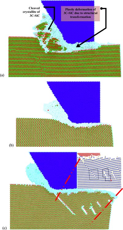
Figure 25. Snapshots from the nanometric cutting simulation in different combinations of crystal orientation and cutting directions [61, 80]. (a) Crystal setup 1: crystal orientation (1 1 1) cutting direction 〈−1 1 0〉, (b) crystal setup 4: crystal orientation (1 1 0) cutting direction 〈0 0 1〉, (c) crystal setup 5: crystal orientation (0 0 1) cutting direction 〈−1 1 0〉 (partial and perfect dislocations highlighted).
Download figure:
Standard image High-resolution imageUsing the discrete dislocation algorithm (DXA) [170–173], they showed the Burgers vector (table 13) of the observed dislocations in nine different combinations of crystallographic orientations. Eventually, they noticed that the dislocations (which were observed only in few cases) were of sufficiently smaller length to cause any glide or shuffle in 3C–SiC. Hence, the ductility observed was not on account of these dislocations but was attributed to the structural transformation in 3C–SiC.
Table 13. Identified Burgers vectors [61].
| Crystal setup | Crystal orientation | Cutting direction | Burgers vector |
|---|---|---|---|
| 1 | (1 1 1) | 〈−1 1 0〉 | 1/2〈1 1 0〉 (in the cleaved crystallite) and not in the workpiece |
| 2 | (1 1 1) | 〈−2 1 1〉 | No dislocations |
| 3 | (1 1 0) | 〈−1 1 0〉 | 1/2〈1 1 0〉 |
| 4 | (1 1 0) | 〈0 0 1〉 | No dislocations |
| 5 | (0 0 1) | 〈−1 1 0〉 | A stacking fault and a partial dislocation (with unknown Burgers vectors) was observed |
| 6 | (0 0 1) | 〈1 0 0〉 | No dislocations |
| 7 | (1 1 −2) | 〈1 −1 0〉 | 1/2〈1 2 1〉 |
| 8 | (1 1 0) | 〈−1 1 −2〉 | 1/2〈1 1 0〉 forming junctions with some 1/2〈1 1 2〉 and 1/2〈3 0 3〉 dislocation segments |
| 9 | (1 −2 0) | 〈2 1 0〉 | 〈1 0 0〉 |
Their work in addition to providing the valuable insights on the ductility aspects of silicon carbide also elucidated the state of cutting stresses and cutting temperature along different crystallographic orientation and cutting directions as shown in table 14. It may be seen that the measure of the von Mises stress was noticeably higher while cutting along the (1 1 1) orientation due to the mechanism of removal of 3C–SiC being dominating by the cleavage which leads to buildup of stresses. Such analysis can help in recognizing the most amenable combinations of the crystal setup and cutting directions which offer ease of material removal to manufacture SiC. These combinations of favourable and unfavourable combinations of material removal in 3C–SiC observed from the MD simulation using ABOP potential energy function are shown in table 15.
Table 14. Local state of machining stresses and temperature during cutting of 3C–SiC [61].
| Crystal orientation | 1 1 1a | 111a | 110 | 110 | 001 | 001 | 1 1 −2 | 1 1 0 | 1 −2 0 |
|---|---|---|---|---|---|---|---|---|---|
| Cutting direction | −1 1 0 | −211 | −110 | 001 | −110 | 100 | 1−10 | −1 1 −2 | 2 1 0 |
| Shear stress (GPa) | 38 | 35 | 26 | 29 | 37 | 23 | 26 | 37 | 28 |
| von Mises stress in the machining zone of the workpiece (GPa) | 110b | 96b | 101 | 58 | 90 | 74 | 62 | 86 | 77 |
| von Mises stress on the cutting edge of the diamond tool | 400 | 419 | 386 | 386 | 412 | 325 | 337 | 380 | 388 |
| Average temperature in the machining zone of the workpiece (K) | 2227 | 1119 | 715 | 529 | 896 | 553 | 708 | 921 | 699 |
| Average temperature on the cutting edge of the tool (K) | 529 | 499 | 444 | 389 | 576 | 360 | 415 | 484 | 416 |
aMechanism of material removal on (1 1 1) plane was cleavage/fracture dominant which is the reason that the cleavage energy gets transformed to cutting heat and is apparent in the results. bReflects stress concentration responsible for the occurrence of cleavage.
Table 15. Crystallographic combinations which are favourable to cut single crystal 3C–SiC.
| Crystallographic planes | Least amenable cutting directions | More amenable cutting directions |
|---|---|---|
| Cube (0 0 1) | 〈−1 1 0〉 | 〈1 0 0〉 |
| Dodecahedron (1 1 0) | 〈−1 1 −2〉 | 〈0 0 1〉 |
| Octahedron (1 1 1) | 〈−2 1 1〉 | 〈−1 1 0〉 |
In a nutshell, MD has helped provide various phenomenological aspects of silicon carbide leading to its ductile deformation during nanometric cutting and several other contact loading processes such as nanoindentation. More investigations are needed to investigate and explore the reasons for the differences in the conclusions of several research studies concerning the ductility in SiC.
5. Other outcomes of machining SiC obtained using MD simulation
5.1. Sub-surface crystal lattice deformed layer depth
Commercially available SiC is usually given a final finish by using a chemo-mechanical polishing (CMP) process at a temperature of about 328 K by employing a slurry of colloidal silica prepared in high alkaline solution (pH > 10) [174]. However, a limited rate of material removal of upto 0.1–0.2 µm h−1 and chemical inertness of SiC offers significant challenges in achieving process efficiency on SiC [175]. High normal loads and undeterministic finishing accuracy are some of the other undesirable features of the CMP process [176]. It has been proposed that high normal load on the abrasive particles during CMP process can cause scratching on the finished surface, and an alternative process termed magneto rheological finishing (MRF) provides smoother surfaces [176]. Two independent groups [177, 178] have reported an average machined surface roughness value closer to 1 nm on RB-SiC using MRF process; however the same has yet to be tested on single crystal SiC. Furthermore, MRF process unlike CMP process was found to reduce the lead time from a couple of weeks to a couple of hours [178]. Thus, MRF integrated with SPDT could be a better option to enhance manufacturing productivity and reduce the processing cost. This is an area for further research. One of the key problems of the polishing process is to achieve contour accuracy because even a skilled optician requires multiple iterations to attain a desired profile and hence the lead time of manufacturing could jump upto several months [179]. These problems are exacerbated due to additional limitations of SiC as follows:
- aAttainable material removal rate (MRR) through polishing is very less in comparison to SPDT.
- bConvergence to high figure accuracy is an iterative and time-consuming process which is totally dependent on the skill of the optician.
- cMechanical loading and stress relaxation during the process can induce surface form errors that are difficult to be removed by the polishing process.
The control on the thickness of surface damage layer is thus very critical. Earlier Monnoye et al [180] have pointed that various methods such as Normarski observation, transmission electron microscopy, Rutherford backscattering, photon backscattering, KOH etching, Raman scattering and even positron annihilation have been used to identify the sub-surface deformation layer depth but to no avail. Such information can be understood by using MD simulation because the process can be monitored online with a suitable temporal and spatial resolution.
Luo and Goel [40] simulated nanometric cutting of all the major polytypes of SiC (3C–SiC, 4H–SiC and 6H–SiC) and silicon using the same machining parameters to compare the extent of sub-surface crystal lattice deformed layer depth exhibited by each material. They showed (see figure 26) that 4H–SiC offers the best quality of the finished surface and the sub-surface (indicated by the deformed layer depth) followed by 3C–SiC, silicon and, finally, 6H–SiC whose sub-surface is heavily distorted. Thus, 6H–SiC is apt to undergo large sub-surface deformations during contact loading and hence 4H–SiC must be the preferred choice for epitaxial growth purposes [181]. To better control the sub-surface damage, Tanaka et al [182] proposed that the modification of the surface layer by the method of ion implantation can impede the propagation of the micro-cracks beyond the junction of the amorphous and crystalline layers in SiC. They presented SEM results (figure 27) showing that the crack propagation is obstructed at the junction of the amorphous and crystalline layers and hence it is possible to obtain damage free machined surface in SiC irrespective of the ductile or brittle mode machining.
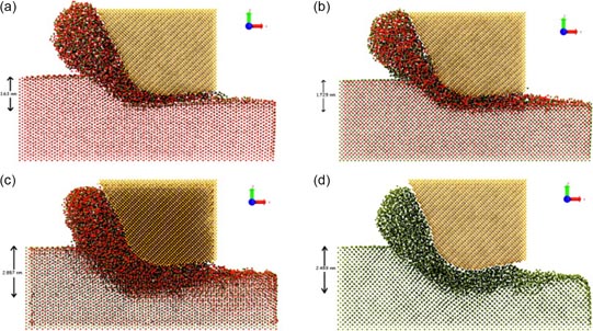
Figure 26. (a) Sub-surface crystal lattice deformed layer depth and chip morphology of 4H–SiC. (b) Sub-surface crystal lattice deformed layer depth and chip morphology of 3C–SiC. (c) Sub-surface crystal lattice deformed layer depth and chip morphology of 6H–SiC. (d) Sub-surface crystal lattice deformed layer depth and chip morphology of silicon. Reprinted with permission from [40], Copyright 2012 Elsevier.
Download figure:
Standard image High-resolution image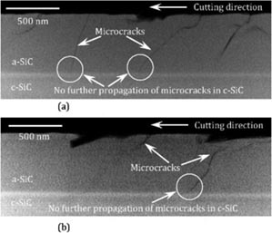
Figure 27. SEM results showing the control over the sub-surface damage [182]. (a) Close-up view of brittle-cut surface and (b) close-up view of ductile-cut surface.
Download figure:
Standard image High-resolution image5.2. Difference in machining of single crystal and polycrystalline SiC
Unlike in the machining of single crystal semiconductors, Yan et al [108] found that reaction bonded SiC (RB-SiC) does not undergo any phase transformation during its SPDT. They highlighted that the machined surface roughness on RB-SiC was significantly higher. Similarly, Patten et al observed a relatively high machined surface roughness while machining polycrystalline 3C–SiC [107]. Both these materials, i.e. 3C–SiC(CVD) and RB-SiC are polycrystalline materials (with appreciable differences in the g.b. and crystallographic orientations) while most of the observations stated earlier concerning the HPPT were valid only for single crystal materials. This raises a key question: How does chip formation change while machining a polycrystalline material compared to machining a single crystal material? To answer this question, Goel et al [36] developed an MD simulation model for the nanometric cutting of polycrystalline SiC workpiece and compared the mechanism of the deformation with that in a single crystal SiC (figure 28). They explained that in a single crystal SiC, the absence of grain boundaries causes tremendous lattice distortion which is responsible for the structural transformation of the cutting chips in single crystal SiC. Such phase transformations are, however, obstructed by the presence of grain boundaries during machining of the polycrystalline workpiece. In a polycrystalline SiC workpiece, the grains of SiC are oriented along different crystal orientations. Since grain orientation changes from one crystal to the other in polycrystalline SiC (except CVD SiC), the cutting tool experiences work material with different crystallographic orientations and directions of cutting. Thus, some of the grain boundaries cause individual grains to slide or cleave along the easy cutting directions. Consequently, the cutting chips in RB-SiC are not deformed by plastic deformation alone; rather, phase transformation at the grain boundaries and the slip/cleavage of the grains may both happen simultaneously. This is one of the most plausible reasons that silicon (used as sintering or bonding agents) at the g.b. underwent amorphization while no phase transformation of 6H–SiC grains was observed during experimental trials on RB-SiC [108]. An alternative explanation could be that slip at g.b. precedes or precludes HPPT (by relieving stress prior to the onset of HPPT).
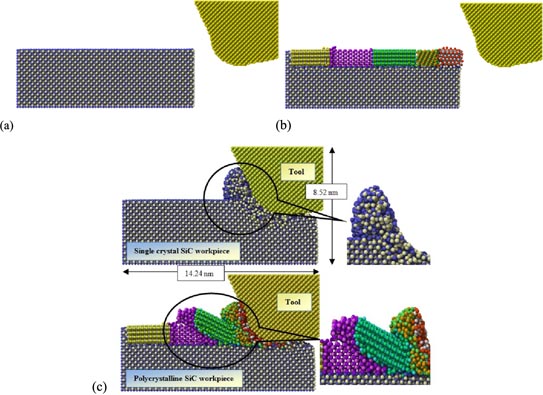
Figure 28. Snapshot from a simulation showing the response of the SiC workpiece during cutting. Reprinted with permission from [36], Copyright 2013 Elsevier. (a) Snapshot of a single crystal SiC before cutting, (b) snapshot of a polycrystalline SiC before cutting, (c) comparison of chip formation during machining of single crystal and polycrystalline SiC.
Download figure:
Standard image High-resolution imageIn polycrystalline brittle materials, grain refinement leads to the reduction of Young's modulus. While this scientific phenomenon is still being explored, some authors have attributed this to an increased volume fraction of grain boundaries, where atoms have weaker bonding than atoms in crystalline grains [183]. Furthermore, Szlufarska et al [184] reported that the crystalline SiC exhibits a crossover from a deformation regime in which grain boundaries hold crystalline grains like a glue to a regime that is dominated by discrete event plasticity. When the size of grains is in the nanometre regime, the deformation occurs due to the g.b. sliding and the material removal takes places by the dislodging of individual grains which is typical in a material like RB-SiC. Since the occurrence of cleavage in polycrystalline SiC occurs in a random manner depending on the ease of lowest cleavage energy offered by a particular grain, this explains the observation of slightly higher surface roughness in a polycrystalline material than that in a single crystal material. Goel et al [185] also calculated the average specific cutting energy for machining both types of SiC. Specific cutting energy is defined as a ratio of the work performed (cutting force × distance travelled) by the cutting tool to the volume of the removed material. The value obtained for polycrystalline SiC was found to be around 115 GPa which is relatively lower than the average specific cutting energy for single crystal SiC, i.e. 150 GPa [185]. This is because sliding along the easily cleavable direction in a non-uniform lattice will require less energy in comparison to that in cutting a continuous and uniform crystal lattice on a relatively harder direction of cut. This could explain why RB-SiC [108] and CVD–3C–SiC [107], despite having high surface roughness, were observed to be relatively more machinable than the single crystal SiC as observed in experiments.
6. Wear of diamond cutting tool
Figure 29 summarizes the problems of tool wear during the process of either conventional machining or diamond machining. Wear of diamond tools is an undesirable problem in SPDT not only because of the replacement cost but also because of its spurious effects on the attainable machined surface finish [185, 186]. In-process degradation of the diamond tool due to wear alters the tool–workpiece contact and hence the machining conditions can cause a sudden transition of material removal mechanism from ductile mode to brittle fracture in the cutting region with consequent deterioration of the machined surface finish. A good understanding of the tool wear mechanism is thus an essential step in identifying measures to suppress the tool wear.
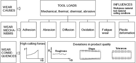
Figure 29. Implications of tool wear. Reprinted from [7] courtesy of J Patten.
Download figure:
Standard image High-resolution imageAn important explanation for periodic wear during diamond turning of RB-SiC has been provided by Zhang et al [180] who observed uniform and symmetrical wear marks on only one side of the diamond cutting tool. The wear marks were found to be fine microgrooves of uniform pitch and depth which they referred to as 'periodical groove wear'. Their careful inspection of the worn tools revealed that the width of the microgroove was equal to the feed/revolution signifying that the groove wear is an outcome of the replication of the tool feed on the machined surface. This mechanism not only prevails in RB-SiC but also on other nominal hard brittle materials as the region below the cutting region i.e. the plowing region, plastic deformation and more specifically the rubbing region, continue to undergo tremendous friction resistance with the workpiece. During this process, the feed marks of the tool are in resonance with the wear marks left on the cutting tool as highlighted in figure 30.

Figure 30. Schematic diagram of diamond turning. Reprinted with permission from [187], Copyright 2011 Springer. (a) Periodic wear marks observed during machining of RB-SiC, (b) new cutting tool and (c) worn cutting tool with flank wear.
Download figure:
Standard image High-resolution imageBy proposing a schematic diagram as shown in figure 31, it was explained further that the cutting edge of the tool continues to recede, and the flank wear region becomes predominant. This may be represented and understood as a kind of stagnation, as shown in figure 32, showing a point on the cutting edge radius where the tangential velocity of the workpiece becomes zero [188]. Notably, below the stagnation point, the material is compressed downwards in the wake of the tool. Above the stagnation point, the sheared material is more pronounced than the compressed material. Consequently, the sheared material is carried away as cutting chips.

Figure 31. Schematic of the groove wear. Reprinted with permission from [187], Copyright 2011 Springer.
Download figure:
Standard image High-resolution image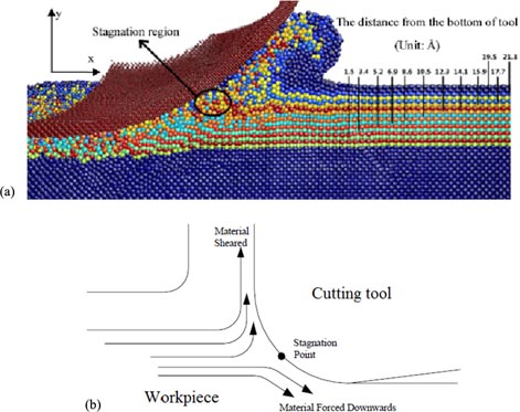
Figure 32. Stagnation point on the cutting tool during SPDT. (a) MD model (reprinted with permission from [189], Copyright 2012 Springer) and (b) schematic model.
Download figure:
Standard image High-resolution imageBased on this, it was explained that during nano-scale ductile cutting of brittle materials, the un-deformed chip thickness varies from zero at the centre of the tool tip to a maximum value at the top of the uncut shoulder. Thus, a 'zero-cutting zone' exists within which no chips are produced. In this zone, the tool acts more like a roller than a cutter and continuously slides on and burnishes the machined surface. Thus, flank wear causes a reduction in the clearance angle, and this gives rise to an increased friction resistance. This is the reason for a relatively high temperature at the tool flank compared to that at the rake face—a phenomenon that contrasts conventional machining where the tool rake face is at a higher temperature than that at the tool flank face. This happens because of the large amount of energy released from the cutting chips and the consequent heat dissipation into the tool rake face. In contrast, during SPDT, the effect of frictional heat between the tool flank face and the finished surface of the workpiece is more than that on the tool rake face. Subsequently, abrasion due to continuous friction contact with the flank face further enhances the wear rate, making the ratio of rake wear to flank wear minimal. While this explanation seems to provide a big picture of the wear process, the basic cause of the tool wear process was not clear. Using MD simulation, Goel et al [37, 40] investigated the mechanism of tool wear while machining single crystal SiC. They used the radial distribution function to explain the mechanism of tool wear as shown in figure 33.

Figure 33. Radial distribution function of the diamond tool during cutting of 3C–SiC. Reprinted with permission from [37], Copyright 2012 Elsevier.
Download figure:
Standard image High-resolution imageRelying on the accuracy of the potential energy function used, they explained that before cutting the radial distribution function, g(r), has a peak at 1.54 Å which is the known bond length of diamond while a few bonds on the surface (dangling bonds) result in a small peak at 1.42 Å. During machining, with the progressive advancement of the tool, this small peak continues to grow at the expense of the number of atoms with a bond length of 1.54 Å. This phenomenon was observed to be common for all the polytypes of SiC but with varying magnitude (figure 34). Thus, using g(r) sp3–sp2 transformation of the diamond tool was proposed to be the cause of tool wear during SPDT of all the major polytypes of SiC.

Figure 34. A comparison of the percentage of atoms from the diamond tool deformed during nanometric cutting of various polytypes of SiC (this is a major limitation of MD that the tool size is extremely small and tool wear is observed within a few nanometres of length of cut—a possible area where MD needs to advance further to study realistic machining processes). Reprinted with permission from [40], Copyright 2012 Elsevier.
Download figure:
Standard image High-resolution imageIn addition to quantifying the tool wear via g(r) or the measure of coordination number, it was also proposed that total displacement of each atom in the tool expressed as
 could be another useful measure to identify the progressive tool wear. The result obtained using such a method is shown in figure 35. Based on the outcome of the process discussed above, Goel et al [158] compared the process of diamond tool wear occurring during machining of single crystal SiC to that of polishing of a diamond with another diamond. They showed the sp3–sp2–sp disorder in the diamond tool in the form of figure 36 where silver colour atoms represent sp3; green colour represents sp2 while yellow colours represent sp arrangement. The regular arrangement of sp2 and sp bonds at the tool cutting edges represents termination of bonds (dangling bonds) on the surface and sides of the cutting tool. However, the sp3–sp2–sp bond transition around the tool nose appears as an initiation of the tool wear. Overall, research on the mechanism of wear of diamond cutting tools in general is still a growing area [97, 191–194] since it is limited by the robustness of the potential energy function to describe all the phases of carbon. Future research might be directed at identifying other phases of carbon, as well as developing more realistic potential energy functions, which may provide more accurate and detailed insights of wear processes.

Figure 35. Displacement vector of each atom in diamond tool after 10 nm of tool advance. Reprinted with permission from [37]. Copyright 2012 Elsevier.
Download figure:
Standard image High-resolution image
Figure 36. Wear of the diamond tool. (a) sp3–sp2 transition during SPDT of SiC [158]. (b) sp3–sp2 transition during polishing of diamond. Reprinted with permission from [190], Copyright 2011 Nature.
Download figure:
Standard image High-resolution image7. Future prospects
The review of current literature in previous sections provides several opportunities for new commercial, technological and scientific developments in the area of manufacturing of silicon carbide. In what follows, some recent developments are reviewed.
To explore the problem of heavy tool wear during machining of SiC, Goel et al [79] recently carried out a theoretical assessment of cutting silicon carbide using the so-called 'surface defect machining' (SDM) method [195–197] and compared the results with machining of SiC at an elevated temperature of 1200 K to emulate micro-laser assisted machining (μ-LAM) process [198] and normal machining at 300 K. In their simulation model (figure 37), surface defects were created on top of the SiC workpiece prior to the cutting operation which was inspired by their previous findings on hard steels. They generated surface defects in the form of a series of holes on the top surface of the workpiece prior to the actual machining operation by anticipating that the presence of such defects will reduce the bonding strength of the workpiece to provide the desired advantages of lower machining forces, reduction in overall temperature in the cutting zone, reduced machining stresses and increased chip flow velocity.

Figure 37. Snapshot from MD simulation for a 3C–SiC specimen with surface defects on top [80].
Download figure:
Standard image High-resolution imageFigure 38 shows a superimposed image and a comparison of the chip morphology from the MD simulation. On comparing nanometric cutting at 1200 K with conventional nanometric cutting at 300 K, there was an observed increase in the curliness of the cutting chips, plausibly due to increased plasticity of SiC at a high temperature of 1200 K without any appreciable change in the shear plane angle. This was however found to change significantly during machining with the SDM approach, wherein they observed an increase in the magnitude of the cut chip thickness and a corresponding reduction in the shear plane angle. They proposed that a decrease in the value of shear plane angle under the same machining parameters shows the dominance of tangential cutting forces over thrust forces which justify the enhanced cutting action of the tool.
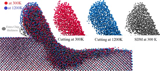
Figure 38. Chip morphology of 3C–SiC while cutting the workpiece under different machining conditions [80].
Download figure:
Standard image High-resolution imageThey further found that the extent of sub-surface crystal deformation lattice layer reduces while machining SiC using the proposed SDM method (figure 39) and also quantified the cut chip thickness to be higher during SDM. While the authors used MD simulation to assert these insights on the SDM of SiC, an experimental trial confirming this hypothesis is yet to be done and can be regarded as a promising research area. Another interesting research area is that of defect control in SiC wafers. Poor electrical reliability of SiC is still an area of concern. More research is needed to understand and overcome the material defect-induced problem in order to fully commercialize the SiC bipolar power devices. Some of these identified defects are shown in table 16.
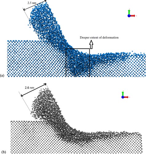
Figure 39. Comparison of sub-surface crystal lattice deformation of 3C–SiC [80]. (a) Cutting at 1200 K and (b) cutting at 300 K with SDM process.
Download figure:
Standard image High-resolution image
Table 16. Major types of crystal defects reported in SiC [31, 199].
| Crystal defect | Density in wafer (cm−2) | Density in epilayer (cm−2) | Comments |
|---|---|---|---|
| Hollow-core axial screw dislocation | 10–100 | 10–100 | Causes severe reduction in power device breakdown voltage |
| Closed-core axial screw dislocation | 103–104 | 103–104 | Causes severe reduction in device breakdown voltage and increase in leakage current |
| Basal plane dislocation | 104 | 102–103 | Causes bipolar power device degradation and reduction in carrier lifetime |
| Threading-edge dislocation | 102–103 | 104 | Impact not well identified yet |
| Stacking faults | 10–104 | 10–104 | Faults known to degrade bipolar power devices, reduce carried lifetime |
| Carrot defects | N/A | 1–10 | Severe reduction in power device breakdown voltage and increase in off-state leakage |
| Low-angle grain boundaries | 102–103 | 102–103 | Impact not well identified yet |
Overall, the emergence of various ultra-precision machining advancements such as diamond machining and the continually challenging demands of machining difficult-to-machine materials such as SiC are leading to much improved understanding of various machining processes. In particular, the advantage of modelling needs to come into practice to lead to the proof-of-concept experimental trials [200]. The HPPT, in particularly, at elevated temperatures, e.g., micro-LAM, need to be accurately modelled with more robust potential energy functions. In the upcoming years, MD simulation is thus expected to contribute significantly to the field of contact loading [201–203] while improving the knowledge on diamond machining of SiC.
8. Concluding remarks
The mechanism of nanometric cutting of silicon carbide is influenced by a number of variables such as machine tool performance, machining conditions, the material's properties, and cutting tool performance (material microstructure and physical geometry of the contact), and all of them cannot be monitored online through experimental examination. These could be suitably studied using an advanced simulation based approach such as molecular dynamics (MD) simulation. This review detailed how MD simulations have made and continues to make significant contributions to the understanding of several aspects of diamond machining of silicon carbide. The world of MD simulations is dependent on present day computers and the accuracy and reliability of potential energy functions [204]. This presents a limitation: real-world scale simulation models are yet to be developed. The simulated length and timescales are far shorter than the experimental ones. Also, simulations of nanometric cutting are typically done in the speed range of a few hundreds of m/sec against the experimental speed of typically about 1 m s−1 [186]. Consequently, MD simulations suffer from the spurious effects of high cutting speeds and the accuracy of the simulation results has yet to be fully explored. The development of user-friendly software could help facilitate molecular dynamics as an integral part of computer-aided design and manufacturing to tackle a range of machining problems from all perspectives, including materials science (phase of the material formed due to the sub-surface deformation layer), electronics and optics (properties of the finished machined surface due to the metallurgical transformation in comparison to the bulk material), and mechanical engineering (extent of residual stresses in the machined component) [205]. Overall, this review provided key information concerning diamond machining of silicon carbide, which is summarized as follows:
- 1.The ductile response of SiC is a hotly debated issue and a number of mechanisms regarding ductility in SiC have been proposed. Overall it can be asserted that crystal anisotropy of SiC certainly influences the mechanism of deformation of SiC and is thus vital in overall understanding of the plastic deformation in SiC.
- 2.MD simulations have revealed that 3C–SiC exhibits a strong degree of crystal anisotropy of upto 44% signifying certain favourable combinations of crystallographic orientations favouring ease of deformation (it may be noted that only simulation based studies are done on cutting of single crystal 3C–SiC due to unavailability of large size specimen of this material to date). An overall analysis of the machining stresses, temperature in the machining zone and cutting forces obtained from MD simulations suggested that the amenability of single crystal 3C–SiC being cut in particular crystal setups can be tabulated as follows:
Crystallographic planes Least amenable cutting directions More amenable cutting directions Cube (0 0 1) 〈−1 1 0〉 〈1 0 0〉 Dodecahedron (1 1 0) 〈−1 1 −2〉 〈0 0 1〉 Octahedron (1 1 1) 〈−2 1 1〉 〈−1 1 0〉 - 3.Despite being a compound of silicon and carbon, the mechanism of deformation of 3C–SiC is closer to diamond than silicon. For example, the material removal on (1 1 0) 〈0 0 1〉 crystal setup in single crystal 3C–SiC (soft scratching direction of both 3C–SiC and diamond) was dominated by structural transformation whereas cleavage was observed to be a dominant mechanism of material removal on the (1 1 1) crystal orientation during nanometric cutting of 3C–SiC.
- 4.An important aspect associated with machining SiC is the strong polymorphism exhibited by SiC across its polytypes, among which 3C–SiC, 4H–SiC and 6H–SiC have been more rigorously explored for commercial applications. A significant variation in the indicated quality of the machined surfaces and the sub-surface crystal lattice deformed layer depths was observed in various polytypes of single crystal SiC simulation under the same machining parameters using MD simulation. Simulations showed that single crystal 4H–SiC would produce the best sub-surface integrity followed by single crystal 3C–SiC and single crystal 6H–SiC.
- 5.Research shows that both chemically vapour deposited (CVD) SiC and reaction bonded (RB-SiC) are easier to machine than single crystal SiC. This is because of the fact that the cutting chips in polycrystalline material like RB-SiC are deformed both by a combination of the phase transformation at the grain boundaries and the slip of the grains in tandem.
- 6.MD simulations have shown that the diamond cutting tool would undergo sp3–sp2 disorder due to mechanical abrasion against all the polytypes of SiC which is the phenomenological reason of tool wear during machining of SiC.
Acknowledgments
The author greatly acknowledges the funding support from the International Research Fellowship account of Queen's University, Belfast in motivating the need for this review. The author would like to thank in particular Professor John Patten (Western Michigan University, USA) for laying a sound foundation in this area. Author also extends sincere thanks to Dr Anupam Agrawal (UIUC, USA), Professor Xichun Luo (University of Strathclyde, UK), Professor Jiwang Yan (Keio University, Japan) and Dr Alexander Stukowski (Darmstadt University of Technology, Germany) for their support.
Footnotes
- 1
Readers are referred to the web based version of this article to interpret the correct colour legends.
- 2
Personal communication with Prof. John Patten at Western Michigan University, USA.