Abstract
We describe the layout and unique features of the focal plane system for MIRI. We begin with the detector array and its readout integrated circuit (combining the amplifier unit cells and the multiplexer), the electronics, and the steps by which the data collection is controlled and the output signals are digitized and delivered to the JWST spacecraft electronics system. We then discuss the operation of this MIRI data system, including detector readout patterns, operation of subarrays, and data formats. Finally, we summarize the performance of the system, including remaining anomalies that need to be corrected in the data pipeline.
Export citation and abstract BibTeX RIS
1. Detector System Overview
The science potential of the James Webb Space Telescope (JWST) is derived from the rapid advances over the past three decades in performance and size of infrared arrays. Some of the applications are discussed in Gardner et al. (2006). The greatest gains with JWST will be in the deep thermal infrared, where the high backgrounds on the ground have compromised the infrared array performance and previous cooled telescopes in space have had small apertures and limited angular resolution; see Rieke et al. (2014a, hereafter Paper I).
To implement fully the deep thermal infrared capabilities of the JWST, the Mid-Infrared Instrument (MIRI) uses three arsenic-doped impurity band conduction detector arrays, each of 1024 × 1024 pixel format with 25 μm pixel pitch. The performance expected is described in Glasse et al. (2014, hereafter Paper IX). These detectors have heritage to the Si:As devices used in all three Spitzer instruments, but particularly to the arrays in the Infrared Array Camera (IRAC) (Fazio et al. 2004; Hora et al. 2004). Like the IRAC arrays, the MIRI devices were manufactured by Raytheon Vision Systems (RVS) in Goleta, California. Both array types use a customized cryogenic readout process to provide stable performance at low temperature, and their detectors are generally similar in terms of doping levels, layer thicknesses, and pixel pitch.
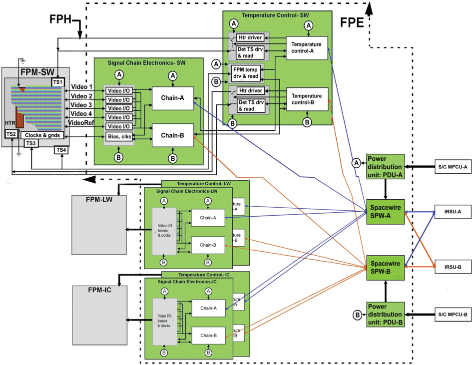
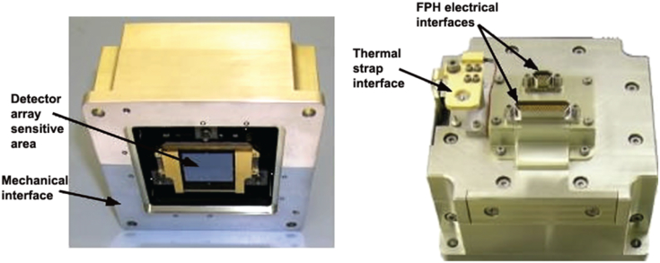
The MIRI detector system, or more formally the focal plane system (FPS), is shown as a block diagram in Figure 1. It is composed of three entities: the focal plane modules (FPMs), the focal plane electronics (FPE), and the focal plane harness (FPH). A FPM houses a detector array and locates it at the relevant focal plane provided by the optical assembly (see Figs. 2 and 3). There are three FPMs: one for the imager, and one each for the shortwave and longwave channels in the medium-resolution spectrometer (MRS). The 4 m long FPH carries all electrical signals between the FPMs and the FPE. The FPE consists of the control and readout electronics for the detectors and also monitors and controls the temperature of each FPM to within 10 mK. Each of the FPMs is driven by separate signal chain electronics and temperature control slices, with internal block redundancy (sides A and B). Our discussion of this system begins with FPMs (§ 2) and FPE (§ 3), followed by a description of the operation of the full FPS (§ 4) and a description of the performance of the system (§ 5). Future work is previewed in § 6.
Fig. 1. Block diagram for the MIRI focal plane system. The uppermost of three identical input electronics trains is enlarged for clarity.
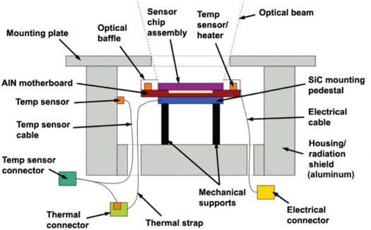
Fig. 2. Schematic diagram for the MIRI focal plane modules.
Fig. 3. Front and back views of a FPM. The aluminum housing is roughly 11 cm across; the detector array sensitive area is approximately 26 mm × 26 mm square.
2. Focal Plane Module
2.1. FPM Design
Each FPM (see Sukhatme et al. 2008) has a detector assembly (DA) and its housing (Fig. 2). The DA includes the detector sensor chip assembly (SCA), heaters and temperature sensors, a fan-out board, a mechanical pedestal, an electrical ribbon cable, and connectors for the signals to and from the SCA and for the temperature sensors (see § 2.3). The FPM housing provides opto-mechanical alignment, structural support, and thermal isolation for the DA (Fig. 3). The housing has two auxiliary temperature sensors to help monitor the thermal environment, and it is 20 mm thick, so it also provides a major portion of the radiation shielding for the detectors.
The DA mounting structure was designed to meet both the detector thermal isolation requirements and provide the mechanical integrity to withstand launch loads and the thermal expansion mismatch between the DA and the FPM housing. The detector assemblies are supported within their housing by a thermally isolating rod structure. This supporting structure keeps the alignment of the sensitive surface of the detector array to within a 50 μm radius of the nominal detector position in x - y, and within ± 20 μm in z/tip-tilt through the launch environment and from room temperature down to an operating temperature of 6.7 K or less.
For stray light reduction, serpentine, thermally insulating ports are provided to pass the electrical cable and thermal strap through the housing backplate. The cable is then attached to a thin aluminum bulkhead that provides mechanical support for the connectors. The thermal strap is supported by an insulating post and also connected to a thermal interface plate. This plate is where the external heat strap is attached to provide cooling for the SCA.
2.2. Sensor Chip Assemblies
To manufacture the sensor chip assemblies for MIRI, the detector layers were grown to MIRI-specific requirements, diced, and patterned with indium bumps, then bonded via matching indium bumps to the cryo-CMOS silicon readouts. The resulting hybridized arrays are antireflection (AR) coated with one of two possible single layer AR coatings, one optimized for 6 μm and the other for 16 μm. Contrary to usual practice, to minimize interpixel capacitance the hybridized arrays were not backfilled with epoxy; subsequent qualification testing proved the epoxy was unnecessary for mechanical support purposes. More information about the detectors is provided in Love et al. (2005) and Rieke et al. (2014b, hereafter Paper VII).
The readouts for these detectors are based on the cryogenic silicon circuit process developed for IRAC and the far infrared detectors of MIPS on Spitzer and described in an early form by Lum et al. (1993). In this approach, the circuitry is put on a thin surface layer of the silicon wafer; this layer is grown on a degenerately-doped silicon substrate. This design brings the ground plane through the substrate and close to the circuit even at very low temperatures, improving the low-temperature electronic stability.
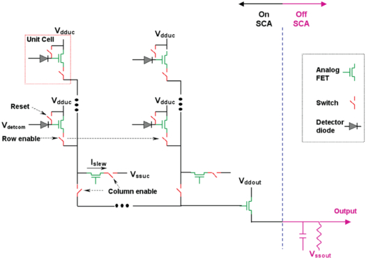
The readout circuit is shown schematically in Figure 4, including four unit cells (each with an analog source follower FET and a reset switch FET), the row and column select transistors, and the output amplifier. An initial charge is placed on the detector node capacitance through the Vdduc supply when the reset switch is closed to establish the detector bias voltage. The detector bias voltage is set by the difference between Vdetcom (applied to the transparent buried contact—see Paper VII) and Vdduc (applied to the indium bump contact). There is an additional ∼0.2 V placed on the node from clocking feedthrough so that the final applied bias voltage is Vdduc - Vdetcom + 0.2 V. After the switch is opened, photocurrent drains the charge in proportion to the optical signal. The node voltage is buffered by a source follower within the unit cell, then passed to the output source follower/line driver through the row and column select switches.
Fig. 4. Electrical schematic for the MIRI readout integrated circuit. Four representative unit cells are included along with the row and column multiplexing switching FETs and the output amplifier. The detectors themselves are indicated as diodes because of their asymmetric electrical characteristics.
The completed hybridized SCA is mounted on an aluminum nitride motherboard, a material selected because its thermal contraction upon cooling approximately matches that of the silicon detector array. The interface structure between the array and motherboard is designed to minimize the residual stresses on the array.
2.3. Detector Assembly
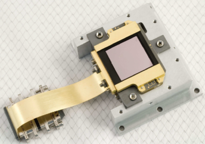
A picture of one of the MIRI detector assemblies is shown in Figure 5. The SCA is visible as a gray square in the center. The multilayer aluminum nitride (AlN) fan-out board is mostly covered by the gold-coated light shield, but may be glimpsed at the lower right edge of the shield. This, in turn, is mounted on a silicon carbide (SiC) mounting pedestal which has six cylindrical bushings (three visible) that serve as the mechanical interface to the FPM housing.
Fig. 5. Photograph of a MIRI Detector Assembly. The 26 mm × 26 mm detector sensitive surface is visible as the square in the center. Other components such as the temperature sensors, the filter resistors and capacitors, etc., are located on the fan-out board under the gold-coated portions of the light shield. The plain aluminum structure is a shipping bracket and not part of the DA.
A cable assembly that is electrically attached to the fan-out board but mechanically supported by the pedestal conveys electrical signals to and from the SCA. Temperature sensors, heaters, and some R–C filters are mounted on the motherboard, but are covered by the light shield. The electrical interface is a 51-pin micro-D MDM connector. The thermal interface is through a tab on the bottom of the SiC pedestal to which a copper thermal strap is attached. The materials for the DA (AlN and SiC) were chosen to have matching thermal expansion characteristics.
3. Focal Plane Electronics
3.1. FPE Design
Located in the room-temperature thermal zone behind the telescope (specifically, in the ISIM electronics compartment (IEC; see Greenhouse et al. [2011] for an overview of the ISIM and IEC)), the FPE contains all of the control and readout electronics for the three detectors (Fig. 1). Power is received from the JWST Integrated Science Instrument Module (ISIM) and is converted to the requisite DC voltages needed within the FPE by a power-distribution unit (PDU) board (to the right in the figure). There are primary and redundant PDUs within the FPE. Commands are received via a SpaceWire communications interface board from the ISIM instrument control and data handling (ICDH) system and are interpreted by the FPE SpaceWire interface cards (SPW, primary and redundant, also to the right). Valid commands are then transmitted to the signal chain electronics (SCE) boards (one per detector, with primary and redundant sides on each board—to the left center, with the short wave [SW] detector channel enlarged for clarity), where the clock and bias signals are generated (video I/O, one signal chain for each of the four array outputs and a fifth for the reference output) and sent down the harnesses to the detectors (extreme left, SW channel enlarged for clarity).
As directed by the clock signals, analog signal voltages from the detector are multiplexed and sent serially through the harnesses to be collected by the SCE video I/O boards, where they are amplified and digitized. The digital signals are packetized in the SPW boards (to the right) and then delivered to the ISIM Remote Services Unit (IRSU, extreme right) where they are stored for later transmission to the ground. The SCE boards also collect telemetry reporting the detector control voltages and the board supply voltages to monitor the health of the system. These are also sent back through the SPW boards, though in separately identified packets.
The detector temperature control is provided by temperature control electronics (TCE) boards, again one per detector (center of the figure, enlarged for the SW channel). The control is a relatively standard proportional-integral-derivative (PID) feedback algorithm, although the differential term is hard-coded to zero. Due to a flaw in the embedded heaters that are located immediately under the detectors in the FPMs, we use the temperature sensors located at opposite corners of the SCAs also as heaters since they are simple resistive elements (though highly temperature sensitive!). The TCE board drives power through the temperature sensor for 88% of a 100 ms drive cycle; for the other 12%, the power is reduced to sensing levels and the temperature is measured. When self-heating in the sensor is taken into account, this provides a robust thermal control circuit, with drifts of less than 1 mK (as monitored with the redundant sensor using ground support electronics).8
3.2. Readout Process
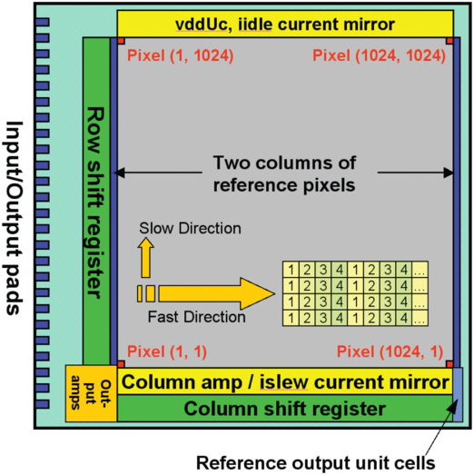
A representation of the full MIRI readout is shown in Figure 6. The SCA has a total of 1024 × 1024 active pixels. There are four additional "reference pixels" at the beginning of each row and four at the end that are not connected to detectors, but in all other ways are treated as light-sensitive pixels. All these pixels (including the reference pixels) are read out through four interleaved data outputs; each output presents 258 × 1024 pixels to the signal chain electronics for processing. The outputs are read simultaneously, so at a sampling rate of 10 μs per pixel, it takes slightly less than 3 s to read out the full array. Clock patterns control the row and column shift registers to address the individual pixels for either destructive or nondestructive reading. Note that all readout patterns start closest to the output amplifiers (lower left-hand corner) and this fact has been used to determine a preferred orientation of the SCAs with respect to the various instrument focal planes. There is an additional, fifth "reference output" that is a group of blind pixels that are sampled continuously (and simultaneously with the four data outputs) and that can be used for various engineering and data quality-monitoring purposes. Since this signal also appears as a 258 × 1024 pixel data stream that is interleaved with the four data channels, the SCA effectively presents a 1290 × 1024 pixel "image" to the outside world.
Fig. 6. Schematic of the readout multiplexer. The square area (gray) marked by the pixel corners corresponds to the light sensitive pixel region. The two narrow columns (blue) on the left and right of the light sensitive region identify the two sets of four columns of reference pixel locations. Row and column shift registers (dark green) border the pixels on the left and bottom and address pixel locations. The arrows and repeating 1234 numbers show schematically the pattern by which the SCA is read out. The bond pads for the FPE signals are located on the left side of the array.
The pixel coordinate system starts with "1," not "0." Zero has a special value to the readout shift registers, and so the first physical pixel (actually the left-edge reference pixel) starts at column 1. The first light sensitive pixel starts at column 5 and ends with column 1028; the last right-edge reference pixel is column 1032. There are no reference pixels along the top or bottom rows, so the rows are all active and range from 1 to 1024.
4. FPS Operation
4.1. Electronics Upgrade
The signal chain electronics (SCE) boards used for the flight instrument testing have a flaw that produced occasional corrupted science data frames. These boards have been redesigned to eliminate this problem, but with the requirement that they be pin-compatible with the original boards and therefore that they preserve the basic operational characteristics of the system. Nonetheless, the new boards include a number of additional improvements. The boards are being switched at the end of 2014, and the final flight data system for MIRI will be validated and calibrated during the third cryo-vacuum test of the ISIM in the second half of 2015. We describe the operation of this system below.
4.2. Individual Frames
The FPS is controlled by commands received from the ICDH via the MIRI flight software; it acts on them and returns science and telemetry data. All three detectors are operated independently via the three SCE boards, but in a similar fashion (i.e., there are no commands unique to individual arrays). Observers will define their exposures from a palette of readout patterns that have been predefined to support the full capability of MIRI. The readout patterns for MIRI fall within the framework of the general MULTIACCUM readout patterns adopted by the JWST mission so that all instruments will have similar exposure interfaces.9
The general scheme for reading out the SCA, referring to Figure 6, starts with addressing row 1 and then reads left-to-right through all 1032 columns (four at a time) before proceeding onto row 2, etc., until row 1024 is completed. Thus, the "fast" direction of the readout is across each row and the "slow" direction is up the columns. The four outputs present four pixels simultaneously to the electronics in a [1234] pixel pattern; this block of four pixels repeats 258 times to complete an entire row of 1032 pixels. Recall that the first four and last four pixels of each row are reference pixels. The fourth readout line, e.g., is responsible for every fourth column of data in the final image and will produce a "jailbar" pattern in the raw frames if its offset differs substantially from the other outputs.
The pixels are reset by row pairs (i.e., 2 rows, 2064 pixels, at a time). For example, row 1 will be read, then row 2 will be read, then they will be reset together, then row 3 will be read, etc. The column and row shift registers must be clocked through the entire SCA before returning to a given odd-numbered row. This approach enables a final read immediately before resetting the SCA, and thus captures the longest possible integration time. The disadvantage of this approach is that one cannot read the values immediately after reset, and thus the reset level (as in a traditional correlated double sample) cannot be obtained.
4.3. FASTMode and SLOWMode
The electronics have the ability to sample an individual pixel multiple times before moving on to the next pixel (sometimes referred to as "dwell"). In "FASTMode," MIRI samples a pixel once during a single clock cycle spent on that pixel. However, in "SLOWMode," ten samples of a pixel are obtained and a subset of them can be averaged (e.g., four or eight) to output a single result from the FPE to the IRSU, within an overall cadence of ∼30 s. This approach can reduce MUX glow, e.g., since it is no longer necessary to read the pixel every ∼3 s as in FASTmode. However, SLOWMode, because of the 30-s readout time, is most appropriate for faint source and/or low background work.
4.4. Clocking Patterns
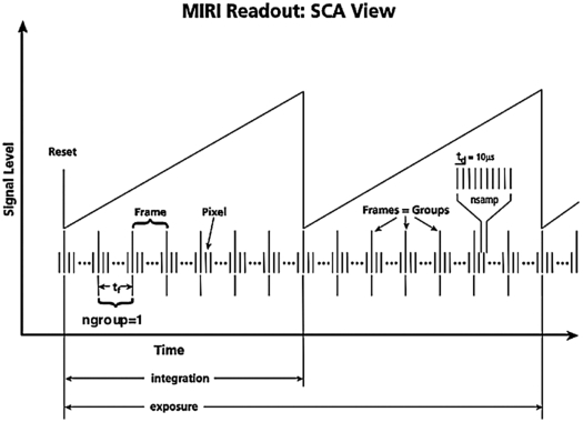
A schematic MIRI readout timing pattern is shown in Figure 7. In describing it, we adopt the detector lexicon of the JWST Mission Operations Concept Document for reference.
Fig. 7. Clocking patterns to read out the MIRI arrays. A representative integration ramp is included to help illustrate the definitions of key terms.
The underlying approach is always used to address the SCA at a constant rate (whether exposing or not) to maintain the stability of the SCA properties, in particular, the SCA temperature as well as slowly varying electrical properties. The pixels of the SCAs will be continuously addressed at time intervals of 10 μs, which is the time between pixel samples, td, and which is set by the FPE master 100 kHz clock. The general MIRI timing pattern is defined by only three of the MULTIACCUM parameters: (1) nsample, the number of samples per pixel (for MIRI, this will either be 1 for FASTMode, or 10 for SLOWMode), (2) ngroups, the number of groups during an integration, where a group is the product of cycling through all the pixels, and (3) nint, the number of integrations during an exposure, where integration is defined as the time between resets. By definition, for MIRI, there is exactly one frame per group, so that "frames" and "groups" could be used interchangeably. The value of nsample (the READMODE parameter given above) determines the time between frames, t1. The value of ngroup determines the integration time, tint, as follows: tint = ngroup × t1. For example, ten frames of FASTMode yield a tint = 10 × 2.775 = 27.75 s or ∼30 s. Note that with MIRI SCAs, the delta time between groups, t2, is zero. An exposure consists of one or more identical integrations. The value for nint determines the exposure time as follows: texp = nint × tint. For example, if we expose for five integrations with a tint = 27.75 s, then texp = 138.75 s and during this exposure time there were five resets of the array. There is no "dead time" between frames or integrations, so the wall-clock time for an exposure is an integral multiple of the single frame time. MIRI receives commands only at an exposure boundary, so an exposure with its various parameters is the lowest level of external commandability of MIRI.
One advantage of the MULTIACCUM readout mode is that cosmic rays can be rejected using ground-based software that processes pixel samples taken before and after a cosmic ray hit. MIRI can take maximum advantage of such software because MIRI plans to download all its data to the ground for processing, except in some high-data-volume cases. Rauscher et al. (2007) studied the effects of cosmic rays on the imaging exposure times on the JWST near-IR cameras, and these results are applicable to MIRI. For an anticipated cosmic ray flux of 5 protons cm-2 s-1, they expect that 20% of the pixels will be affected in a 1000-s exposure. However, the data pipeline is planned to identify cosmic ray hits within integration ramps and recover the data prior to and after them, to improve efficiency. Regan & Stockman (2001) discuss how MULTIACCUM type readout facilitates integration times longer than 1000 s. The advantages of this approach have been demonstrated on-orbit by the NICMOS instrument on the Hubble Space Telescope (HST) and the Spitzer/MIPS germanium detectors. We have demonstrated these approaches for MIRI by testing various slope fitting algorithms described by Fixsen et al. (2000) and Offenberg et al. (2001) on data taken with flight and flight-like MIRI sensors.
Thus, the integration time is determined not by how long it takes for a specified fraction of pixels to be hit by cosmic rays; rather, it is set by how long it takes for other noise sources to dominate. For broadband imaging, the optimum integration time will typically be the time required to become background limited. For MRS spectroscopy, the integration time should be influenced by the time required to become dominated by shot noise on detector dark current. Nonetheless, there will be residual noise from cosmic rays that do not free many electrons, as well as an accumulated bias shift from multiple hits. It may be desirable to reset the detectors periodically to restore the bias voltage on them. Also, low frequency instability of the detector readout and electronics may be the dominant noise in long integrations.
4.5. Data Format Including the Reference Output Line
As described above, the MIRI SCAs have two types of reference signals to assist with noise reduction: the left- and right-edge reference pixels, and the reference output. The reference output is sampled simultaneously with the four science data outputs, so that a full output frame is effectively 1290 × 1024 pixels. In addition to science frames (to be sent to the ground), the data are used by the ICDH scripting engine to provide target acquisition and centering information. To have a valid image, the scripts must skip every fifth pixel (the reference output) as they ingest data.
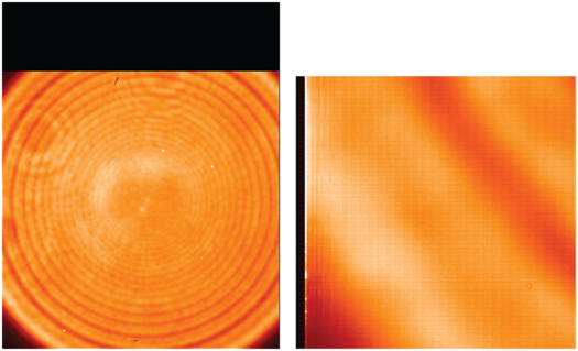
The signal level in the reference output line may be substantially different from the data output lines (especially in the case of high background images), which will affect the compressibility of the data. To improve this compressibility, the ICDH system rearranges the data stream coming from the MIRI FPE so that all reference output pixels will be placed at the end (top) of each frame as shown in Figure 8, not in every fifth column. This is the format that will be sent to the ground and will appear in the "Level 1" (raw) FITS files.
Fig. 8. Real data after it has been rearranged with the reference output data at the top. The reference pixels are along the side of the array as seen in the magnification at right. The bullseye illumination is an artifact of the light source. These data were obtained at JPL using flight-clone electronics but without the MIRI optical module.
4.6. Subarrays
The MIRI SCAs have the ability to read out partial frames through the manipulation of the clocking patterns. This allows a reduction in the frame time, and thus will allow integration times of substantially less than 3 s. For all subarrays, the subarray portion (the region-of-interest, ROI) is read out and stored while the remaining rows of the array are continually reset.
The subarray coordinates cannot be randomly accessed; one must step the row and column shift registers from the origin (1,1) to the starting subarray corner before proceeding. So at the beginning of the frame read, the first two rows of the full array are accessed briefly and reset, then the second pair, etc., until the ROI is reached. For more efficient subarray operation, a "burst mode" clocks through the left-hand columns at 5 times the normal speed. In the first row of the ROI, the pixels on the left that are not part of the ROI are clocked through (and not digitized), after which the pixels that are part of the ROI are read. The pixels to the right of the ROI are ignored by resetting the column shift register to 0 (recall the special shift register definition) immediately after the last ROI pixel. This pattern is repeated through all the rows contained within the ROI. The rows after the ROI are stepped through quickly and reset as were the rows before the ROI.
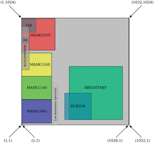
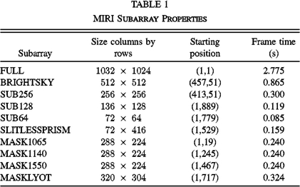
There are consequences to having to clock through the pixels on the left side of the ROI. Suppose one wishes to observe with the SUB256 (256 × 256 pixel) subarray that starts at pixel (413,51). The clocks quickly sweep through the first 50 rows (70 μs per row or about 3.5 ms total), but when one gets to row 51, 412, columns to the left of the ROI must be skipped. If we could not quickly burst through them, 103 cycles would be needed to get to the ROI (recall we access four columns at a time), then 64 more cycles are needed to read the pixels within the ROI itself (plus a few cycles of overhead) for a total of 1.77 ms per row, or 453 ms for all the rows containing the ROI. However, since we can choose to burst through the 412 columns at 5 times the normal rate, it takes only 21 periods of 10 μs (or 103/5, rounded up) to get to the ROI, for a total of 0.96 ms per row or 246 ms for the area. The 718 rows after the ROI are also clocked at 70 μs-1 per row for an additional 50 ms. The total frame time is the sum of these three totals, 300 ms for the case where we use burst clocking versus 507 ms where we do not. This compares to the 243 ms that are needed to read a same sized subarray that starts in Column 1. Therefore, subarrays become slower the farther they are from the left hand edge of the array, though this is compensated somewhat by the use of burst clocking. This fact drove the orientation of the imager array, since it is advantageous to have the fastest subarrays located within the coronagraph.
As a result of the constraints, the arrangement of subarrays and the resulting minimum integration times (and maximum fluxes) are complex. A summary is provided in Table 1, with more discussion in Papers III and IX. Figure 9 identifies the proposed subarrays and their applications. To ensure consistent calibration of subarray modes, only a few subarrays will be supported and the user will have to select from these predefined versions. There are nine in total: (1) one for each of the four coronagraphic areas; (2) one for high backgrounds; (3) three for bright objects; and (4) one for slitless low resolution spectrometer (LRS). Subarray modes are only useful and provided for the MIRI imaging SCA, not the MRS.
Fig. 9. Positions of subarrays in the imager field-of-view.
|
There are multiple considerations that led to the specific arrangement in Figure 9. The total number of pixels contained within a subarray must be a multiple of 64, including the reference output values, to fit well into the ICDH architecture. The coronagraph subarray locations and sizes are determined in part by the final focal plane mask design; however, the actual size of the coronagraphic subarray may be larger than its field-of-view to accommodate the multiple of 64 requirement on the subarray size. The coronagraph fields of view may be used for both target acquisition procedures and science data. The size for the high background subarray (512 × 512 pixels) is determined by the dynamic range needed to image faint sources in the background glow of the Orion Nebula region. The sizes for bright object subarrays are driven by the saturation limits needed to observe known radial velocity planet host stars, but limited by the fact that going below a 72 × 64 subarray does not yield a significantly faster pixel clocking speed because of the overheads discussed above. The size of the slitless prism subarray is determined by the number of pixels needed to cover the 5–12 μm LRS spectrum in the dispersion direction and to provide adequate sky observations for background subtraction in the spatial direction.
5. Performance
5.1. Electro-optical properties
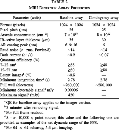
The basic performance of the MIRI detector arrays is described by Ressler et al. (2008) and summarized in Table 2. That paper describes the measurements of quantum efficiency, response versus detector bias voltage, read noise, well depth, and a number of other parameters that are not necessary to update. We describe below areas where significant changes in methodology have occurred since publication of that paper.
|
As described in Table 2 and in Paper VII, there are two slightly different detector architectures in the MIRI arrays, termed the baseline and the contingency designs. The contingency array (used in the short wavelength arm of the MRS) trades a lower absorption efficiency (due to lower doping and a thinner IR-active layer) for reduced dark current. The baseline array type is used in both the imager and the long wavelength arm of the MRS, but with the 6 μm AR coating for the former and the 16 μm one for the latter.
5.1.1. Pixel Gain
The pixel gain, defined as the digital numbers out of the electronics per electron placed on the integrating node of an array amplifier, is a critical parameter for interpretation of many aspects of array and instrument behavior. We have measured the gain by injecting a test voltage into Vdduc and tracking Vdetcom with that variation (to keep the detector bias constant at 2.0 V). Please refer to Figure 4 for the roles of these voltages. By monitoring the FET output as a function of Vdetcom, we find a net system gain of 38,300 DN V-1, where V is the voltage into the integrating node. To convert this measurement to a pixel gain requires the capacitance of the integrating node. The value for the input to the MIRI multiplexer has been measured to be 28.5 fF (McMurtry et al. 2005), to which we need to add contributions from a detector pixel (1.1 fF from basic physics) and from the bump bond interconnects between the detectors and their amplifiers (about 4 fF, e.g., Moore [2005]). For the resulting estimate of 33.6 fF, the gain is ∼5.5 electrons DN-1; i.e., a signal of 5.5 electrons from a detector results in one DN change in the FPE output.
5.1.2. Dark Current
Dark currents in the flight detector arrays were measured as part of the flight model instrument test campaign. The contamination control cover (CCC; see Paper II) was closed to make the instrument interior as dark as possible (although as always one can measure only upper limits to the true dark current, given the possibility of photon leaks). In processing the data, the first and last frames of an integration ramp were rejected, to circumvent the effects of the reset anomaly and last-frame effect (see below). Dark currents were then determined by the slopes of the integration ramps over a 100 × 100 pixel region selected to avoid bad pixels. The slope calculations included all exposures in a test run; the effects of settling of the detector output artificially elevate the apparent dark current, again making the results upper limits.
5.1.3. Imaging Properties
The response of the arrays is uniform, with pixel-to-pixel variations of no more than 3% rms. The best arrays have a small proportion of inoperative pixels (either hot or dead), of order 0.1%.
The imaging properties of MIRI were measured multiple times during the buildup of the instrument modules and then in the test of the flight model prior to delivery, and finally in the Integrated Science Instrument Module (ISIM) test post delivery. The most precise of these measurements in terms of the array performance were conducted at CEA with just the imager, and illuminated by a source outside the cryostat with extensive filtering to control the background emission (e.g., Ronayette et al. 2010). The point-spread function (PSF) measurements utilized a microstepping strategy so that many positions of the source were recorded on centers smaller than the pixel pitch of the MIRI array. These measurements were then converted to a high-resolution PSF image. The images at the longer wavelengths are as expected (Paper VII), showing excellent imaging properties from the array with only a low level of crosstalk. We have measured the pixel-to-pixel crosstalk in a number of ways (Finger et al. 2005; Regan & Bergeron 2012; Rieke & Morrison 2012), including autocorrelation, analysis of cosmic ray hits, and of hot pixels. All measurements indicate a level close to 3% for the crosstalk to the four adjacent pixels around one receiving signal. A plausible cause of this behavior is interpixel capacitance, although there may be secondary contributions from electron diffusion and optical effects (Rieke & Morrison 2012). In addition, at 5.6 μm there is an additional cross-like imaging artifact, discussed in more detail in Paper VII.
5.2. Nonideal Behavior
In common with most infrared arrays, the MIRI arrays show a variety of nonideal behaviors, the most important of which are described below. With the exception of the last-frame effect, previous generations of Si:As IBC detector arrays show all of the effects seen in the MIRI ones. The goal of the ongoing pipeline development is largely to mitigate these effects, making use both of experience with previous similar detector arrays and through a test campaign with similar arrays and electronics, with analysis of the results by the MIRI pipeline development team. The primary areas of interest are listed below.
5.2.1. Reset Anomaly
With the MIRI arrays, the first few samples starting an integration after a reset do not fall on the expected linear accumulation of signal. This behavior is seen in virtually all types of infrared arrays, both of Si:X IBC type (e.g., Gordon et al. 2004; Hora et al. 2004), and more generally (e.g., Rauscher et al. 2007; Rieke 2007). The reset anomaly can be removed largely (or perhaps entirely) by subtracting from each ramp under signal, a correction generated from the behavior of that ramp in the dark. The approach to doing this has to be robust to changing "dark" slopes due to slow detector settling (e.g., after a change in background level or following events such as a thermal anneal or just turning the detector on). It has been found that subtracting the median slope of a series of dark integration ramps before subtracting from a data ramp can provide a good correction that is largely immune to these effects.
5.2.2. Last-Frame Effect
The array is reset sequentially by row pairs (§ 3.1). The last frame of an integration ramp on a given pixel is influenced by signal coupled through the reset of the adjacent row pair. The result is that the odd and even rows both show anomalous offsets in the last read on an integration ramp.
5.2.3. Droop
The Rockwell/Boeing North America Si:X IBC arrays used in Spitzer IRS and MIPS had outputs for all the individual pixels that included a component proportional to the total signal received by the array (with a proportionality constant of 0.3–0.4). This phenomenon was termed "droop" (van Cleve et al. 1995). Similar behavior was exhibited by the WISE Si:As IBC arrays, but the effect is greatly reduced in the IRAC and MIRI arrays. A plausible explanation is that the latter two arrays use the Raytheon cryogenic readout manufacturing process that heavily dopes the multiplexer substrate to within a few microns of the circuitry to improve the performance of the ground plane in limiting long-term drifts and other undesirable types of behavior. It appears that it may not be necessary to make corrections for droop in the MIRI pipeline.
5.2.4. Drifts
The MIRI arrays are subject to slow output drifts with amplitudes roughly proportional to the signal level (e.g., the drifts are greatly reduced when the arrays are in the dark). A simple description of this behavior, along with a prescription for removing it, is that an observing strategy that includes dithers so that images can be subtracted while retaining the source signals appears to be able to remove the effects of the drifts, so long as the dithers are performed at least every 5 minutes. There are some other aspects not captured in this simple picture; e.g., the amplifier zero points also drift in a way that can affect the linearity corrections. This behavior is similar to that for the Spitzer Si:X IBC arrays, both from Raytheon and Boeing. For example, it was necessary with IRAC to dither every 7 minutes to generate optimum self-calibrated flat fields, while the IRS allowed integrations only up to 8 minutes before moving the source on the slit (from the IRAC and IRS instrument handbooks, Spitzer Science Center, 2011, 2013).
Although dithering is an acceptable strategy for many MIRI operational modes, for coronagraphy, planetary transit observations, and some others it is not a viable option. The MIRI array reference pixels do not follow the drifts accurately enough to remove them noiselessly. The decay of latent sources is likely one component of the cause of the drifts. Therefore, learning how to deal with latent images as well as other causes of the drifts is an open issue in the development of the MIRI pipeline.
5.2.5. Multiplexer Glow
The MIRI multiplexer can contribute significant levels of glow to the low-level signals from, e.g., the MIRI spectrometers. A primary source of this emission is both the column and row shift registers, where it is associated with the forward biasing of the n-FET substrates of the shift register MOSFETs. Adjustment of the bias potentials of the p-wells in which these MOSFETs reside can minimize their glow. Further reduction can be achieved by control of the potentials for the rails of each of the shift register clocks. The upgraded electronics boards allow greater ability to optimize these settings than with the original MIRI FPE.
5.2.6. Latent Images
Bright sources leave latents on the MIRI arrays, typically at a level of about 1% immediately after the source has been removed. The decay of these images shows multiple time constants, suggesting that there are a number of mechanisms that contribute to the effect (Paper VII). Further characterization of this complex behavior is needed to determine ways to correct it in the MIRI pipeline.
6. Pipeline Development
The nonideal aspects of the MIRI detector behavior are not new, having been seen in all previous examples of similar detector arrays. However, producing well-calibrated data from the instrument requires that these anomalies be understood thoroughly. To do so, the MIRI team is carrying out a series of test runs at JPL using flight-clone electronics and flight-like detector arrays to study the performance in depth. The results from these tests are analyzed by the extended MIRI team (Space Telescope Science Institute, European Consortium, JPL, University of Arizona). This work, plus theoretical studies of the detectors, is reported among the team and used to generate and improve the algorithms for the data pipeline. The architecture of the pipeline is described in Paper X and allows for adding the steps needed to optimize the detector performance as they are determined. We expect this effort to continue virtually until launch of JWST.
The work presented is the effort of the entire MIRI team and the enthusiasm within the MIRI partnership is a significant factor in its success. MIRI draws on the scientific and technical expertise many organizations, as summarized in Papers I and II. A portion of this work was carried out at the Jet Propulsion Laboratory, California Institute of Technology, under a contract with the National Aeronautics and Space Administration.
In addition, Alan Hoffman and Peter Love were central to the development of the MIRI arrays at RVS before their retirements. We also thank John Drab for overseeing the completion of the arrays and George Domingo for his advice and assistance throughout. Craig McCreight, Mark McKelvey, and Bob McMurray led early work to demonstrate the large format Si:As IBC arrays. Thanks to Hyung Cho and Johnny Melendez of JPL for many hours invested in testing the SCAs and FPS system. The research described in this paper was carried out at the Jet Propulsion Laboratory, California Institute of Technology, under a contract with the National Aeronautics and Space Administration. Additional support was provided through NASA grant NNX13AD82G, and by the Centre Nationale D'Etudes Spatiales (CNES), UK Science and Technology Facilities Council, and the UK Space Agency.
Footnotes
- 8
This temperature sensor performance supports controlling the temperature of the SCAs to 10 mK, peak-to-peak.
- 9
This readout pattern differs from that used with IRAC, in which multiple "Fowler" samples were obtained at the beginnings and ends of the integration ramps and only their differences were sent to the ground.

