
Abstract
One of the merits of fusing LSI technology with sensor technology is arraying. The LSI sensor technology can array more than 1000 devices, enabling it to be used as a tool for visualization. Among the five senses of human beings, the eyes provide about 80%. By visualizing a phenomenon, it is easy to understand it intuitively. The fusion of sensor technology with LSI technology is changing the role of sensors from "tools for measurement" to "tools for understanding". In the biomedical field, imaging technology has become important for understanding information obtained from organic activity. Solid-state-type bio image sensors fusing biosensor technology with CMOS technology are attractive devices for use as bio/chemical imaging tools, because an optical image sensor combining photodiodes and CMOS readout circuits can be fabricated with state-of-the art technology. CMOS-based bio-image sensors have the potential to acquire the local distribution of neurotransmitters, ions, and chemical species in a solution and organic matter without optical labels.
Export citation and abstract BibTeX RIS
1. Introduction
We have good examples of results for the fusion of sensor technology with LSIs as shown in Fig. 1. An illuminometer is used for measuring light power, and a thermometer is used for measuring temperature. A mechanical switch senses the existence of pressure. These sensor devices are able to be miniaturized using semiconductor technologies and/or MEMS technologies. An illuminometer and a thermometer are miniaturized as a photodiode and an infrared (IR) sensor, respectively, and a mechanical switch becomes an MEMS-type pressure sensor. These devices are miniaturized, nevertheless these functions are no change in "measurement". By using LSI technologies, these sensors can be arrayed to become an optical image sensor chip in a digital camera, an IR image sensor in a thermograph, and a pressure sensor array for fingerprint authentication. The intended uses of these sensor array devices are not only measurements but also visualization. By visualizing a phenomenon, it is easy to understand it intuitively. For example, an optical image sensor is used for understanding the form or movement of an object, and an IR image sensor is used for understanding the temperature distribution. As a result of the fusion of sensor technology and LSI technology, the role of sensors is changing from "tools for measurement" to "tools for understanding".
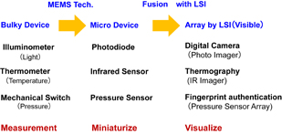
Fig. 1. Results of fusing sensor technology with LSI.
Download figure:
Standard image High-resolution imageIn the biomedical field, imaging technology has become important for understanding information obtained from organic activity. Imaging tools are an effective way to visualize information from organic matter or cells. By visualizing these phenomena, it is easy to understand them intuitively, because the eyes provide about 80% of the information entering the brain among the five senses of human beings. Imaging technology has been used in fields including agriculture, the preservation of mental and physical health, and the ion distribution associated with the activity of cells.1,2) Several kinds of ions are exchanged between the inside and outside through ion channels. To understand organic matter and/or cellular activity, ion movement through ion channels is a key issue.3)
Fluorescence microscopy is widely used in life science fields to understand many phenomena in bio-imaging. Even though fluorescence detection has the merits of sensitivity and simple handling, an imaging technique without fluorescent labels is required, to acquire understanding of the organic activity in the human body for regenerative medicine.
Several kinds of chemical microscopes with micrometer-scale resolution have been developed to obtain images of chemical species and they have been applied to biomedical systems.4) A light-addressable potentiometric sensor (LAPS) is a non-label and noninvasive microscope that uses the principle of photo generated current at an electrolyte–insulator–semiconductor structure (EIS).5) Solid-state-type bio-image sensors fusing biosensor technology with CMOS technology are attractive devices for use as bio/chemical imaging tools. These chemical imaging tools are devices that not only determine quantities, but also acquire label-free images of the local distribution of ions and chemical species in a liquid solution with real time. There are several kinds of CMOS-based bio-imaging tools. To record bioelectric potentials from neural networks, a CMOS sensor array with 128 × 128 pixels and a pixel pitch of 7.8 µm has been realized and operated at a rate more than 2000 flames/s. The CMOS sensor array successfully visualized extracellular potential images in real time.6) Amperometric detection is an attractive way to detect extra cell conditions, and an electrochemical sensor array has been fabricated.7) A potentiometric detection and amperometric detection are attractive bio-imaging applications, because they are able to detect individual information. Monolithically integrated sensor arrays for the potentiometric, amperometric, and impedimetric sensing of biomolecules have been reported.8) The imaging of ions and neurotransmitters of extracellular cells gives very useful information. High-density ion sensitive field effect transistor (ISFET) arrays for observing ion distributions,9–13) multi-DNA sequencing,14–16) and metabolite quantification have been demonstrated.17,18) In this article, we review the developments and applications of CMOS-based bio-image sensors employing a charge transfer technique.
2. Ion imaging devices
2.1. FET type ion sensors
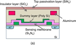
An ion detection device is an important sensor because the ion is a basic parameter in the medical and biological fields. The most well-known hydrogen ion sensor using semiconductor technology is the ISFET, which detects the variation of current through a transistor when the ion concentration changes in a solution. The ISFET for neurophysiological measurement was introduced in 197019) and many fundamental studies have been performed on these devices and various applications have been proposed.20,21) The ISFET is constructed from an ion-selective electrode (ISE) and a metal–oxide–semiconductor field-effect transistor (MOSFET). The polycrystalline silicon (poly-Si) gate electrode of a normal MOSFET is replaced by an electrolyte solution and an electrochemical reference electrode. An ion-sensitive membrane is formed on the top of the gate insulator as shown in Fig. 2. Figure 3 shows the drain current versus reference electrode-to-source voltage characteristics of an ISFET. The threshold voltage Vt shifts according to the Nernst equation, which is given by

where Vgate is the electrochemical potential between the sample solution and the ion-selective membrane, R is the gas constant, T is the absolute temperature, and F is the Faraday constant. The rate of change of Vt with respect to the pH of the sample solution depends on the material of the ion-selective membrane and is given by

where β is the sensitivity coefficient. Typical materials used for the ion-selective membrane are silicon dioxide (SiO2), silicon nitride (Si3N4), aluminum oxide (Al2O3), and tantalum oxide (Ta2O5).22–29)
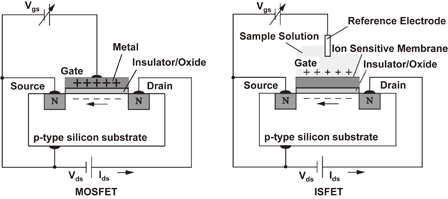
Fig. 2. Difference in structure between MOSFET and ISFET.
Download figure:
Standard image High-resolution image
Fig. 3. Output characteristics of an ISFET. The characteristic indicates drain current Ids versus reference electrode-to-source voltage Vgs.
Download figure:
Standard image High-resolution image2.2. CMOS ion image sensor based on charge transfer technique
Ion image sensors based on a charge transfer technique have been studied30,31) and applied to the field of biochemical analyses.32,33) We have developed CMOS-based ion image sensor with 32 × 32 (1 k) pixel arrangement,34) a 128 × 128 (16 k) pixel configuration,35) and a 1024 × 1024 (1 M).36) A CCD-based hydrogen ion image sensor with 1320 × 976 (1.5 M) 3.75 µm pixels was also developed.37) These sensors have achieved outputs with lower variability between each pixel than those achieved by other groups because these ion image sensors are handle electrons corresponded on an ion concentration. We believe that optical CMOS/CCD image sensors, which handle electrons, have been developed to realize low noise characteristics with a high pixel density and a small sensor size.38) An ion image sensor with a high spatial resolution, more pixels, and a higher frame rate are required for the analysis of cell membranes and the responses of neural networks.35) In this review, the fabrication of a hydrogen ion image sensor with an advanced charge transfer technique, which has a 128 × 128 pixel configuration, a high pixel density, and high frame rate is described. In order to satisfy these requirements, a specific fabrication process for an ion image sensor based on a CMOS fabrication process was developed. A new scanning method and output circuits with low output impedance were adopted to realize a higher frame rate.
2.3. Pixel configuration and sensing principle
The ion image sensor has a special pixel configuration, and an advanced readout system was adopted for the hydrogen ion sensor to achieve a higher frame rate. The pixel and readout circuits are integrated in the same chip using a modified CMOS process as shown in Fig. 4. In this subsection, the basic sensing principle is described. As shown in Fig. 5, the sensor consists of seven elements: an input diode (ID), an input control gate (ICG), an ion-sensing area, a transfer gate (TG), a floating diffusion node (FD), a reset switch, and a source follower. A Si3N4 thin film, which works as a hydrogen-ion-sensitive membrane, was deposited by thermal chemical vapor deposition (CVD) as the ion-sensing area. The sensing principle for hydrogen ions using the charge transfer technique is shown in Fig. 5. Figure 5(a) shows a cross-sectional view of a potential diagram at the time of hydrogen ion measurement in the initial stage. Figures 5(b)–5(d) show the hydrogen ion measurement procedure using the charge transfer technique. The hydrogen ions are adsorbed on a sensing membrane consisting of a Si3N4 film. The ions affect the Si surface potential in the sensor area. The ICG and TG electrodes are used to control the potential level and the gating, respectively. The ID and FD consist of pn junctions, which supply charge and detect the charge quantity. The potential level in the FD is reset as shown in Fig. 5(a). Next, the potential of the input diode decreases and electric charge flows into a potential well under the sensing part. The depth of the potential well is determined by the hydrogen ion concentration. The potential of the input gate is fixed optimally, and is determined as the lowest sensing value. The depth of the charge packet is determined by the potential difference between the control electrode and the sensing part. The input diode is initially reverse biased over the input gate potential. Next, the input diode is briefly pulsed from VD1 to VD2 [Fig. 5(b)] and then returned to VD1 [Fig. 5(c)]. In Fig. 5(c), the number of charges in the sensor area corresponds to the potential level, which varies with the hydrogen ion concentration and is maintained under the sensor area by the "fill and spill" technique.6) In Fig. 5(d), the charge is transferred to the FD by increasing the potential of the TG electrode, and the potential of the FD is also changed. An output signal is obtained from the variation of the FD potential through a source follower circuit. When the steps shown in Figs. 5(c) and 5(d) are repeated, the number of signal charges in the FD region can double. In a conventional ISFET, amplification noise decreases the signal-to-noise ratio (SNR) when amplifying output signals.39) The use of the accumulation technique for the signal charges is a major advantage of our sensor. The accumulation technique is capable of not only signal amplification but also decreasing the SNR.31,40,41) It is expected that the SNR of the pH value information increases with the accumulation of signal charges. Because the pH signal S0 is accumulated n times, the total quantity of the signal S is described as follows:

The total quantity of noise N is described as

where  are the noise components in each integration stage. If these components are the same, the above equation is simplified to

where N0 = N1 = N2 = ⋯ = Nn. Therefore, the total SNR is given by

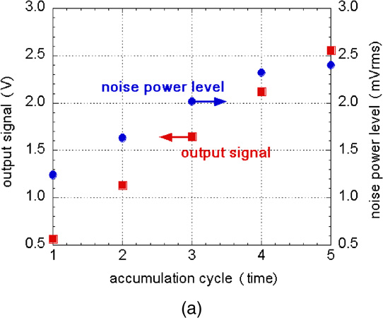
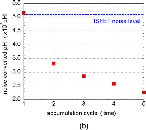
From this theoretical consideration, the SNR increases n0.5 because the signal is integrated n times. The 1/f noise component of the source follower as circuits is not influenced, because the input signals of the source follower circuit increase with the integration. The output signal and noise power level of a proposed hydrogen ion sensor employing the charge accumulation method are shown in Fig. 6(a), and the noise level of an ISFET is superimposed on it. The sampling rate of the charge-transfer-type hydrogen ion sensor was varied in the change of 1–5 Hz, depending on the accumulation cycle. However, the sampling rate was almost the same as that in the measurement of the ISFET. The output signal is proportional to the number of accumulation cycles and the noise power level increases as (gain of sensor)1/2. Thus, the noise-converted pH as input-referred value decreases with increasing number of accumulation cycles as shown in Fig. 6(b). In one accumulation cycle, noise-converted pH is 0.0052 pH, which is the same level of that of the ISFET. The noise decreases with increasing number of accumulation cycles and is 0.0023 pH after five accumulation cycles.42)
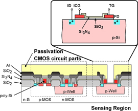
Fig. 4. Cross-sectional view of a pixel on a charge-transfer-type hydrogen ion image sensor.
Download figure:
Standard image High-resolution image
Fig. 5. Potential diagram for hydrogen ion measurement.
Download figure:
Standard image High-resolution image
Download figure:
Standard image High-resolution image
Fig. 6. Noise suppression by charge accumulation operation in charge-transfer-type ion image sensor devices. (a) Output signal and noise power level of a charge-transfer-type hydrogen ion sensor. (b) Noise-converted pH as input-referred value.
Download figure:
Standard image High-resolution image2.4. Fabrication of ion image sensors and results
2.4.1. CMOS-based hydrogen ion image sensors.
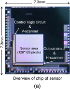
The hydrogen ion image sensor was fabricated by using a modified 0.3 µm CMOS process.35) The peripheral circuits of a timing generator and horizontal and vertical scanners are integrated onto the chip in order to reduce the size of the external operating system. Optical micrographs of the hydrogen ion image sensor chip and sensor pixel are shown in Fig. 7. The sensor area with 128 × 128 pixels was 3 × 3 mm2 area. The pixel size was 23.55 × 23.55 µm2 including the hydrogen-ion-sensing area with an exposed Si3N4 sensing membrane.
Download figure:
Standard image High-resolution image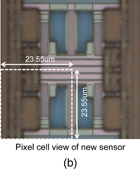
Fig. 7. Overview of the chip of the new sensor. (a) Photograph of the sensor chip. (b) Micrograph of the sensor pixels.
Download figure:
Standard image High-resolution imageA specialty fabrication process was necessary because the exposed Si3N4 membrane used as the sensing area is easily damaged by a plasma process. A fabrication process with a dummy layer for the sensor area is shown in Fig. 8. The sensing membrane consisting of a Si3N4 film is fabricated by thermal CVD in advance before a metallization process. After depositing the top passivation layer of SiNx shown in Fig. 8(a), the sensor membrane is opened using dry and wet etching. Because the Si3N4 sensing membrane was found to be damaged during the dry etching with plasma, the hydrogen ion sensitivity of the membrane was reduced. Therefore, the membrane should be opened by wet etching. The fabrication process with the dummy poly-Si layer allowed the precise control of the sensing area size. After the sensing area is covered by the poly-Si dummy layer and a top SiNx/SiOx passivation layer is deposited, the sensing area can be opened by dry etching. After the dry etching, the poly-Si layer is removed by chemical wet etching. Using the modified fabrication process, the space between the sensing area and the aluminum for wiring shown in Fig. 8(b) can be stably controlled and protected from erosion. A scanning electron microscope (SEM) which corresponds to photograph of the sensor area is shown in Fig. 9, using the part A in Fig. 8(b). Si3N4 was able to be exposed without damage by dry etching and poly-Si dummy layer.
Download figure:
Standard image High-resolution image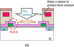
Fig. 8. Cross-sectional schematic images of the sensor area. (a) Sensor area after deposition of passivation film. (b) Sensor area after additional process for the aperture.
Download figure:
Standard image High-resolution image
Fig. 9. SEM image of sensor area, which shows the exposed hydrogen-ion-sensing Si3N4 membrane.
Download figure:
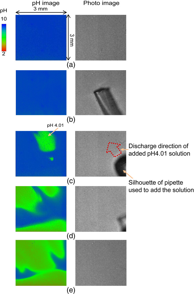
Standard image High-resolution imageFigure 10 shows atypical experimental result of real time hydrogen ion imaging by the ion image sensor chip. Snapshots of ion diffusion images and optical images taken simultaneously are shown. Firstly, a pH 9.18 solution was added to uniformly cover the surface of the chip. A uniform output signal was observed as shown in Fig. 10(a). The results indicated that the variation of the output signal among the pixels was smaller than 0.5 mV. Therefore, the sensor was capable of two dimensional hydrogen ion imaging with high accuracy. A hydrogen ion image after a pH 4.01 solution was added dropwise with a pipette is shown in Fig. 10(c). The emitted solution was discharged in the diagonal direction after its dropwise addition to the surface. Moreover, the positions of the silhouette of the pipette in the optical image and the hydrogen ion image in different areas were observed simultaneously. The images 1 s after those in Fig. 10(c) are shown in Fig. 10(d). The emitted solution diffused and spread out on the sensor area. The hydrogen ion image sensor can clearly capture the changes in the hydrogen ion distribution with a frame rate of 58 frames/s.

Fig. 10. Snapshots of ion diffusion images and optical images simultaneously taken by the hydrogen ion image sensor. (a) Initial image after dropwise addition of standard pH 9.01 solution. (b) Motion of the tip of pipette on the sensor area [5 s after image (a)]. (c) Instantaneous images showing addition of pH 4.01 solution by the pipette. (d) Images of solution with pH 4.01 diffusion [1 s after image (c)]. (e) Further diffusion of pH 4.01 solution after removing the pipette.
Download figure:
Standard image High-resolution imageThe noise suppression effect of the charge accumulation operation was confirmed. Figure 11 shows the result of measuring the pH 9.18 solution at a certain pixel for 60 s. Figure 11(a) is an image obtained under a non-accumulation condition, and Fig. 11(b) is an image obtained after ten instances of charge accumulation. There was about ±0.05 pH variability in Fig. 11(a). On the other hand, the variability was reduced to about ±0.01 pH in Fig. 11(b). We also confirmed that the standard deviation was reduced from 0.0215 to 0.0068 by the 10 instances of charge accumulation. The standard deviation decreased by a factor of  in agreement with the theoretical value. From these results, we conclude that the accuracy of our image sensor is ±0.01 (2σ) after the accumulation operation. Figure 12 shows images taken by the ion image sensor subjected to 10 instances of charge accumulation when pH 9 solution to pH 9.18 solutions. Figure 12 shows measurement result from the center pixel on the 128 × 128 image sensor. The very small shift in the pH was clearly captured.

Fig. 11. Noise suppression effect of the charge accumulation operation. (a) Image and fluctuation of output signal under non-accumulation condition. (b) Image and fluctuation of output signal after 10 instances of charge accumulation.
Download figure:
Standard image High-resolution image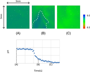
Fig. 12. Images of the ion image sensor subjected to 10 instances of charge accumulation when adding pH 9 solution to pH 9.18 solution.
Download figure:
Standard image High-resolution image2.4.2. Chemical image sensors based on hydrogen ion image sensors.
There are many ISEs for measuring various ions. Several types are categorized by the states of matter of the sensing membranes (Fig. 13), including solid, glass, and liquid types.43–46) The typical solid electrode I in Fig. 13 is a crystalline electrode. LaF3 crystal, doped with europium to improve the conductivity, is useful for measuring F−. The selective response to fluoride ions is due to the stable crystal structure of LaF3 formed on the surface of the membrane. Another useful solid ion-sensitive electrode is Ag2S. The electrode primarily responds to Ag+ and S2− and has a secondary response to Cl−, Br−, and I−. The selectivity of the electrode depends on the solubility products of the insoluble salts formed by the between their anions and silver ions. The glass electrode II has sensitivity to hydrogen ions. Molecules in a glass state are arranged more loosely and randomly than those in a normal solid, and the glass states is amorphous. While glass has little fluidity, the surface is susceptible to erosion by water. A surface based on SiO2 is easily hydrated in aqueous solutions, and the hydrated gel layer becomes responsive to hydrogen ions, similarly to in the case of Si3N4. The hydrated gel layer may respond to Na+ and K+ at their high concentrations. A commercially available Na+-selective glass ISE consists of a Na+-sensitive glass membrane. The membranes of III and IV are intrinsically liquids, which are supported by polymer or a ceramic, because a liquid cannot maintain a certain form by itself. The liquid membrane can include a mobile carrier substance that assists the selective transport of analyte ions on the liquid side of the surface. Therefore, the mobile carriers, called ionophores, produce a selective response by their alternative complexation with analyte ions. The body construction of the liquid membrane ISE can be of two types, an electrode having an inner aqueous solution inside the membrane, as in III, and a direct contact electrode without an inner solution, as in IV (coated wire electrode).47) On the former liquid membrane ISE, the inner solution includes analyte ions with a concentration of about 1 mM.
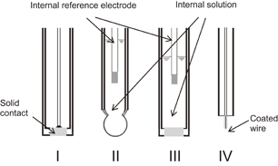
Fig. 13. Several types of ISE categorized by state of matter of sensing membrane.
Download figure:
Standard image High-resolution imageUsing the hydrogen ion image sensor as the basic device, the alteration of the ion-sensitive surface is required in order to fabricate various ion image sensors. A simple way is to place an ion-sensing membrane on the Si3N4. We used plasticized poly(vinyl chloride) (PVC) including an ionophore, similar to the coated wire electrode of IV. The usage of plasticized PVC membranes has a few advantages, they can be easily prepared on Si3N4 by casting, they can be dried without a heat process, a thin film can be made, and they can be applied to many different.
The typical plasticized PVC membrane consists of four materials, ionophore, the ion exchanger, the plasticizer as an organic solvent, and PVC as the supporting material.48) The ionophore is the most important material for selective detection of the analyte ion, and there is 1–4% of the ionophore in an ordinary membrane. It is called an ionophore-based ISE or carrier-based ISE. The ion-exchanger forms the ion-exchange site in the membrane and prevents the co-extraction of co-ions (co-ion penetration). To inhibit co-ions penetration, the ion exchanges must contain bulky lipophilic ions such as potassium tetraphenylboric acid derivatives. The ability of the inhibition depends on the amount of these ions in the membrane, and the typical amount is ∼1% in the membrane. PVC and the plasticizer account for most of the membrane content, and the ratio of the amounts of plasticizer is about 2 times PVC. In practical use, the composition of the above four materials in the membrane is optimized to selectively respond to the analyte ion.
The plasticized PVC membrane is prepared on Si3N4 by casting and drying of tetrahydrofuran (THF) solution including the above materials. Always the fabrication of the membrane is simple, problems occurred during the use of the ISE. The plasticized PVC membrane sometimes peeled off when the aqueous solution was poured onto the membrane to measure the analyte ion content. The amount of peeling off increased with the contact time of the aqueous solution. The partial peeling of the membrane reduced the potential response to the analyte ion. We improved the adhesion of the plasticized PVC membrane by the addition of polyhedral oligomeric silsesquioxanes (POSS).49) The addition of POSS was effective, and the inhibition of peeling was clearly shown by observation with a laser microscope. Moreover, the lamination of plasticized PVC with POSS improved the durability of the ion image sensor. After the use of the sensor, the ion-sensitive membrane was easily removed by only THF. In addition, the recycled sensor can be repeatedly used as another ion image sensor by laminating it with a different plasticized membrane.
We developed K+,49) Na+,50) and Ca2+ 51) sensitive ion image sensors. The K+ membrane consisted of bis(benzo-15-crown-5) as K+ ionophore, potassium tetrakis(p-chlorophenyl)borate, PVC, dioctylphthalate, and POSS as the nanofiller.49) The calibration curve of the potential difference plotted against the logarithmic K+ concentration was linear in the dynamic range from 10−5 to 10−2 M. The selectivity coefficient of K+ was 102 times higher than those of Li+ and Na+. Using the K+ ion image sensor, we monitored the leaking of the solution from a KCl-saturated Ag/AgCl reference electrode. Several snapshots captured from a movie recording the release of K+ are shown in Fig. 14. It can be seen that the high concentration of K+ spread out over the sensor with time. On the other hand, the Na+ image sensor50) can record changes in Na+ concentration with a fast response allowing the sensor to capture instantaneous changes from a high concentration to a low concentration then finally to a high concentration. Such instantaneous changes cannot be detected without a fast time constant. The Na+ image sensor tracked ion-exchange reactions on only a single bead of a Na-type cation-exchange resin. It was found that the exchange rate from Na+ to Ba2+ was two times that from Na+ to Ca2+ in the initial period of the exchange. The different rate was explained by the selectivity of the cation-exchange resin.
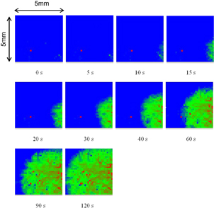
Fig. 14. Potassium ion diffusion during monitoring of KCl solution leakage from Ag/AgCl electrode.
Download figure:
Standard image High-resolution imageOn the other hand, we have also developed multi-ion image sensors which can measure two kinds of ions simultaneously.52–54) Since it was difficult to prepare the two different plasticized PVC membranes by casting, an inkjet printing method was applied to the multi-ion image sensors. An inkjet printer (IJK-200T Microjet) could finely control the printing area and the thickness of the membranes.52) The multi-ion image senor is very useful for measuring multiple types of extracellular ions simultaneously because of the several ion channels and pumps in the surface of cells. The practical application is discussed in Sect. 3.2.
3. Applications to bio-imaging
There are several routes to performing bio-imaging using hydrogen ion image sensor, which are summarized in Fig. 15. The basic technology is the hydrogen ion image sensor modified by ion-sensitive membranes and the utilization of enzymes, although it can be applied to bio-imaging even without the modification and enzymes. For instance, a 32 × 32 pixel CMOS hydrogen ion image sensor monitored the release of citric acid from a root of a rice plant as shown in Fig. 16.55) The hydrogen ion concentration around the root was observed to increase with time. The unmodified CMOS hydrogen ion image sensor may also be applied to a case in which a change in the surface potential is produced. If a certain ionic material such as DNA is adsorbed onto Si3N4, the surface charge on the substrate will be changed.32)
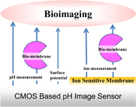
Fig. 15. Several methods of bio-imaging using CMOS hydrogen ion image sensor.
Download figure:
Standard image High-resolution image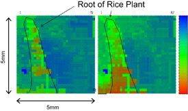
Fig. 16. Images showing the release of citric acid from the root of a rice plant taken by the hydrogen ion image sensor.
Download figure:
Standard image High-resolution image3.1. Bio-image sensors utilizing enzymes
Mechanisms of neurotransmitters have been discussed, and the findings are expected to contribute to a deep understanding of many brain functions.56–60) Acetylcholine (ACh) is an important neurotransmitter in both the central and peripheral nervous system.61) At synapses in neurons, ACh is released and chemically transmitted between neurons and networks. By using conventional optical approaches involving fluorescence probes and dyes, neurotransmitter-operated signal propagation was observed.62) The direct measurement of the two-dimensional distribution of ACh is also possible by mass spectroscopy;63) however, the cell sample should be fixed before the recording. For the real-time observation of the distribution and/or diffusion of ACh in living neurons, there are no established methods. In this section, we introduce a chemical imaging method for neurotransmitters that is based on the CMOS-type hydrogen ion image sensor.64) The distribution and diffusion of ACh were able to be visualized by combining the hydrogen ion image sensor with an ACh-sensitive layer, which consists of acetylcholine esterase (AChE) immobilized with a polyion complex33) or biotinylated AChE magnetic nano-beads.65) The developed ACh image sensor could detect the hydrogen ions generated by the ACh–AChE reaction. The enzyme-type image sensor detected a concentration change of hydrogen ions generated by the ACh–AChE enzyme reaction in accordance with the following:

Figure 17 shows the sensing principle of ACh with a hydrogen ion image sensor. The image sensor has 128 × 128 pixels in a 4.8 mm2 area.35) The surface potential of the sensing area changes with the hydrogen ion concentration, which increases after the ACh–AChE enzyme reaction. The output signal from the sensing area was proportional to the concentration of hydrogen ions generated at the ACh-sensitive layer on the sensor.
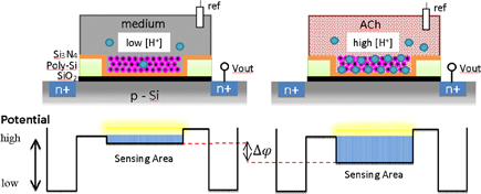
Fig. 17. Schematic potential diagram for ACh-sensing principle. AChE (violet dots) is fixed at the sensing area of an hydrogen ion image sensor. The sensor output is proportional to the concentration of hydrogen ions generated after the hydrolysis of ACh by the reaction with AChE.
Download figure:
Standard image High-resolution imageFigure 18(a) is a schematic diagram of the imaging system for ACh released from a cultured cerebral cortex. Cortical slices (approximately 400 µm thickness and 2 mm2 size) were prepared from neonatal rats, and organotypically cultured on a biomembrane.66) A slice, which was cultured for one week at 37 °C in a CO2 incubator containing 5% CO2, was placed on the hydrogen ion image sensor in a slice-side-down configuration. After recording the hydrogen ion concentration for 2 min, the cortical slice was stimulated with glutamate. As a negative control experiment, we verified in advance that the present AChE-coated hydrogen ion image sensor has no sensitivity to glutamate, which is a potent stimulator of cortical neurons. Figure 18(b) shows images of the extracellular hydrogen ion concentration in the cortical slice placed on the sensor surface. The ion concentration was slightly lower in the corresponding area when images of slices were observed by bright-field microscopy. No significant changes were observed in the extracellular hydrogen ion concentration before stimulation. In the resting state, the extracellular hydrogen ion concentration of the slice was 7.35 pH. This pH value was the average of results from three experiments. The extracellular hydrogen ion concentration gradually changed in the whole slice after stimulation with 1 mM glutamate. As shown in Fig. 19, the extracellular hydrogen ion concentration gradually decreased, and the magnitude of the decrease was more than 0.5 pH. The change is the extracellular hydrogen ion concentration was less than 0.15 pH at the outside of the slice. The decrease in the extracellular hydrogen ion concentration upon stimulation by glutamate was dependent on the presence of AChE, which generates hydrogen ions enzymatically through its reaction with ACh. These results strongly indicate that the decrease in the extracellular hydrogen ion concentration reflects the increase in the ACh concentration inside the slice. The ACh should be released from the neurons as a result of the reaction with glutamate. The continuous decrease in the extracellular hydrogen ion concentration may be caused by signal propagation in the neurons or the promotion of the ACh release. This spatiotemporal analysis of glutamate-induced ACh dynamics in a nonlabel brain slice was carried out using the bio-image sensor utilizing enzymes.

Fig. 18. Cortical slice mounted on sensor and ACh imaging of the cortical slice. The images of the extracellular hydrogen ion concentration were sequentially recorded at different times. An image of the slice was taken after 120 s of in the case of glutamate stimulation.
Download figure:
Standard image High-resolution image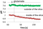
Fig. 19. Time course of extracellular hydrogen ion concentration in the glutamate-stimulated cortex. The arrow indicates the time of glutamate stimulation.
Download figure:
Standard image High-resolution image3.2. Bio-image sensors utilized chemical imaging membrane
First, we applied the K+ ion image senor to the chemical observation of a living hippocampal slice stimulated by glutamate.67) Monitoring the extracellular K+ concentration ([K+]out) of brain tissues is important for investigating physiological responses and elucidating pathological processes to cure cerebrovascular accidents or Alzheimer's disease.68,69) It is necessary to minimize the physical damage caused by operations and the chemical damage by the addition of reagents, and directly monitor [K+]out at neighboring cells. The patch clamp technique can instantly capture changes in K+ gating through ion channels;70) however, the method cannot analyze local changes in [K+]out over the whole tissue. Therefore, we developed a 128 × 128 pixels K+-sensitive image sensor with a PVC plasticized membrane including valinomycin as the K+ ionophore.
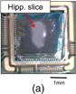
An experimental slice was prepared by cutting the hippocampus in the brain of a previously anesthetized neonatal rat. The slice was approximately 400 µm thick and had an area of 2 × 2 mm2. The slice was placed on a Millicell CM (PTFEmembrane Millipore) containing dish66) and cultured for 4 days at 37 °C with 5% CO2 air in a humidified incubator. After the culture, the slice was carefully set upside down on the K+ image sensor and filled with a recording medium [see Fig. 20(a)]. [K+]out was recorded over the entire area underneath the tissue and the surrounding area without the tissue.
Download figure:
Standard image High-resolution image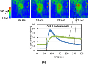
Fig. 20. (a) Optical microscope image of hippocampus slice placed on the sensor. (b) Sequential images of K ion emission from hippocampus slice placed on the sensor.
Download figure:
Standard image High-resolution image
Even before the chemical stimulation, there was a heterogeneous distribution of [K+]out in the area of the sensor. [K+]out in the surrounding area was constant and low, but underneath the tissue, a region with a slightly higher [K+]out was observed. Similar to the observation of the extracellular hydrogen ion concentration by the ion image sensor,71) the location in the tissue was illuminated via bright-field microscopy, and the area with the high [K+]out corresponded to the living tissue. After the observation before the stimulation, a chemical stimulation was performed by adding a glutamate solution to a final concentration of 1 mM to induce the depolarization of the hippocampal neurons. After the addition of glutamate, [K+]out transiently increased only under the CA1 region where the glutamate-sensitive neurons were mostly distributed,72) as shown in Fig. 20(b). [K+]out in the region was increased to more than 50 mM on average (n = 3). After reaching a peak level, [K+]out slowly decreased to the initial level after 5 min. This slow decrease in the local [K+]out may be due to either simple diffusion or ion uptake into the living cells. We thus successfully captured the chemical observation of K+ emission phenomena in the hippocampal slice. This suggests that our K+ image sensor can functionally analyze the neuronal activity of a neural network at a higher spatial resolution.
As another example of biochemical imaging, we used a Ca2+–K+ multi-ion image sensor to observe the chemical reaction of cultured rat pheochromocytoma (PC12) cells.54) Since cellular differentiation is induced by chemical stimulation, the analysis of the response of cells to the stimulation is important. When PC12 cells are treated with nerve growth factor (NGF), they differentiate into sympathetic neuronlike cells; this reaction is used to model neurosecretion.73) PC12 cells have a nicotinic ACh receptor (nAChR) that is activated by ACh.74) The nAChRs have Ca2+ permeability and are closely related to Ca2+-dependent processes.75,76) In addition, there are other ion channels called voltage-operated Ca2+ channels (VOCCs) that are opened by depolarization following the activation of nAChRs.77) When α7 nAChR is activated, Ca2+ incorporated into the cell stimulates the Ca2+ store present in the cell, and there is a mechanism that promotes the massive release of Ca2+ into the cell.78) This is called Ca2+-induced Ca2+ release (CIRCR). Thereby, when ACh stimulation is applied to suitably cultured PC 12 cells, nAChRs in the cell membrane are activated, and Ca2+ incorporated into the cells generates CICR which stimulates the Ca2+ store. The increase in [Ca2+]in by CIRCR was confirmed by fluorescence imaging.79) However, it was unknown whenever or not the event produced a change in the extracellular Ca2+ concentration. Thereby we simultaneously monitored [Ca2+]out and [K+]out, before and after the ACh stimulation of PC12 cells.
PC12 cells were grown on a poly(L-lysine) (PLL)-coated dish and incubated at 37 °C with 5% CO2 air in a humidified incubator. When the cells reached approximately 80% confluence, they were split into a collagen vitrigel membrane (CVM). Six days after the splitting into a CVM and the addition of NGF, we confirmed the elongation of the PC12 cells. The CVM with the PC12 cells was moved to the sensor surface with tweezers, and the sensor was filled with a growth medium. Using the Ca2+–K+ multi-ion image sensor, [Ca2+]out was monitored in the upper half region of the image sensor and [K+]out was monitored in the lower half region.
We started to monitor [Ca2+]out and [K+]out from 25 s before the addition of ACh solution and ended our monitoring at 300 s. Since the cells were placed between the sensor and the CVM, ACh solution slowly reached the PC12 cells by diffusing along the surface of the CVM. The results of the chemical observation showed that only [Ca2+]out was increased by the addition of ACh while [K+]out did not increase. Meanwhile, we confirmed the increase in [Ca2+]in for our cultured PC12 cells by fluorescence imaging. Thereby, it is suggested that the increase in [Ca2+]out was due to the discharge from Ca2+ channels of the activated PC12 cells. On the other hand, the lack of increase in [K+]out indicated that this stimulation was not strongly related to the absorption and release of K+ and that the chemical stimulation occurred without the collapse of cells throughout the measurement. If the collapse of cells occurred, the K+ would have been released because of the high intracellular concentration. Thus, the Ca2+–K+ multi-ion image sensor was very useful for analyzing the stimulation response of PC12 cells. The K+ ion image sensor and the Ca2+–K+ multi-ion image sensor demonstrated the exact visualization of neural activity.
4. Summary
A CMOS-based biosensor array, which is a fusion of biosensor technology with semiconductor microfabrication technology and large-scale integration technology, enables the observation of a two-dimensional chemical phenomena with high spatial and time resolution as well as sensitivity. Imaging is an effective way to intuitively understand organic activity by visualizing information obtained from organic matter or cells. This indicates that the fusion changes the role of sensors from "tools for measurement" to "tools for understanding". Bio-image sensors are strongly expected to become a valuable tool for the microbiological and medical fields and might help to discover unknown chemical phenomena in microscale structures such as single cells, cell groups, and neuronal networks.
Acknowledgments
This work was partially supported by the Adaptable and Seamless Technology Transfer Program and by the CREST program (Grant Number JPMJCR14G2) from Japan Science and Technology Agency (JST).
Biographies

Kazuaki Sawada was born in Kumamoto, Japan, in 1963. He received his B.A. and M.S. degrees in electrical and electronic engineering in 1986 and 1988, respectively, and he received a Ph.D. degree in system and information engineering in 1991, all from Toyohashi University of Technology, Aichi, Japan. From 1991 to 1998, he was a Research Associate in the Research Institute of Electronics, Shizuoka University, Shizuoka, Japan. Since 1998, he joined the Department of Electrical and Electronic Engineering, Toyohashi University of Technology, where he is now serving as a Full Professor. He is a director of Electrical and Electronics-Inspired Interdisciplinary Research Institute (EIIRIS), Toyohashi University of Technology. He was a guest professor of Technical University of Munich in 2005. His current research interests focus on the development of non label bio-image sensing devices and multimodal sensors for ion image sensing devices. He is a recipients of the Prizes for Science and Technology (Research Category), The Commendation for Science and Technology by the Minister of Education, Culture, Sports, Science and Technology of Japan 2012.

Toshiaki Hattori was born in Toyama, Japan, in 1959. He received his Doctorate of Science from Hokkaido University, Sapporo, Japan, in 1987. From 1987 to 1989, he was a Research Associate of Engineering Chemistry, Asahikawa National College of Technology, Asahikawa, Japan. In 1989, he joined Toyohashi University of Technology, Aichi, Japan, and is currently an Associate Professor of Electrical and Electronic Information Engineering.