

Abstract
A spin metal–oxide–semiconductor field-effect transistor (MOSFET) is a promising spintronics device for future low-power electronics. In this paper, we demonstrate the successful improvement of the performance of a spin-MOSFET-type device, a ferromagnetic-semiconductor GaMnAs-based vertical spin electric double-layer transistor (EDLT); the magnetoresistance ratio reaches 37%, which is 7 times larger than those obtained in previous studies. Furthermore, we find that the magnetic anisotropy of our device is modulated by changing the gate voltage. Our results open up the possibility of realizing novel functional devices, in which both current and magnetic anisotropy can be controlled by the gate electric field.
Export citation and abstract BibTeX RIS
One of the most important issues in today's electronics is to develop new devices for the postscaling era. Using spin degrees of freedom as well as charge transport of carriers, a variety of attractive spin-related phenomena and spintronics devices have been studied and proposed. Among spintronics devices proposed thus far, a spin metal–oxide–semiconductor field-effect transistor (MOSFET),1,2) in which the source and drain electrodes are ferromagnetic materials, is one of the most promising devices because it is compatible with existing well-matured semiconductor technologies and it can be applied to various fascinating applications such as reconfigurable logic circuits,3) magnetic random access memory, and nonvolatile power gating4) by utilizing magnetization-configuration-dependent output characteristics of spin MOSFETs. In previous studies on lateral spin MOSFETs,5–7) in which the drain–source current flows parallel to the plane and controlled by the gate voltage applied from the top or bottom of the channel, magnetoresistance (MR) ratios were very small (0.1%,5) 0.005%,6) and 0.027%7)). Meanwhile, a vertical spin field-effect transistor (FET), in which the drain–source current flows perpendicular to the plane and is controlled by the gate voltage applied from the side surface of the channel, is very promising because it exhibits larger MR ratios than the lateral spin MOSFETs. Previously, we showed ferromagnetic-semiconductor GaMnAs-based vertical spin FETs with large MR ratios (60%8) and 5%9)). A GaMnAs-based heterostructure is one of the most suitable material systems because we can obtain high-quality GaMnAs/semiconductor/GaMnAs trilayers, which can substantially reduce the spin relaxation during the transport.10–13) However, the current modulation ratios by the gate voltage obtained in the previous studies were not sufficient (0.5%8) and 20%9)) in the vertical spin FETs compared with those in commercially available MOSFETs (>108%). Thus, we should realize a vertical spin FET with a large current modulation ratio by the gate voltage as well as by the magnetization configuration. Furthermore, we also should control the magnetic anisotropy using the gate voltage in spin FETs because it can reduce the power consumption for writing information.
In vertical spin FETs based on GaMnAs, the gate electric field affects the electric potential profile only within ∼10 nm from the side surfaces of the intermediate channel layer because of the short channel length (9 nm).14) In this study, to increase the current modulation ratio by the gate voltage, we decreased the width of the channel down to ∼170 nm. Furthermore, we employed an ionic liquid as a gate insulator. Because the ionic liquid has an extremely higher capacitance per area (∼30 µF/cm2)15) than most solid insulators, a high current modulation ratio is expected.
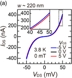
The device investigated in this study is composed of a thin GaAs layer as the channel layer and GaMnAs layers as the source and drain electrodes, and an ionic liquid as the gate insulator [Fig. 1(a)]. To form this device, which we hereafter refer to as a GaMnAs-based vertical spin electric double-layer transistor (EDLT), a heterostructure composed of, from top to bottom, Ga0.94Mn0.06As (10 nm)/GaAs (9 nm)/Ga0.94Mn0.06As (6.7 nm)/GaAs:Be (50 nm, hole concentration p = 5 × 1018 cm−3) was grown on p+-GaAs(001) substrates by low-temperature molecular beam epitaxy. After the growth, the sample was partially etched by 100 nm and a 100-nm-thick SiO2 layer was deposited in the etched area to separate the drain electrode and substrate. Then, the comb-shaped drain electrode composed of Au (40 nm)/Cr (5 nm) was formed by electron-beam lithography and a lift-off technique. Here, the width of each mesa is ∼300 nm (slightly larger than that of the final device structure). An optical microscopy image of the comb-shaped drain electrode is shown in Fig. 1(b). Next, we chemically etched the area not covered by the Au/Cr layer with phosphorous acid peroxide at 15 °C using the Au/Cr layer as a hard mask. As a result, the magnetic tunnel junctions only beneath the Au/Cr layer remained after wet etching. Owing to the nearly isotropic nature of this chemical wet etching, the width of each mesa further decreased during the etching. The estimated width w of the mesas is 170–220 nm. Finally, the device was passivated with an insulating film so that the ionic liquid covered only the gate electrode and mesas. Prior to transport measurements, we dropped an electrolyte [N,N-diethyl-N-(2-methoxyethyl)-N-methylammonium bis(trifluoromethylsulfonyl)imide (DEME-TFSI)] so that it covered the mesas and the gate electrode. After the fabricated devices were bonded with Au wires and indium solder, we measured spin-dependent transport properties with various gate–source voltage VGS values and an in-plane external magnetic field H at 3.8 K. When VGS was not applied, mobile cations and anions were randomly distributed inside the electrolyte. As a result, the electric potential in the GaAs layer was not modulated [Fig. 1(c)]. When a positive VGS was applied, mobile cations moved toward the side surfaces of the mesas, forming an electric double layer. Since it can be regarded as a nanogap capacitor, we can deplete the side surfaces of the mesas, which results in the decrease in drain–source current (by hole carriers) [Fig. 1(d)].
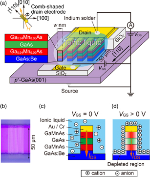
Fig. 1. (a) Schematic illustration of the vertical spin EDLT investigated in this study. The comb-shaped electrode is connected to the top of the 20 elongated mesas, where the width w of each mesa is ∼220 nm and the length of each mesa is 50 µm. Each mesa is composed of Ga0.94Mn0.06As (10 nm)/GaAs (9 nm)/Ga0.94Mn0.06As (6.7 nm)/GaAs:Be (50 nm, hole concentration p = 5 × 1018 cm−3), which is grown on a p+-GaAs(001) substrate. The back surface of the substrate is the source electrode, the top Au/Cr layer is the drain electrode, and the Au/Cr layer deposited on an insulating SiO2 film next to the mesas is the gate electrode. The gate electrode and mesas are covered with an ionic liquid (DEME-TFSI). In this figure, the insulating film used for the passivation of the device is not shown for simplicity. The configuration of the comb-shaped drain electrode and the definition of the angle ϕ of the in-plane external magnetic field H are shown at the upper left in (a). (b) Optical microscopy image of the comb-shaped drain electrode in the GaMnAs-based vertical spin EDLT. (c, d) Schematic illustration of the operation of our vertical spin EDLT when a gate voltage VGS is not applied (c) and when positive VGS is applied (d). The white region in (d) denotes the depleted region.
Download figure:
Standard image High-resolution imageTo investigate the transistor characteristics of our device, we measured the drain–source current IDS as a function of the drain–source voltage VDS with various VGS values at 3.8 K with μ0H = 0 mT, as shown in Fig. 2(a), where μ0 is the permeability of a vacuum. Here, w ≃ 220 nm. Nonlinear IDS–VDS characteristics were observed at each VGS, indicating that tunneling transport occurred. This is because GaAs is a potential barrier for holes at the Fermi level in GaMnAs.16,17) The resistance–area product (RA) was 1.34 Ω cm2 at VDS = 6 mV when VGS = 0 V. This RA is nearly the same as that in our previous paper.16) Probably because of a hysteresis character of the VGS dependence of IDS (see Sect. 1 in the online supplementary data at http://stacks.iop.org/JJAP/57/090301/mmedia), the IDS–VDS characteristics for VGS = 0 and −5 V almost overlapped with each other; i.e., IDS was not changed when VGS was decreased from 0 to −5 V; however, as shown in the inset in Fig. 2(a), we observed a clear modulation of IDS when VGS was increased to 5 V. This is a signature of the transistor operation. When VGS was changed from 0 to 5 V, the IDS modulation ratio, which is defined as [IDS(VGS) − IDS(VGS = 0 V)]/IDS(VGS = 0 V), was ∼−20% at |VDS| < 10 mV, [see the red solid curve in Fig. 2(b)]. This tendency agrees with the operation principle described in Figs. 1(c) and 1(d). In another GaMnAs-based vertical spin EDLT with w = 170 nm fabricated using a different heterostructure, we observed a more systematic and larger modulation of IDS [∼−20% (∼20%) at VGS = 4 V (−4 V)] [see Sect. 2 in the online supplementary data at http://stacks.iop.org/JJAP/57/090301/mmedia]. In Fig. 2(b), the IDS modulation ratio is decreased as |VDS| is increased. The reason for this is as follows: As |VDS| is increased, IDS flowing inside the mesa far from the side surface increases and becomes more dominant, thus the change in IDS caused by VGS becomes less dominant. The VDS dependence of the IDS modulation ratio is different from that obtained in the previous study9) probably because the qualities of the tunnel barriers are different. The possible origin of the IDS modulation is the electric field effect on the indirect tunneling current and the details are described in Ref. 14. We note that the gate leakage current is negligibly small (<100 pA).
Download figure:
Standard image High-resolution image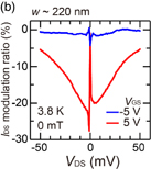
Fig. 2. (a) Drain–source current IDS as a function of the drain–source voltage VDS with VGS values of −5, 0, and 5 V in a device with w ≃ 220 nm, where VDS was changed from −50 to 50 mV in 1 mV steps. The measurement temperature was 3.8 K and the external magnetic field was not applied. The inset shows the magnified view of the region surrounded by the black dashed rectangle (40 ≤ VDS ≤ 50 mV). The drain–source current IDS vs VDS characteristic at VGS = 0 V (black curve) is invisible because it overlaps that at VGS = −5 V (blue curve). (b) IDS modulation ratio as a function of VDS with VGS values of −5 and 5 V in a device with w ≃ 220 nm at 3.8 K when μ0H = 0 mT.
Download figure:
Standard image High-resolution imageIn spin FETs, IDS should be controlled by the magnetization configuration as well as by VGS. Before the measurements, a strong magnetic field of 1 T was applied in the direction opposite to that of the in-plane magnetic field angle ϕ with respect to the [100] axis in the counter clockwise direction to align the magnetization directions of the top and bottom GaMnAs layers along the magnetic field direction [see the upper left in Fig. 1(a) for the definition of ϕ]. Then, we started to measure IDS while increasing H from zero in the direction of ϕ. As shown in Fig. 3(a), a clear tunnel magnetoresistance (TMR) was observed in our device. The TMR ratio, which is defined as [RDS(μ0H) − RDS(μ0H = 0 mT)]/RDS(μ0H = 0 mT) × 100, amounted up to 37% when ϕ was 125°. Here, RDS(μ0H) is the drain–source resistance (VDS/IDS) at H. This MR ratio is more than 7 times higher than that obtained in the previous study9) probably because of the improvement of the crystal quality of the GaMnAs layers. We also observed a minor loop, as shown by the red curve in Fig. 3(a), indicating that the antiparallel state is stable even at 0 mT. In the minor loop, the TMR ratio decreased with sweeping μ0H from −16 to 0 mT, which indicates a multidomain structure in the bottom Ga0.94Mn0.06As layer. Note that the signal observed in Fig. 3(a) originates from TMR, not from tunneling anisotropic magnetoresistance (TAMR), because the obtained anisotropy of TMR is different from that of TAMR and the signal can be well explained using the expression of TMR, as shown later.

Download figure:
Standard image High-resolution image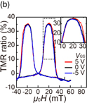
Fig. 3. (a) Drain–source resistance RDS (left axis) and the TMR ratio (right axis) as a function of μ0H at 3.8 K and ϕ = 125°, when VDS = 6 mV and VGS = 0 V. The black (red) solid line corresponds to the major (minor) loop. The black (red) arrows denote the sweep directions in the major (minor) loop. The magnetization states in the major loop are indicated by the white arrows above the graph. (b) TMR ratio as a function of μ0H applied at ϕ = 125° with various VGS values at 3.8 K, where VDS was 6 mV and VGS was varied from 5 to −5 V in 5 V steps. The inset shows the magnified view of the region surrounded by the black dashed rectangle (8 ≤ μ0H ≤ 33 mT).
Download figure:
Standard image High-resolution imageTo investigate the effect of the application of VGS on the spin-dependent transport properties, we measured major loops at ϕ = 125° with various VGS values. As shown in Fig. 3(b), the major loop was slightly modulated by VGS. When VGS was changed from 0 to 5 V, the coercive force of the top GaMnAs layer observed at μ0H = 20–30 mT increased by ∼1 mT, whereas the coercive force of the bottom GaMnAs layer observed at μ0H = 10–20 mT remained almost unchanged, as shown in the inset of Fig. 3(b). This result indicates that the ferromagnetic properties of the top GaMnAs layer are modulated by VGS. To investigate the VGS dependence of the spin-dependent transport properties in more detail, we measured the ϕ dependence of the TMR ratio with various VGS values [Figs. 4(a)–4(c)]. To obtain the ϕ dependence of the TMR ratio, the measurements were performed at every 10° step of ϕ. As shown in Figs. 4(a)–4(c), we observed mainly twofold symmetric patterns along the ![$[\bar{1}10]$](https://content.cld.iop.org/journals/1347-4065/57/9/090301/revision1/RC180022if007.gif) direction in addition to the weak fourfold symmetry along the 〈100〉 directions, and found that the anisotropy of TMR was slightly modulated by VGS. (See the experimentally obtained μ0H dependence of the TMR ratio with VGS = −5, 0, and 5 V at ϕ = 305° and VDS = 6 mV [along the white solid lines in Figs. 4(a)–4(c)] shown in Fig. 4(d)).
direction in addition to the weak fourfold symmetry along the 〈100〉 directions, and found that the anisotropy of TMR was slightly modulated by VGS. (See the experimentally obtained μ0H dependence of the TMR ratio with VGS = −5, 0, and 5 V at ϕ = 305° and VDS = 6 mV [along the white solid lines in Figs. 4(a)–4(c)] shown in Fig. 4(d)).
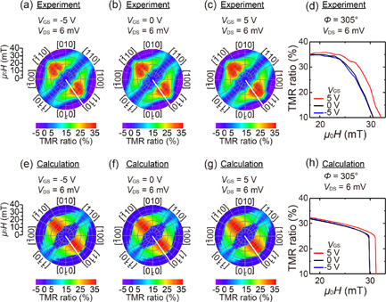
Fig. 4. (a)–(c) Experimentally obtained in-plane magnetic-field-direction dependences of the TMR ratio measured at 3.8 K with VDS of 6 mV when VGS = (a) −5, (b) 0, and (c) 5 V. (d) Experimentally obtained in-plane magnetic field dependence of the TMR ratio at ϕ = 305° with VGS = −5, 0, and 5 V when 18 ≤ μ0H ≤ 33 mT. (e)–(g) Calculated in-plane magnetic field direction dependences of the TMR ratio when VGS = (e) −5, (f) 0, and (g) 5 V. (h) Calculated in-plane magnetic field dependence of the TMR ratio at ϕ = 305° with VGS = −5, 0, and 5 V when 18 ≤ μ0H ≤ 33 mT. The white solid lines in (a)–(c) and (e)–(g) represent the magnetic field direction of ϕ = 305°.
Download figure:
Standard image High-resolution imageTo quantitatively understand the effect of VGS on the anisotropy of TMR shown in Figs. 4(a)–4(c), we reproduced the ϕ dependence of the TMR ratio using the Stoner–Wohlfarth coherent rotation model. In this model, the magnetostatic energy E of a ferromagnetic material with the magnetization M, whose in-plane direction is θ with respect to the [100] axis in the counterclockwise direction, can be expressed by9,18)
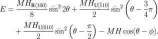
Here, HB〈100〉 is the biaxial anisotropy field along the 〈100〉 directions, ![$H_{\text{U}[\bar{1}10]}$](https://content.cld.iop.org/journals/1347-4065/57/9/090301/revision1/RC180022if008.gif) is the uniaxial anisotropy field along
is the uniaxial anisotropy field along ![$[\bar{1}10]$](https://content.cld.iop.org/journals/1347-4065/57/9/090301/revision1/RC180022if009.gif) , and HU[010] is the uniaxial anisotropy field along [010]. In this model, θ is determined so that E takes a local minimum. In addition, we introduced a domain wall nucleation/propagation energy ε; θ can move from one local minimum to another local minimum when the energy difference between these points exceeds ε. The shape anisotropy was neglected in our calculation because the magnetocrystalline anisotropy is dominant in GaMnAs. The TMR ratio can be calculated from the following equation with the relative angle Δθ of the magnetization directions of the top and bottom GaMnAs layers and the spin polarization P of the ferromagnetic layers.
, and HU[010] is the uniaxial anisotropy field along [010]. In this model, θ is determined so that E takes a local minimum. In addition, we introduced a domain wall nucleation/propagation energy ε; θ can move from one local minimum to another local minimum when the energy difference between these points exceeds ε. The shape anisotropy was neglected in our calculation because the magnetocrystalline anisotropy is dominant in GaMnAs. The TMR ratio can be calculated from the following equation with the relative angle Δθ of the magnetization directions of the top and bottom GaMnAs layers and the spin polarization P of the ferromagnetic layers.

In our calculation, P was set at 0.39 so that the maximum of the TMR ratio took 37%. Also, HU[010] was neglected because the obtained polar plots were almost symmetric with respect to the ![$[\bar{1}10]$](https://content.cld.iop.org/journals/1347-4065/57/9/090301/revision1/RC180022if010.gif) direction [Figs. 4(a)–4(c)]. As shown in Figs. 4(e)–4(g), the calculation results well reproduced the experimental data. (See the experimentally obtained μ0H dependence of the TMR ratio [Fig. 4(d)] and the calculated μ0H dependence of the TMR ratio [Fig. 4(h)] with VGS = −5, 0, and 5 V at ϕ = 305° [along the white solid lines in Figs. 4(a)–4(c) and 4(e)–4(g)] and VDS = 6 mV). By comparing the experimental data with the calculation results, we obtained the magnetic anisotropy fields (HB〈100〉 and
direction [Figs. 4(a)–4(c)]. As shown in Figs. 4(e)–4(g), the calculation results well reproduced the experimental data. (See the experimentally obtained μ0H dependence of the TMR ratio [Fig. 4(d)] and the calculated μ0H dependence of the TMR ratio [Fig. 4(h)] with VGS = −5, 0, and 5 V at ϕ = 305° [along the white solid lines in Figs. 4(a)–4(c) and 4(e)–4(g)] and VDS = 6 mV). By comparing the experimental data with the calculation results, we obtained the magnetic anisotropy fields (HB〈100〉 and ![$H_{\text{U}[\bar{1}10]}$](https://content.cld.iop.org/journals/1347-4065/57/9/090301/revision1/RC180022if011.gif) ) and ε of the top GaMnAs layer at each VGS. The obtained parameters are plotted as a function of VGS for the top GaMnAs layer in Fig. 5. As shown in the green circles in Fig. 5, ε divided by M (the magnetization of the top GaMnAs layer) was increased from 54 to 56 mT as VGS was increased from 0 to 5 V, which is the main cause of the modulation of the coercive force by VGS [inset in Fig. 3(b)]. We also found that
) and ε of the top GaMnAs layer at each VGS. The obtained parameters are plotted as a function of VGS for the top GaMnAs layer in Fig. 5. As shown in the green circles in Fig. 5, ε divided by M (the magnetization of the top GaMnAs layer) was increased from 54 to 56 mT as VGS was increased from 0 to 5 V, which is the main cause of the modulation of the coercive force by VGS [inset in Fig. 3(b)]. We also found that ![$H_{\text{U}[\bar{1}10]}$](https://content.cld.iop.org/journals/1347-4065/57/9/090301/revision1/RC180022if014.gif) in the top GaMnAs layer was slightly increased from 46 to 48 mT by changing VGS from 0 to 5 V. A recent study on the tunneling spectroscopy in GaMnAs-based diodes unveiled that the impurity band in GaMnAs shows mainly twofold symmetry along the
in the top GaMnAs layer was slightly increased from 46 to 48 mT by changing VGS from 0 to 5 V. A recent study on the tunneling spectroscopy in GaMnAs-based diodes unveiled that the impurity band in GaMnAs shows mainly twofold symmetry along the ![$[\bar{1}10]$](https://content.cld.iop.org/journals/1347-4065/57/9/090301/revision1/RC180022if015.gif) direction and that the anisotropy of the impurity band strongly depends on the energy.19) The Fermi level in GaMnAs, which is located in the impurity band,20–22) is shifted by the application of VGS via the modulation of the carrier density, and the anisotropy of the impurity band depends on the energy. These are thought to be the reasons for the modulation of
direction and that the anisotropy of the impurity band strongly depends on the energy.19) The Fermi level in GaMnAs, which is located in the impurity band,20–22) is shifted by the application of VGS via the modulation of the carrier density, and the anisotropy of the impurity band depends on the energy. These are thought to be the reasons for the modulation of ![$H_{\text{U}[\bar{1}10]}$](https://content.cld.iop.org/journals/1347-4065/57/9/090301/revision1/RC180022if016.gif) by VGS. In spite of the small depletion layer width of the top and bottom GaMnAs layers (∼3 nm), the magnetic anisotropy of the device is clearly modulated. This is because the modulation of the magnetic properties near the side surface of the top and bottom GaMnAs layers is preferentially reflected in the measured spin-dependent transport properties in our device when the conductance at the side surfaces of the mesas is tuned by VGS. In a previous study on the electric field effect for a Hallbar structure of a GaMnAs thin film, by measuring the planar Hall effect with various VGS values,
by VGS. In spite of the small depletion layer width of the top and bottom GaMnAs layers (∼3 nm), the magnetic anisotropy of the device is clearly modulated. This is because the modulation of the magnetic properties near the side surface of the top and bottom GaMnAs layers is preferentially reflected in the measured spin-dependent transport properties in our device when the conductance at the side surfaces of the mesas is tuned by VGS. In a previous study on the electric field effect for a Hallbar structure of a GaMnAs thin film, by measuring the planar Hall effect with various VGS values, ![$H_{\text{U}[\bar{1}10]}$](https://content.cld.iop.org/journals/1347-4065/57/9/090301/revision1/RC180022if017.gif) increased with decreasing VGS.23) The VGS dependence of
increased with decreasing VGS.23) The VGS dependence of ![$H_{\text{U}[\bar{1}10]}$](https://content.cld.iop.org/journals/1347-4065/57/9/090301/revision1/RC180022if018.gif) observed in our device is opposite to this previous result. This may be caused by the difference in crystal quality or by the difference in device structure (i.e., planar or vertical).
observed in our device is opposite to this previous result. This may be caused by the difference in crystal quality or by the difference in device structure (i.e., planar or vertical).

Fig. 5. Anisotropy fields (HB〈100〉 and ![$H_{\text{U}[\bar{1}10]}$](https://content.cld.iop.org/journals/1347-4065/57/9/090301/revision1/RC180022if012.gif) ) and domain wall nucleation/propagation energy ε normalized by the magnetization M as a function of VGS for the top GaMnAs layer. Here, the green circles are ε/M. The black and red circles are HB〈100〉 and
) and domain wall nucleation/propagation energy ε normalized by the magnetization M as a function of VGS for the top GaMnAs layer. Here, the green circles are ε/M. The black and red circles are HB〈100〉 and ![$H_{\text{U}[\bar{1}10]}$](https://content.cld.iop.org/journals/1347-4065/57/9/090301/revision1/RC180022if013.gif) , respectively.
, respectively.
Download figure:
Standard image High-resolution image
In summary, we have fabricated a GaMnAs-based vertical spin EDLT and investigated its spin-dependent transport properties.24) We successfully obtained the improved performance of the GaMnAs-based vertical spin EDLT in terms of magnetoresistance ratio (37%) and drain–source current modulation ratio (∼20%). The MR ratio obtained in this study is 7 times higher than those obtained in previous studies.5–7) Furthermore, we found that the in-plane anisotropy of TMR was changed by VGS. By comparing the experimental data with the calculation results, we found that ε and ![$H_{\text{U}[\bar{1}10]}$](https://content.cld.iop.org/journals/1347-4065/57/9/090301/revision1/RC180022if019.gif) were modulated by VGS. Our results suggest that gate-voltage control of the magnetic anisotropy will provide a new functionality to vertical spin FETs.
were modulated by VGS. Our results suggest that gate-voltage control of the magnetic anisotropy will provide a new functionality to vertical spin FETs.
Acknowledgements
This work was partly supported by Grants-in-Aid for Scientific Research (Nos. 26249039, 16H02095, and 18H03860) and for Specially Promoted Research (No. 25000003), the CREST Program (No. JPMJCR1777) of Japan Science and Technology Agency, and the Spintronics Research Network of Japan (Spin-RNJ). T.K. was supported by JSPS through the program for leading graduate schools (MERIT). T.K. thanks the JSPS Research Fellowship Program for Young Scientists.