
Abstract
The effects of film thickness and composition on crystal structure and dielectric properties were investigated for {111}-oriented epitaxial Pb(Mg1/3Nb2/3)O3 (PMN) and 0.6Pb(Mg1/3Nb2/3)O3–0.4PbTiO3 (0.6PMN–0.4PT) films of various thicknesses grown on (111)cSrRuO3//(111)SrTiO3 substrates by pulsed metal organic chemical vapor deposition (MOCVD). When the film thickness of {111}-oriented PMN films increased from 500 to 1300 nm, the relative dielectric constant at room temperature increased from 1600 to 2800 at 10 kHz. This tendency was similar to our previous result for {100}-oriented PMN films. On the other hand, the relative dielectric constant at room temperature slightly increased from 2500 to 2700 at 10 kHz with the increase in film thickness from 750 to 2500 nm in the case of {111}-oriented 0.6PMN–0.4PT films. PMN films show strong frequency dependences of maximum relative dielectric constant against temperature, εr(max), and the temperature of εr(max), T(max), together with a strong thickness dependence. On the other hand, 0.6PMN–0.4PT films show small frequency dependences of εr(max) and T(max) together with a small film thickness dependence. These results show a strong film composition dependence of the dielectric properties of the films in a PMN–PT system such as frequency and thickness.
Export citation and abstract BibTeX RIS
1. Introduction
Pb(Mg1/3Mb2/3)O3 (PMN) is known as a relaxor-type ferroelectric material.1–7) In bulk ceramics, it has been reported that its largest relative dielectric constant [εr(max)] and the temperature showing εr(max) [T(max)] exhibit frequency dependences.1) PMN is also an end member of the Pb(Mg1/3Nb2/3)O3–PbTiO3 (PMN–PT) solid solution system, which has been widely investigated for capacitor, inkjet-head and piezoelectric transducer applications owing to its large relative dielectric constant and piezoelectric properties near the morphotropic phase boundaries.8–18) (1 − x)PMN–xPT has a pseudo-cubic (rhombohedral) crystal structure at x < 0.3, a monoclinic crystal structure at 0.3 ≦ x ≦ 0.35, and a tetragonal crystal structure at x > 0.35.19) T(max) shifts to a higher temperature as x increases. In particular, PMN exhibits dielectric characteristics with a large frequency dependence in the temperature region below and above T(max).1)
In the case of PMN films, the relative dielectric constant at room temperature is smaller than that reported for bulk ceramics. For example, the strong film thickness dependence of the relative dielectric constant measured at room temperature was observed up to a film thickness of 2000 nm for {100}-oriented PMN films.20) On the other hand, the film thickness dependence of PbTiO3 films was reported to be small at a film thickness above 1000 nm for {100}-oriented PbTiO3 films.21) This suggests the strong PbTiO3 content, x, dependences of these characteristics. Nagarajan and coworkers reported that the dielectric and piezoelectric properties of a 0.9PMN–0.1PT thin film with a thickness of about 100 to 400 nm greatly depend on its remaining in-plane strain.22,23) However, there has been no report on the comparison of the film thickness dependence of the intermediate composition between PT and PMN films, such as 2-µm-thick 0.6PMN–0.4PT films with a maximum relative dielectric constant at room temperature.24)
In this study, we investigated the growth of epitaxial PMN and 0.6PMN–0.4PT films on (111)cSrRuO3//(111)SrTiO3 substrates of various film thicknesses and measured their dielectric properties as functions of measured temperature and frequency.
2. Experimental procedure
Epitaxial SrRuO3 films of 50 nm thickness grown on (111) SrTiO3 (STO) substrates at 750 °C by metal organic chemical vapor deposition (MOCVD) using Sr(C11H19O2)2(C8H23N5)2 (TRI Chemical Laboratory), Ru(C7H11)(C7H9) (TOSOH), and oxygen gas as sources were used as bottom electrodes.25) The pseudo-cubic Miller index of the crystal shown in brackets as (hkl)c was used for SrRuO3 (SRO). The resultant substrates were (111)cSrRuO3//(111)SrTiO3. 0.6PMN–0.4PT and PMN films of 0.5–2.8 µm thickness were grown on (111)cSrRuO3//(111)SrTiO3 substrates at 650 °C by pulsed-MOCVD. Pb(C11H19O2)2 (Kojundo Chemical Laboratory), Ti(O  i-C3H7)4 (TRI Chemical Laboratory), Mg(C14H25O2)2 (Asahi Denka), and Nb(O C2H5)5 (Asahi Denka) were used as the Pb, Ti, Mg, and Nb source materials, respectively. Oxygen was used as the oxidant gas and nitrogen as the carrier gas. The source gas mixture was allowed to flow to the substrates through a nozzle in a cold-wall-type vertical reaction chamber. The Ti/(Mg+Nb+Ti) ratio corresponding to x in (1 − x)PMN–xPT was varied by controlling the input source gas concentration under a constant Pb/(Mg+Nb+Ti) ratio of 1.00 and a Mg/(Mg+Nb) ratio of 0.33.
The crystal structure of the deposited films was investigated by X-ray diffraction (XRD; PANalytical X'Pert MRD) analysis. To characterize the electrical properties of the deposited films, 100-µm-diameter Pt top electrodes were deposited by electron-beam evaporation using a shadow metal mask. Dielectric properties were measured at room temperature using an impedance analyzer (Hewlett-Packard; 4194A). The temperature dependences of the dielectric properties were measured using a probing system (Nagase Techno-engineering; Ark-Helips-3) with a temperature-controlled stage.
3. Results and discussion
Figure 1 shows the XRD θ–2θ scans of PMN films with 500 and 1300 nm, and 0.6PMN–0.4PT films with thicknesses of 750, 1850, and 2800 nm. In all the scans, there were no peaks other than these of the {111}-oriented films and (111)cSrRuO3//(111)SrTiO3 substrates. The XRD pole figure plots measured at a fixed 2θ angle corresponding to 110 confirmed that these films were in-plane-aligned epitaxial films. This indicates that all the films shown in Fig. 1 are {111}-oriented epitaxial films.

Download figure:
Standard image High-resolution image
Fig. 1. XRD patterns of (a) PMN and (b) 0.6PMN–0.4PT films of various thicknesses grown on (111)cSrRuO3//(111)SrTiO3 substrates. The XRD pole figure plots measured at a fixed 2θ angle corresponding to 110 are also shown. SRO: SrRuO3, STO: SrTiO3.
Download figure:
Standard image High-resolution imageFigure 2 shows the thickness dependences of the lattice spacing of 111, d111, and the full width at half maximum (FWHM) of the rocking curve (ω) for the 111 diffraction peak. As shown in Fig. 2(a), the d111 values of PMN and 0.6PMN–0.4PT films were almost independent of the film thickness and were estimated to be approximately 2.33 and 2.32 Å, respectively, within the present film thickness range. This means that the remaining strain of all the films remains constant within the present study. The {111} orientation of the films is considered to be one reason for this because its remaining strain is reported to exhibit a small film thickness dependence compared with the {100} orientation in case of (Ba,Sr)TiO3 films.26) As shown in Fig. 2(b), all the films had small FWHM values below 0.6°, suggesting that they have good crystal orientation. Note that the FWHM of 0.6PMN–0.4PT films tended to gradually decrease from 0.45 to 0.4° with increasing film thickness from 750 to 2800 nm. We have already reported the crystal structure and other various properties of (1 − x)PMN–xPT thin films of 2 µm thickness grown on (100)cSRO//(100)STO, (110)cSRO//(110)STO, and (111)cSRO//(111)STO substrates.27) As a result, the PMN thin film was pseudo-cubic, while the 0.6PMN–0.4PT thin film was a mixture of pseudo-cubic and tetragonal phases. Taking into account the fact that obvious changes of XRD patterns were not detected in PMN or 0.6PMN–0.4PT films within the preset film thickness region as shown in Figs. 1 and 2, PMN and 0.6PMN–0.4PT films are considered to keep the pseudo-cubic phase and the mixture of pseudo-cubic and tetragonal phases, respectively within the present film thickness region.
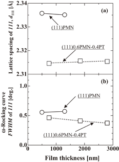
Fig. 2. Film thickness dependences of (a) lattice spacing of 111, d111, and (b) rocking curve of FWHM of 111 diffraction peak for {111}-oriented (○) PMN and (□) 0.6PMN–0.4PT films grown on (111)cSrRuO3//(111)SrTiO3 substrates.
Download figure:
Standard image High-resolution imageFigure 3 shows the film thickness dependence of the relative dielectric constant (εr) measured at 10 kHz at room temperature for {111}-oriented epitaxial PMN and 0.6PMN–0.4PT films grown on (111)cSrRuO3//(111)SrTiO3 substrates. εr increased from 1600 to 2800 with the increase in film thickness from 500 to 1300 nm. Figure 3 also shows our previously reported data of {100}-oriented epitaxial PMN films.22) The film thickness dependence trend of the εr of {111}-oriented PMN films was found to be very similar to that of {100}-oriented PMN films also shown in Fig. 3, suggesting that the film thickness dependence of εr is almost independent of the film orientation. On the other hand, εr slightly increased from 2500 to 2700 with the increase in film thickness from 750 to 2500 nm in the case of {111}-oriented 0.6PMN–0.4PT films. These results show that the film thickness dependence of εr at room temperature strongly depends on the film composition.

Fig. 3. Film thickness dependence of relative dielectric constant measured at 10 kHz for {111}-oriented (○) PMN and (□) 0.6PMN–0.4PT films together with the data of (▲) {100}-oriented PMN films.5)
Download figure:
Standard image High-resolution imageFigure 4 shows the temperature dependences of εr for {111}-oriented PMN films with thicknesses of 500 and 1300 nm, and for {111}-oriented 0.6PMN–0.4PT films with film thicknesses of 750 and 2800 nm. εr showed a maximum against the temperature for all the films. In case of {111}-oriented PMN films, T(max) varied with the measured frequency as well as with the film thickness as shown in Fig. 4(a). On the other hand, the T(max) of the {111}-oriented 0.6PMN–0.4PT film was almost constant regardless of the measured frequency. From these results, frequency dispersions were found to be reduced by increasing the PbTiO3 content x in a solid solution. Also, εr(max) at 10 kHz was found to be approximately 1950 and 3250 for the PMN film, and 3550 for the 0.6PMN–0.4PT film. These values are considerably smaller than the reported values for the single crystal, [εr(max) > 10000].1,14) This suggests the strong film thickness dependence of εr(max).

Fig. 4. Temperature dependences of relative dielectric constant for (a) {111}-oriented PMN films with thicknesses of 500 and 1300 nm, {111}-oriented 0.6PMN–0.4PT films with thickness of (b) 750 and (c) 2800 nm grown on (111)cSrRuO3//(111)SrTiO3 substrates.
Download figure:
Standard image High-resolution imageSuh et al. reported for PMN–PT ceramics that the dielectric dispersion is large in the x region below the phase transition x between the pseudo-cubic and tetragonal phases, and that the frequency dependence of T(max) decreases with the increase in x.28) On the other hand, when x is higher than this phase transition composition, PMN–PT shows a normal ferroelectric behavior (small frequency dependence). The phase transition temperature is found to be x = 0.40–0.55 for 2-µm-thick films with {100}c, {110}c, and {111}c orientations27) and the present PMN and 0.6PMN–0.4PT thin films have smaller and larger x values than the phase transition, respectively. By considering this, the present results of PMN–PT films shown in Fig. 4 are in good agreement with those of the PMN–PT ceramics in view of the frequency and temperature dependences of εr.
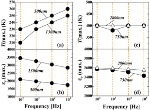
Figure 5 shows the measurement frequency dependences of T(max) and εr(max) estimated from the data shown in Fig. 4. Regardless of the film thickness, the T(max) of PMN films increased with the frequency as shown in Fig. 5(a). Note that T(max) slightly decreased with increasing film thickness for all frequencies in the case of PMN films. In our previous study, {100}-oriented PMN films basically showed the same result as {111}-oriented PMN films in the present study, suggesting a small film orientation dependence.29)
Fig. 5. Frequency dependences of (a, c) T(max) and (b, d) maximum relative dielectric constant [εr(max)] for {111}-oriented (a, b) PMN, and (c, d) {111}-oriented 0.6PMN–0.4PT films grown on (111)cSrRuO3//(111)SrTiO3 substrates.
Download figure:
Standard image High-resolution image
On the other hand, the εr(max) of PMN films tended to decrease with increasing frequency, as shown in Fig. 5(b). In addition, the εr(max) of the 1300-nm-thick film was about 1000 to 1500 higher than that of the 500 nm-thick film at all frequencies. In contrast to those of PMN films, both the T(max) and εr(max) of 0.6PMN–0.4PT films showed small frequency dependences, as shown in Figs. 5(c) and 5(d), respectively.
PMN films showed typical relaxor characteristics, indicating strong frequency dependences of εr(max) and T(max) together with a strong film thickness dependence. On the other hand, 0.6PMN–0.4PT films showed relaxor characteristics with small frequency dependences of εr(max) and T(max) together with a small film thickness dependence. These results show the strong film composition dependence of the dielectric properties of the films in a PMN–PT system, such as thickness, temperature, and frequency.
Nagarajan et al. reported that the dielectric properties of epitaxial 100–400-nm-thick 0.9PMN–0.1PT films strongly depend on the remaining in-plain strain.22) However, the obvious film thickness dependence of the crystal structure was not detected in the present study, as shown in Figs. 1 and 2. Therefore, the remaining strain effect reported by Nagarajan et al. is not considered to be the major reason for the film thickness dependence observed in the present study.23) The so-called "dead layer model" has been used to explain the film thickness dependence of the dielectric constant for ferroelectric thin films, such as Pb(Zr,Ti)O3 films, i.e., a fixed dielectric layer with a smaller dielectric constant than the upper layer exists at the interface between the bottom electrode and the ferroelectric film.30) However, the inverse capacitance was not linearly related to the film thickness for the present PMN films, in contrast to that in the dead layer model, indicating that such a model cannot explain the present results.
The present films showed smaller dielectric constants than the single crystals and sintered bodies. One possible reason for this is that the films are not clamped by the substrates. Keech et al. have recently reported the large aspect ratio dependence of the dielectric constant for the patterned PMN–PT films.31) Therefore, the measurement of the dielectric properties of the patterned PMN–PT films with different film thickness dependences is the next step in clarifying the effect of the clamp from the substrate.
The other possibility is that the domain structure of the present films is different from the those of PMN–PT ceramics and single crystals. Viehland et al. reported that relaxor-type ferroelectrics exhibit diffuse phase transitions in the vicinity of T(max) in accordance with Vogel–Fulcher's law; this is due to the polarization of B site ions with a medium- to long-range order, so called the "polar nanoregion".32) PMN and 0.6PMN–0.4PT thin films were prepared at 650 °C in the present study, which is lower than the temperature for the sintered bodies and single crystals. This means that the structures and the sizes of the polarized regions of PMN and 0.6PMN–0.4PT films can possibly be different from those of the sintered bodies and single crystals, and that the lower dielectric constants of PMN and 0.6PMN–PT thin films possibly originate from the different structures and the sizes of the polarized regions of these films. In addition, the structure and sizes of the polarized region of PMN films possibly changed with the film thickness. This is one of the origins of the film thickness dependence of the typical relaxor ferroelectric PMN films because PMN shows typical relaxor characteristics, as shown in Fig. 4(a). This can also explain the small orientation dependence because the polarized region cannot possibly exhibit an orientation dependence. On the other hand, such an effect is considered to be small in 0.6PMN–0.4PT films because these films show normal ferroelectric characteristics, as shown in Figs. 4(b) and 4(c). In such a case, the film thickness dependence can be small because the film thickness region of the present study is above 500 nm.
The detailed observation of the microstructure including the domain structure by transmission electron microscopy (TEM) and piezo-response force microscopy (PFM) is the next step of the present study. In addition, postannealing treatment can possibly change the microstructure and dielectric properties of 0.6PMN–0.4PT films.
4. Conclusions
The effects of film thickness and composition on crystal structure and dielectric properties were investigated for {111}-oriented epitaxial PMN and 0.6PMN–0.4PT films of various thicknesses grown on (111)cSrRuO3//(111)SrTiO3 substrates by pulsed-MOCVD. εr increased with the increase in film thickness from 500 to 1300 nm for PMN films. On the other hand, εr at room temperature slightly increased from 2500 to 2700 with the increase in film thickness from 750 to 2500 nm in the case of 0.6PMN–0.4PT films. These results show that the film thickness dependence of εr at room temperature strongly depends on the film composition. PMN films show strong frequency dependences of εr(max) and T(max) together with a strong film thickness dependence. In contrast, 0.6PMN–0.4PT films show small frequency dependences of εr(max) and T(max) together with a small film thickness dependence. These results show the strong film composition dependence of the dielectric properties of the films in a PMN–PT system, such as thickness, temperature, and frequency.
Acknowledgement
This work was supported by JSPS KAKENHI Grant Numbers 26220907 and 15H04121.
Biographies

Shoji Okamoto is a doctoral course student of Department of Innovative and Engineered Materials, Tokyo Institute of Technology from 2015. He received the master degree from Tokyo Institute of Technology in 2005. And he joins the company from 2005. He has published 34 papers in refereed international journals.
Satoshi Okamoto is a former student of Department of Innovative and Engineered Materials, Tokyo Institute of Technology. He received the master degree from Tokyo Institute of Technology. In 2006, he joins the company. He has published eight papers in refereed international journals.
Shintaro Yokoyama is a former student of Department of Innovative and Engineered Materials, Tokyo Institute of Technology. He received the Ph.D. degree from Tokyo Institute of Technology in 2006. He has published 60 papers in refereed international journals.

Hiroshi Funakubo is a professor of Department of Innovative and Engineered Materials, and Department of Materials Science and Engineering Tokyo Institute of Technology. He received the Ph.D. degree from Tokyo Institute of Technology. In 1989, he was an assistant professor in the Faculty of Engineering, Tokyo Institute of Technology. In 1997 and 2012, he has been an associate professor and full professor of Interdisciplinary graduate school of Science and Technology, Department of Innovative and Engineering Materials, Tokyo Institute of Technology. His recent research focuses on preparation and properties of dielectric, ferroelectric and piezoelectric films. He has published over 600 papers in refereed international journals.