
Abstract
We demonstrate a significant improvement in the epitaxial growth of perovskite dielectric films on MgO by introducing a SrTiO3 (STO)/TiO2 buffer layer, which enhances their dielectric response. 270-nm-thick (001)-epitaxial (Ba,Sr)TiO3 (BST) films were deposited by pulsed laser deposition on STO/TiO2-buffered MgO with a SrRuO3 (SRO) bottom electrode. The film directly deposited on SRO/MgO grew in a three-dimensional mode, resulting in a rough and poorly crystalline film with an almost relaxed strain. On the other hand, the film with a buffer layer grew in a two-dimensional mode, resulting in a flat and highly crystalline film with a large compressive strain (−0.80%). As a result, the paraelectric-to-ferroelectric phase transition temperature increased by 220 °C and an out-of-plane dielectric constant exceeding 1000 was achieved.
Export citation and abstract BibTeX RIS
1. Introduction
MgO is a promising substrate material for dielectric and ferroelectric thin film devices from both physical and practical points of view. For the former, MgO has a low optical index (n = 1.71 at λ = 1595.2 nm)1) and thus can serve as a good cladding layer for optical waveguides in ferroelectric electro-optic devices.2–5) It also has a low dielectric constant and a low dielectric loss (εr ≈ 10 and tan δ ≈ 5 × 10⁻⁶ at 10.48 GHz),6) which are suitable for tunable dielectric devices.7) For the latter, MgO is widely available commercially and inexpensive compared with other various single crystal substrates. However, in contrast to these merits, the large differences in crystal structure and lattice constant with respect to most dielectric, ferroelectric and electrode materials with a perovskite structure are a serious issue. Therefore, it is difficult to achieve film growth while maintaining a flat surface and a high crystallinity.8–10)
Thus far, several attempts to grow high-quality epitaxial dielectric and ferroelectric films on MgO have been reported. However, most works have focused on the improvement in in-plane dielectric properties.9–17) The improvement in out-of-plane properties (namely, in the thickness direction) is more difficult as high-temperature deposition and annealing are limited owing to the inter diffusion between the film and the underlying electrode.18) Furthermore, it is well known that the out-of-plane dielectric constant decreases with decreasing film thickness so that it is difficult to achieve a large out-of-plane dielectric constant with thinner films.18–20) A good example is (Ba,Sr)TiO3 (BST) films. The maximum dielectric constant measured as a function of temperature for BST films with thicknesses less than 300 nm has been reported to be 60209) and 60019) for the in-plane and out-of-plane directions, respectively; the out-of-plane values are only 1/10 of the in-plane values.
In this paper, we report a markedly enhanced out-of-plane dielectric constant for (Ba0.7Sr0.3)TiO3 thin films on MgO, brought about by the improvement in film growth. By introducing a thin SrTiO3 (STO)/TiO2 buffer layer between the SrRuO3 (SRO) bottom electrode and the MgO substrate, a highly crystallized 270-nm-thick BST film grew in a two-dimensional mode with compressive strain, which gave rise to a maximum dielectric constant exceeding 1000 at an elevated paraelectric-to-ferroelectric phase transition temperature.
The strategy to grow a high-quality BST film on MgO with a bottom electrode is as follows. On MgO(001) surfaces, the AO plane of ABO3-type perovskite is unstable as either the cation Ax+ or anion O2− in the AO plane should be placed on Mg2+ or O2−; namely, ions with charges of the same sign are close to each other. On the other hand, in the case of the BO2 plane on MgO, the cation By+ and anion O2− can respectively be placed on O2− and Mg2+ ions with charges of opposite signs, which can reduce the interfacial energy between ABO3-type perovskite and MgO.21–23) Mckee et al. reported that the epitaxy of BaTiO3 films on MgO was enhanced when the deposition started from a TiO2 atomic layer by molecular beam epitaxy.23) In the present study, we deposited 1 monolayer (ML) of TiO2 (equivalent to a single BO2 layer in the ABO3-type perovskite lattice) followed by a thin STO layer on MgO by pulsed laser deposition (PLD). This STO/TiO2 layer provides a flat perovskite surface, which acts as a buffer layer suitable for the following epitaxial growth of the perovskite SRO bottom electrode layer and BST film.
2. Experimental methods
All layers including BST, SRO, STO, and TiO2 were deposited by PLD with a KrF excimer laser (λ = 248 nm). A ceramic pellet of (Ba0.7Sr0.3)TiO3 prepared by a standard sintering process, a commercial ceramic pellet of SRO, and commercial single crystals of STO and TiO2 were used as targets for PLD. The laser energy and repetition rate were 60 mJ and 2–7 Hz, respectively. 1 ML of TiO2 was deposited on a polished MgO substrate at 600 °C in 0.5 mTorr O2 and then a 10-nm-thick STO layer was deposited at 750 °C under the same O2 pressure. Following the deposition of a 50-nm-thick SRO electrode layer at 700 °C in 200 mTorr O2, a 270-nm-thick BST thin film was deposited at 700 °C in 10 mTorr O2. For comparison, BST and SRO were also deposited on MgO(001) without a STO/TiO2 buffer layer. After depositing BST films, circular platinum top electrodes of 100 µm diameter and 50 nm thickness were fabricated by electron beam evaporation.
The crystal structure and orientation of the fabricated BST films were characterized by X-ray diffraction (XRD) using a four-axis diffractometer with Cu Kα1 X-rays (Bruker D8 DISCOVER). The surface morphology was observed by atomic force microscopy (AFM; Asylum Research MFP-3D) and reflection high-energy electron diffraction (RHEED; Pascal). A precision LCR meter (Keysight E4980A) and a temperature controller (MMR K-20) were used to investigate the dielectric properties of the BST films in the frequency range of 1–10 kHz and in the temperature range of −191 to 307 °C.
3. Results and discussion
Figure 1 shows XRD 2θ/ω patterns around BST 002 and SRO 002 for BST films deposited on a SRO electrode on MgO with and without a STO/TiO2 buffer layer. Both BST films had a perovskite structure without any secondary phases and a perfect (001) orientation along the substrate normal direction. However, BST and SRO peaks for the sample with a STO/TiO2 buffer layer are located at slightly lower angles than those without a buffer layer, implying a different residual strain state, and hence growth behavior, between the two samples. To clarify the growth behavior of these films, RHEED images were acquired at each deposition step.
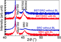
Fig. 1. XRD 2θ/ω patterns around BST 002 and SRO 002 for BST films deposited on a SRO electrode on MgO with and without a STO/TiO2 buffer layer (BL). The pseudo-cubic Miller index is used for SRO. The patterns before BST deposition are also plotted.
Download figure:
Standard image High-resolution imageFigure 2 shows RHEED patterns of the STO/TiO2 buffer layer on MgO along the MgO[100] azimuth. The initial sharp streaky pattern of MgO indicates a flat surface. After the deposition of 1 ML of TiO2, the streaky features were maintained.24) The following STO layer showed clear streaks at 0, 1 and 0, 2, indicating a flat STO surface with a STO[100] ∥ MgO[100] epitaxial relationship. A similar epitaxial growth of STO on a TiO2-truncated MgO surface was reported by McMitchell and coworkers.25–27) Note that, during the STO deposition, the in-plane lattice constant of the growing STO surface estimated by in situ RHEED observation rapidly decreased and became closer to the unstrained value at the deposition temperature [see Fig. 2(d)], which indicates that the almost relaxed flat STO layer was formed on MgO.
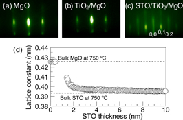
Fig. 2. RHEED patterns of a STO/TiO2 buffer layer on MgO along the MgO[100] azimuth: (a) initial MgO, (b) after deposition of 1 ML of TiO2, and (c) after 10-nm-thick STO deposition. (d) shows the change in the in-plane lattice constant of the growing STO surface estimated by in situ RHEED observation.
Download figure:
Standard image High-resolution imageFigure 3 shows RHEED patterns of the films with and without a buffer layer. In the case of the film without a buffer layer, the SRO layer deposited on MgO showed a slightly diffused spotty pattern, indicating the three-dimensional growth of SRO with low crystallinity. After BST deposition, a diffused spotty pattern similar to that of the SRO layer was observed. Such three-dimensional growth of BST films on MgO under standard PLD conditions has often been reported.10,28) In contrast, when SRO and BST films were deposited on MgO with a STO/TiO2 buffer layer, the growth behavior was notably different. The streaky pattern of the STO/TiO2 buffer layer was maintained after the SRO and BST depositions, indicating the growth of flat epitaxial BST/SRO films on STO as a buffer layer, similar to that of the well-known epitaxial BST/SRO films on STO single crystals.29) The observed difference in the growth behavior of the films on MgO with and without a STO/TiO2 buffer layer was further confirmed by XRD and AFM.
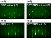
Fig. 3. RHEED patterns of SRO layers (1) and BST films (2) deposited on MgO along the MgO[100] azimuth: (a) without and (b) with a STO/TiO2 buffer layer (BL).
Download figure:
Standard image High-resolution imageFigure 4 shows XRD ω scans, i.e., rocking curves, for the BST 002 of the films. The full widths at half maximum (FWHM) of the films with and without a buffer layer were 0.97 and 2.77°, respectively, indicating the significant enhancement of the crystallinity of the BST film upon the introduction of the STO/TiO2 buffer layer. Figure 5 shows AFM images of the SRO and BST surfaces. The root mean square (RMS) surface roughnesses estimated from a 2 × 2 µm2 area are listed in Table I. Compared with the SRO layer directly deposited on MgO, the SRO layer on STO/TiO2-buffered MgO had a smoother surface and larger grains. These characteristics were also inherited to the upper BST film.
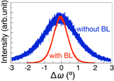
Fig. 4. XRD ω scans for BST 002 of BST films deposited on a SRO electrode on MgO with and without a STO/TiO2 buffer layer (BL).
Download figure:
Standard image High-resolution image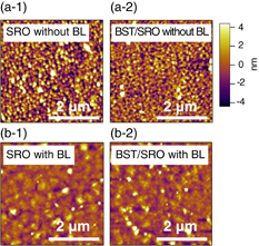
Fig. 5. AFM images (2 × 2 µm2) of SRO layers (1) and BST films (2) deposited on MgO: (a) without and (b) with a STO/TiO2 buffer layer (BL).
Download figure:
Standard image High-resolution imageTable I. RMS surface roughness values (in nm) estimated from 2 × 2 µm2 AFM scans for SRO electrode layers and the following BST films deposited on MgO with and without a STO/TiO2 buffer layer (BL).
| SRO | BST | |
|---|---|---|
| Without BL | 2.18 | 1.87 |
| With BL | 1.11 | 1.39 |
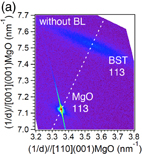
Since the STO/TiO2 buffer layer provides a flat perovskite surface, the upper SRO and BST films can easily be subjected to lattice mismatch with STO. Figure 6 shows XRD reciprocal space maps around BST 113 for the films with and without a buffer layer at room temperature. The BST film without a buffer layer was almost relaxed, whereas that with a buffer layer had a large in-plane compressive strain of −0.80% at room temperature. To experimentally confirm the origin of this strain, the temperature dependence of the lattice constant was measured, as shown in Fig. 7. The film without a buffer layer showed a monotonic increase in out-of-plane lattice constant with increasing temperature, which is in good agreement with the slope estimated on the basis of the assumption that the in-plane lattice constant follows the thermal expansion of the MgO substrate.30) On the other hand, for the film with a buffer layer, the out-of-plane lattice constant first decreased and then increased with increasing temperature, indicating that the film was in the ferroelectric phase at around room temperature. In addition, unlike the film without a buffer layer, the in-plane lattice constant extrapolated to the deposition temperature is appreciably smaller than the out-of-plane value, which indicates that the film was under the compressive stress during the deposition because of the lattice mismatch with the underlying SRO/STO. Although the thickness of the BST film was much larger than the critical thickness for misfit dislocations on SRO/STO,31) the two-dimensional growth of BST significantly delayed the strain relaxation from the lattice mismatch.29)
Download figure:
Standard image High-resolution image
Fig. 6. XRD reciprocal space maps around BST 113 for the films (a) without and (b) with a STO/TiO2 buffer layer (BL). Dashed lines correspond to cubic lattices.
Download figure:
Standard image High-resolution image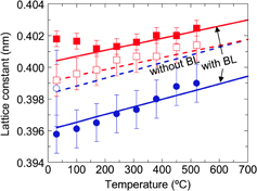
Fig. 7. Temperature dependence of in-plane (○, ●) and out-of-plane (□, ■) lattice constants of BST films without (○, □) and with (●, ■) a STO/TiO2 buffer layer (BL). The slopes estimated on the basis of the assumption that the in-plane lattice constant follows the thermal expansion of the MgO substrate are also plotted by dashed and solid lines for the films without and with a BL, respectively.
Download figure:
Standard image High-resolution imageThe film with a buffer layer having compressive strain showed a markedly enhanced dielectric response. Figure 8 shows the temperature dependences of the dielectric constant εr and dielectric loss tan δ for the films with and without a buffer layer. The experimentally determined paraelectric-to-ferroelectric phase transition temperature T0 values, at which εr peaked, were 247 and 23 °C for the films with and without a buffer layer, respectively. The T0 of the unstrained bulk Ba0.7Sr0.3TiO3 is known to be 27 °C,32) which is close to that for the almost relaxed film without a buffer layer. On the other hand, the compressively strained film with a buffer layer showed a higher T0 > 200 °C. Indeed, the film with a buffer layer showed a saturated P–E hysteresis loop at room temperature (not shown here), clearly indicating its ferroelectric nature below the enhanced T0. In contrast, such a saturated P–E hysteresis loop was not observed for the film without a buffer layer at any examined temperatures below T0 owing to the large leakage current.

Fig. 8. Temperature dependences of εr and tan δ for the films with and without a buffer layer (BL). The experimentally observed T0 values, at which εr peaked, are shown by solid lines. In addition, the theoretically predicted T0 values from the measured strain are shown by dashed lines.
Download figure:
Standard image High-resolution image
The increase in T0 by compressive strain can be predicted as
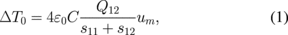
where ε0 is the permittivity of vacuum, and C, Qij, sij, and um are the Curie–Weiss constant, the electrostrictive coefficient, the elastic compliance, and the in-plane strain of BST, respectively.31) As can be seen in Fig. 8, the theoretically predicted T0 roughly agreed with the observations. In addition to the shift in phase transition temperature, the film with a buffer layer clearly showed a sharper, higher peak of the dielectric constant. As a result, the maximum dielectric constant exceeded 1000, although there is some relaxor-like frequency dispersion, as similarly observed in highly strained STO films.33,34) To the best of our knowledge, the out-of-plane dielectric constant observed in the BST film with a STO/TiO2 buffer layer on MgO is significantly higher than the previously reported out-of-plane dielectric constants of BST films on MgO with a similar thickness less than 300 nm.19) The enhanced dielectric constant can be attributed to the improvement in the crystallinity of the BST film by introducing a STO/TiO2 buffer layer.
4. Conclusions
We demonstrated a novel approach to growing highly crystalline flat epitaxial BST films with SRO bottom electrodes on MgO by introducing a STO/TiO2 buffer layer. The flat STO surface formed on MgO acts as a suitable buffer layer for the epitaxial growth of perovskite SRO and BST films in a two-dimensional mode. The BST film was compressively strained owing to the lattice mismatch with the SRO/STO buffer layer, resulting in a significantly higher paraelectric-to-ferroelectric phase transition temperature. The improved crystallinity increased the maximum out-of-plane dielectric constant above 1000. The employed approach can also be applied to other functional perovskite dielectric and ferroelectric materials for future emerging applications.
Acknowledgment
This work was partly supported by the Concert-Japan Project "FF-Photon" from the Japan Science and Technology Agency.
Biographies

Shinya Kondo was born in Japan. He received his M.S. degree in Materials, Physics, and Energy Engineering from Nagoya University, Nagoya, Japan, in 2017. In 2015, he shortly stayed at the Ceramics Laboratory, École Polytechnique Fédérale de Lausanne, Lausanne, Switzerland to develop a phenomenological theory of the electrooptic effect in strained ferroelectric films and participated in the CONCERT-Japan: FF-Photon project. He is currently a Ph.D. student of Department of Energy Engineering in Nagoya University. His current research interests include ferroelectric thin films with focus on heteroepitaxial growth and electrooptic properties.

Tomoaki Yamada received his B.S. degree in Inorganic Materials and his Ph.D. degree in Materials Science and Engineering from the Tokyo Institute of Technology, Tokyo, Japan, in 1999 and 2003, respectively. In 2004, he joined the Ceramics Laboratory, École Polytechnique Fédérale de Lausanne, Switzerland, as a postdoctoral researcher. In 2008, he became an Assistant Professor at the Tokyo Institute of Technology. In 2010, he moved to the Nagoya University, Nagoya, Japan, as an Associate Professor. His current research interests include functional metal oxide thin films and devices with focus on the manipulation of epitaxial growth and applications of these heterostructures.

Masahito Yoshino received his B.S. and Ph.D. degrees in Materials Science and Engineering from Nagoya University, Nagoya, Japan, in 1998 and 2003, respectively. He is currently an Assistant Professor of Nagoya University. His current research interests include first principles calculation, synthesis, and characterization of oxide materials (e.g., perovskite-type oxides and pyrochlore-type oxides) as electronic and luminescent materials.

Takanori Nagasaki was born in Japan. He received his M.Eng. and D.Eng. degrees in Nuclear Engineering from the University of Tokyo, Tokyo, Japan, in 1983 and 1993, respectively. He was involved in research on nuclear fusion materials at the Japan Atomic Energy Research Institute, Tokai, Ibaraki, Japan, from 1983 to 1995. In 1991, he was with Cambridge University, Cambridge, U.K., as a Visiting Scholar. Since 1995, he has been an Associate Professor and a Professor of Nagoya University, Nagoya, Japan. His current research interests include energy-related materials, especially those materials used in the hydrogen energy system.