
Abstract
Electrically controllable antiferromagnets will play a prominent role in the development of future spintronics. These materials offer a way to realize innovative low-energy-consumption, high-speed, highly integrated spintronic devices for storage, memory, and logic use. The magnetoelectric manipulation of antiferromagnetic spin in Cr2O3 is one of the most promising ways to achieve such devices. Crucial problems toward device applications are 1) the establishment of high-quality Cr2O3 thin-film fabrication techniques and the demonstration of the adaptability of such films for high-performance devices, and 2) the enhancement of the operating temperature in order to ensure sufficient stability for room-temperature operations. In this review, we summarize the recent progress made in Cr2O3 thin-film research, especially focusing on the magnetoelectric manipulation of antiferromagnetic spin and material development for achieving a higher operating temperature in Cr2O3 thin films.
Export citation and abstract BibTeX RIS
1. Introduction
Magnetoelectric antiferromagnets (ME-AFMs) have been attracting attention for use in high-performance future spintronic device applications since their prediction by Curie.1) AFMs have been recognized to be superior to ferromagnets (FMs) as they have THz resonance frequency, do not generate stray fields, and are stable in the presence of an external magnetic field.2–4) The ME effect allows the electric manipulation of the magnetic properties. By combining these benefits, it is expected that electrically controllable, ultralow-energy-consumption, ultrahigh-speed, and highly integrated nonvolatile devices for data processing can be realized. Ultralow energy consumption is a highly expected feature for future data-processing devices, since the huge energy consumption reflecting the rapid increase in processing data is becoming a serious problem. ME-AFMs do not have the specific weak points of FM-based spintronic materials, such as device-incompatible magnetic-field writing and magnetic interference; thus, they are more compatible with semiconductor-based data-processing devices. Such compatibility would be a major benefit of using AFMs in addition to the high performance expected.
Cr2O3 is a prototype ME-AFM, for which Dzyaloshinskii proposed linear ME properties in 1960,5) and soon after that, it was experimentally demonstrated by Astrov.6,7) Figure 1 depicts the two equivalent antiferromagnetic domains of Cr2O3. The Cr spin aligns antiferromagnetically as ↑↓↑↓ or ↓↑↓↑ along the crystalline c-axis within the magnetic unit cell. Due to the breaking of time- and space-inversion symmetries, Cr2O3 exhibits ME effects. The electric field parallel to the c-axis destroys the inversion symmetry, creates a difference in absolute magnitude between the up- and down-spin sublattices, and produces a net magnetization. Such electric field (E)-induced magnetization (inverse ME effect)6–13) and magnetic field (H)-induced electric polarization (normal ME effect)14–17) were demonstrated in sequence. In addition, antiferromagnetic spin reversal by the simultaneous application of E and H was also demonstrated.18–20) The free energy per unit volume of Cr2O3 with ↑↓↑↓ (↓↑↓↑) spin alignment, F+ (F−), in the presence of both E and H can be written as18)

where χ is the magnetic susceptibility, χ' is the electric susceptibility, and α is the ME susceptibility. The ME susceptibility α has both parallel (α∥) and perpendicular (α⊥) components along the c-axis; however, in this paper, we deal only with parallel components, thus α ≡ α∥. In the presence of both E and H, an energy difference of ΔF = 2αEiHj exists between the two antiferromagnetic spin alignments. Thus, the application of parallel E and H stabilizes the ↑↓↑↓-type antiferromagnetic domain, whereas the application of antiparallel E and H stabilizes the ↓↑↓↑-type antiferromagnetic domain. Nonvolatile ME manipulation can be achieved by using the antiferromagnetic domain switching using linear ME effects. Since the driving force of such antiferromagnetic domain switching is the energy difference ΔF = 2αEiHj, a larger α makes the switching more efficient. However, near room temperature, such antiferromagnetic domain switching has not been realized for other ME materials. In particular, there are no reports of antiferromagnetic domain switching by the ME effect for composite ME materials despite them exhibiting much larger α than Cr2O3.21,22) This is due to the lack of an observation of the inverse ME effect (E-induced magnetization) in these systems. Since the relative direction of the applied E and H is important for antiferromagnetic domain switching, if we apply a constant H, the antiferromagnetic domain can be switched by changing the direction of the applied E, as shown in Fig. 1. While the ME effect of Cr2O3 was demonstrated as early as the 1960s, this phenomenon was not used for practical applications owing to the difficulty encountered in the practical detection of antiferromagnetic spin. The situation changed in 2005, when Borisov et al.23) demonstrated the ME switching of exchange bias. They detected the switching of an antiferromagnetic single domain from a neighbor FM through the exchange bias. This was the starting point of extensive research based on ME-AFM Cr2O3 aiming at spintronic applications, which led to several proposals of futuristic spintronic devices for storage, memory, and logic use.24–32)
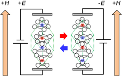
Fig. 1. Scheme of ME manipulation of antiferromagnetic domain in Cr2O3. By changing the electric field direction only, a different antiferromagnetic domain state (↑↓↑↓ or ↓↑↓↑) is stabilized.
Download figure:
Standard image High-resolution imageRecently, the nonvolatile electric manipulation of FMs has received increasing attention,33) reflecting the demand for ultralow-energy-consumption data-processing devices. However, only few possible materials remain for the realization of nonvolatile 180° switching of the ferromagnetic moment by electrical means. The multiferroic AFM BiFeO3/FM system is one of these. It can achieve the electric switching of exchange bias34,35) because the antiferromagnetic spin of BiFeO3 rotates accompanied with the ferroelectric polarization when it is reversed by an electric field. BiFeO3 can achieve purely electric control of antiferromagnetic spin without any magnetic field, which is one of the main characteristics of such a system. However, the different directions of the antiferromagnetic spin and electric polarization would be a drawback of using BiFeO3. In the BiFeO3/FM system, the reversal of in-plane exchange bias was realized by applying a perpendicular electric field.35) Another promising possibility is the dynamic magnetization switching of a ferromagnetic metal/oxide system by a voltage pulse,36,37) in which the voltage control of the magnetic anisotropy (VCMA) effect is used. In this case, ultrafast switching of FM (on the order of sub-ns) in a magnetic tunnel junction (MTJ) is possible, whereas deterministic switching cannot be achieved. In contrast to these systems, 180° deterministic switching of a perpendicular exchange bias can be realized in a Cr2O3/FM system by exploiting its linear ME effect. Since Cr2O3 is a paraelectric material, the application of both E and H is required to obtain antiferromagnetic spin switching. However, a constant permanent magnetic field can be generated by incorporating a hard-magnetic bottom layer.27)
For the Cr2O3/FM systems, the demonstration of robust isothermal electric control of the exchange bias at room temperature by He et al. in 201038) made the prospect of device applications more realistic. However, the demonstration was performed using a Cr2O3 single-crystal substrate with a thickness in the range of 0.5–0.7 mm. In order to demonstrate the effectiveness for device applications, ME manipulation must be reproduced in a Cr2O3 thin film. Therefore, since the initial findings in 2005, the magnetic properties of Cr2O3 thin films have been intensively studied. In particular, the perpendicular exchange bias in Cr2O3/FM all-thin-film systems has been extensively investigated and its unique properties have been clarified.39–75) However, until very recently, the ME manipulation of antiferromagnetic domains has not been demonstrated in an all-thin-film system. Another challenge for device applications is operating-temperature engineering. While ME manipulation of the exchange bias has been demonstrated at room temperature (303 K),38) the Néel temperature of Cr2O3 (TN ∼ 307 K) is insufficient for practical device applications. TN must be increased by at least 50 K to withstand the operating environment. The small magnetic anisotropy of Cr2O3 (KAF ∼ 2 × 10⁵ erg/cm3)76) also degrades the operating temperature. In the Cr2O3/FM exchange bias system, the exchange bias was observed only at significantly lower temperatures than TN;45,48,50,51,55–59,63,72,77) this is because the small magnetic anisotropy of Cr2O3 cannot sustain the large exchange bias and cannot fix the FM, which is explained by Meiklejohn and Bean's model (MB model).45,78,79) Thus, an increase in the magnetic anisotropy is also required to increase the operating temperature.
In this paper, we review the recent progress made in Cr2O3 thin-film research. In particular, we focus on the realization of the ME manipulation of antiferromagnetic domains in a Cr2O3 all-thin-film system and attempt to achieve a higher operating temperature in a Cr2O3 film. In Sect. 2, we will show the ME manipulation of an antiferromagnetic domain in a Cr2O3 all-thin-film system by using both the ME field cooling (MEFC) process32,63,80–83) and the isothermal process.63,84–87) The usage of all-thin-film systems will be beneficial not only for downsizing devices and reducing the operation voltage but also to deeply understand the underlying physics, because the use of a thin film enables better control of the stacked structures and interfaces. Moreover, a thin-film process will allow further material developments of Cr2O3 and the possibility of discovering new functionalities. In Sect. 3, we will summarize the recent research on the operating temperature of Cr2O3 films. While TN engineering is a difficult task, there are several possibilities for achieving TN > 350 K. Progress has also been made in enhancing magnetic anisotropy; as will be described in this paper, sufficient magnetic anisotropy can be achieved by lattice strain engineering and doping.
2. Magnetoelectric manipulation in Cr2O3 thin film
In this section, we describe the realization of ME manipulation in a Cr2O3 all-thin-film system and the present status of the elucidation of the manipulation mechanism. Generally, there are two processes for ME manipulation: one is the MEFC process, in which a sample of Cr2O3 is first heated above TN and then cooled to sufficiently below the order temperature by applying both E and H; the other is an isothermal process, in which E and H are applied under a constant temperature (T < TN). In this section, first we will summarize the realization of ME manipulation in the MEFC process and findings obtained through the realization of ME manipulation in a Cr2O3 all-thin-film system. Next, we will summarize isothermal ME manipulation, which plays a more important role in realizing practical applications. At the end of this section, we will provide some comments on future research.
2.1. Field cooling manipulation
The first ME manipulation of exchange bias in a Cr2O3/Co all-thin-film system by an MEFC process was demonstrated by Ashida et al. in 2014,80) a decade after the manipulation in a Cr2O3 bulk single-crystal system demonstrated by Borisov et al.23) In the experiment conducted by Ashida et al., an Al2O3/Pt (25 nm)/Cr2O3 (250 nm)/Pt (1 nm)/Co (1 nm)/Pt (5 nm) structure with a high-quality Cr2O3 thin film fabricated by a reactive sputtering was used as the sample. Figure 2 shows the perpendicular exchange biased hysteresis loop of the sample at 200 K obtained by anomalous Hall effect (AHE) measurement; here, the switching is obtained by an MEFC process, in which antiparallel freezing magnetic Hfr and electric Efr fields (blue solid circles) and parallel Hfr and Efr (red open squares) are applied. Before this report, the magnetic properties of Cr2O3, especially those related to the exchange bias, had been extensively investigated. However, there had been few reports on the electric properties of Cr2O3 thin films.43,88,89) The Cr2O3 film fabricated by reactive sputtering exhibited good magnetic and electric properties: it had a magnetic susceptibility almost equivalent to that of Cr2O3 single crystals77) and its leakage current was 4.0 × 10⁻⁵ A/cm2 at 80 kV/cm, which is sufficiently small compared with that in a previous study.43) The realization of good magnetic and electric properties at the same time contributed to the first observation of the ME manipulation of exchange bias in a Cr2O3/Co all-thin-film system. Another key factor was the use of a Pt spacer layer inserted between Cr2O3 and Co as it reduced the exchange bias magnitude and prevented Co oxidation at the same time. Ironically, the huge perpendicular exchange bias obtained in the Cr2O3/Co all-thin-film system interrupted the ME manipulation, as we will discuss later. Thus, the reduction of the exchange bias magnitude by using a Pt spacer layer played an important role in the first observation. To date, various types of spacer layers have been developed, such as Pt,48,55,70,73,80) Cr,73,84) Ru,60,66,67,73) and Au.70) These spacer layers are useful not only to control the exchange bias magnitude but also to adjust the magnetic properties of the ferromagnetic Co. The first observation also clarified the much larger manipulation energy, the EH product (the product of the applied electric and magnetic fields), in the all-thin-film system (EH ∼ 400 kOe kV/cm)80) than that in the bulk single-crystal system (EH < 30 kOe kV/cm).24,38)
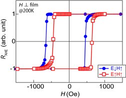
Fig. 2. Perpendicular exchange bias switching induced by an MEFC process for the Al2O3/Pt (25 nm)/Cr2O3 (250 nm)/Pt (1 nm)/Co (1 nm)/Pt (5 nm) all-thin-film system obtained by AHE measurement at 200 K. By applying parallel magnetic and electric fields (Hfr = +10 kOe, Efr = +40 kV/cm), a positive exchange bias state is stabilized (red open squares), whereas by applying antiparallel magnetic and electric fields (Hfr = +10 kOe, Efr = −40 kV/cm), a negative exchange bias state is stabilized (blue solid circles). Results reproduced from Ref. 80 with permission. © 2014 AIP Publishing.
Download figure:
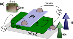
Standard image High-resolution imageAfter the first demonstration of ME manipulation, it was found to be essential to clarify the origin of the larger ME manipulation energy (EH product) in an all-thin-film system. One possibility is the suppression of the magnitude of the ME susceptibility α in the Cr2O3 thin film compared with that in Cr2O3 bulk single crystal. Since the difference in the ME energy ΔF = 2αEH becomes the driving force of the ME manipulation, if α is suppressed, the EH product required for the ME manipulation has to increase. To confirm this assumption, the measurement of α in a Cr2O3 thin film is required. However, the detection of the ME signal in Cr2O3 is not easy since the ME susceptibility α of Cr2O3 is relatively small (in this case, the ME signal is αE as the E field induces the magnetization). Such a difficulty is even more prominent for Cr2O3 thin films because the volume of a Cr2O3 thin film is more than three orders of magnitude smaller than that of a typical Cr2O3 bulk single crystal. Thus, several attempts to measure α values with higher sensitivity have been made so far. In the first measurements of the inverse ME effect by Astrov, the magnetization induced by an AC electric field was measured by surrounding pickup coils.6,7) Later, Kita and co-workers used a superconducting quantum interference device (SQUID) magnetometer to detect the magnetization induced by a DC electric field.10,11) After that, Borisov et al. developed a simple new approach using a conventional SQUID magnetometer; they applied an AC electric field to the sample and detected its magnetic response by using the standard AC susceptibility measurement procedure.13) By using Borisov's approach, the first measurement of α in an Al2O3/Pt (25 nm)/Cr2O3 (500 nm)/Pt (25 nm) thin-film system was carried out.90) Soon after, Al-Mahdawi et al. developed a modified α-measurement setup using a conventional SQUID magnetometer and external lock-in amplifiers; they succeeded in measuring α for similar samples.91) The scheme of the sample setup and the temperature dependence of α measured by Al-Mahdawi et al. are shown in Fig. 3. The temperature profiles of α in the Cr2O3 thin film measured by Borisov et al. and Al-Mahdawi et al.90,91) are similar to that in the Cr2O3 bulk single crystal,6–13) except for a small lowering of TN and the relevant temperature in the Cr2O3 thin film. The most important finding is the almost identical peak value of α in both the Cr2O3 thin film (between 3.4 and 4.6 ps/m90,91)) and the Cr2O3 bulk single crystal (between 3.8 and 5.1 ps/m10–13)). These results clarified that, apart from the suppression of α, other dominant factors contribute to increasing the EH product in the Cr2O3 thin-film system.
Download figure:
Standard image High-resolution image
Fig. 3. (a) Scheme of an ME coefficient measurement setup. (b) Temperature dependence of the ME coefficient α of a 500-nm-thick Cr2O3 thin film deposited by reactive sputtering. The simultaneously measured leakage current is also shown (brown line) and used for background correction. The open square and the solid triangle indicate uncorrected and corrected data, respectively. Results reproduced from Ref. 91 with permission. © 2017 IOP publishing.
Download figure:
Standard image High-resolution imageFigure 4 summarizes the threshold ME manipulation energies (threshold EH products EthHfr) reported for both a Cr2O3 bulk single crystal and a Cr2O3 thin film in an MEFC process as a function of JK/tAF (noted as "Typical system").23,64,80,84) Here, JK = HexMstFM is the unidirectional anisotropy energy induced by exchange bias; tAF, Hex, Ms, and tFM are the Cr2O3 thickness, exchange bias magnitude, saturation magnetization of Co, and Co thickness, respectively. The JK data in Fig. 4 were mainly measured at 250 K, whereas the data from Ref. 64 were measured at 265 K. As can be seen from Fig. 4, the EthHfr and JK/tAF values are linearly correlated, as indicated by the black dashed line that closely fits the data. These results allow us to estimate the following simplified free energy model for Cr2O3 under Hfr and Efr in an MEFC process:32,83)

Here, WME and WEX denote the ME term and exchange bias term of the free energy, respectively. Jint is the interface exchange coupling energy, which is strongly correlated with JK. Because it is a field cooling process, we neglect the antiferromagnetic anisotropy term KAF sin2 θ. The threshold condition for the switching at around TN of Cr2O3 is

Since α is almost constant regardless of its form (bulk or thin film), if we assume a strong positive correlation between Jint and JK, Eq. (3) indicates a linear relation between EthHfr and JK/tAF, which well agrees with the trend observed in Fig. 4. The relation in Eq. (3) can be qualitatively interpreted as follows: when we apply a positive Hfr, the neighbor ferromagnetic domains align along the magnetic field direction (positive direction) and the Cr2O3 antiferromagnetic domains receive induced unidirectional anisotropy from the ferromagnetic domains through the exchange bias. This is the same as the usual magnetic field cooling process in exchange bias systems. However, since Cr2O3 is an ME material, Cr2O3 antiferromagnetic domains can be controlled to the desired direction by applying both magnetic and electric fields. To switch the Cr2O3 antiferromagnetic domains against the unidirectional anisotropy induced by the exchange bias, an EH product greater than Jint/αtAF is required. Given that the ME energy depends on the sample volume, whereas the exchange bias energy depends on the sample interface, a decrease in the Cr2O3 thickness will increase the threshold EH product. This should explain the larger ME manipulation energy for Cr2O3 all-thin-film systems. The threshold EH product is also proportional to Jint, i.e., the threshold EH product increases as the Hex magnitude increases. Thus, referring to Fig. 2, we could easily realize the ME manipulation of exchange bias by reducing the Hex magnitude by using a Pt spacer. However, the negative correlation between the ME manipulation energy and the Cr2O3 thickness is a critical problem, especially toward practical applications, where Cr2O3 films should be made as thin as possible. Nevertheless, the electric field required for ME switching increases inversely proportionally to the Cr2O3 thickness, and finally it exceeds the maximum breakdown voltage of the Cr2O3 thin film. That means we cannot achieve the ME manipulation of exchange bias for even thinner Cr2O3 films.

Fig. 4. Relationship between threshold EH product EthHfr and JK/tAF in MEFC processes. The "Typical system" plots indicate the results of Cr2O3 bulk and thin-film systems without Cr2O3 magnetization; the dashed line indicates the linear correlation found between EthHfr and JK/tAF. The "System with MCr2O3" plots indicate the minimum EthHfr of Cr2O3 thin-film systems with Cr2O3 magnetization; here, EthHfr is almost independent of JK/tAF.
Download figure:
Standard image High-resolution imageThis problem occurs as long as we use an exchange bias for readout, which imposes a limit on the Cr2O3 thickness. Moreover, this issue occurs not only for MEFC manipulation but also for isothermal manipulation. Recently, a possible way to overcome the problem was found; the unexpected finite magnetization in Cr2O3 plays an important role in this sense. Although Cr2O3 is an AFM, occasionally finite magnetization has been observed in Cr2O3 films.32,83,90,92–101) The origin of such finite magnetization is still under debate; it has been attributed to piezomagnetism,92) boundary magnetization,90,93–97,102) defect-mediated magnetization,98–101) and so forth. In an exchange bias system, the magnetization from an antiferromagnetic layer sometimes evokes a curious positive exchange bias phenomenon,59) in which both the sign and magnitude of the exchange bias vary by changing the magnitude of the applied magnetic field Hfr during the magnetic field cooling process. Figure 5 shows an example of the positive exchange bias phenomenon observed in an Al2O3/Pt (25 nm)/Cr2O3 (250 nm)/Pt (tPt)/Co (1 nm)/Pt (5 nm) structure. Here, the exchange bias measured at 100 K is plotted as a function of Hfr; as can be seen, as Hfr increases, the exchange bias changes its sign from negative to positive. This phenomenon is explained by the competition between the exchange bias energy and the Zeeman energy of the Cr2O3 magnetization. With increasing Hfr, the magnitude of the Zeeman energy increases, whereas the exchange bias energy remains constant. As a consequence, at a certain Hfr, the Zeeman energy exceeds the exchange bias energy and the positive exchange bias state is stabilized. The results were well reproduced by an equation that takes into account both the free energy of the system and the thermal fluctuation effect, as shown in Fig. 5. A crucial finding is that the exchange bias energy and the Zeeman energy are fully compensated at the Hfr value at which the exchange bias becomes zero (x-intercept in Fig. 5). This idea can be utilized to reduce the ME manipulation energy in an MEFC process. As mentioned above, the ME manipulation energy strongly depends on the exchange bias energy; thus, if we can minimize the influence of the exchange bias energy by compensating the Zeeman energy, the ME manipulation will become significantly easier to achieve. Such an idea based on low-energy manipulation has been proposed by Al-Mahdawi et al.32) In a system with a finite Cr2O3 magnetization (MCr2O3), if we add the Zeeman term of MCr2O3 (WZM), the free-energy formula becomes
and the threshold condition of the switching at around TN of Cr2O3 is
or

Equation (5) indicates that if a calibrated magnetic field Hfr = Jint/MCr2O3tAF is applied, the exchange bias energy is fully compensated by the Zeeman energy of MCr2O3, and low-energy ME manipulation of the exchange bias becomes possible. This idea was experimentally demonstrated by using an Al2O3/Pt (25 nm)/Cr2O3 (1000 nm)/Pt (tPt)/Co (1 nm)/Pt (5 nm) system.83) For the demonstration, an accidentally obtained finite magnetization of Cr2O3 was used, the same as that also used for the observation of the positive exchange bias phenomenon.59) At that stage, we did not know the exact origin of MCr2O3 and we could not control its magnitude. However, we observed such magnetization in a reproducible fashion. Given the limitations to the applicable magnetic field, to obtain a fully compensated state (Hfr = Jint/MCr2O3tAF) within an applicable magnetic field, we needed to design Jint and tAF. In the demonstration, we used a 1000-nm-thick Cr2O3 film to obtain a fully compensated state with a relatively small magnetic field. The effective magnitude of Jint was controlled by changing the thickness of the Pt spacer layer. To study the relation of the compensation, an Eth vs 1/Hfr plot of the ME manipulation energy was used. In this plot, the y-intercept and slope are related to MCr2O3/α and Jint/αtAF, respectively, as we can estimate from Eq. (5). Figure 6 shows Eth as a function of 1/Hfr in the context of MEFC manipulation.83) The x-intercept represents the fully compensated point (Hfr = Jint/MCr2O3tAF). The fitting lines of all samples are characterized by almost the same negative y-intercepts, corresponding to the similar MCr2O3 values of the samples. The slopes of the fitting lines increase as the Pt thickness decreases, i.e., as the Hex magnitude increases. Due to the negative y-intercepts owing to the existence of finite MCr2O3 values, all samples exhibit finite x-intercepts, thus indicating that the low-energy manipulation of the exchange bias is possible. The minimized threshold EH product obtained from Fig. 6 is also plotted in Fig. 4 by red solid diamonds (labeled as "System with MCr2O3"). While the "Typical system" data show a linear increase in the threshold EH product with increasing JK/tAF, the "System with MCr2O3" data exhibit an almost constant trend. Even for a 1000-nm-thick Cr2O3 system with an untunable small MCr2O3, we achieved a reduction of approximately two orders of magnitude for the threshold EH product. However, significant benefits will be obtained when the Cr2O3 sample becomes much thinner. Referring to Fig. 4, for JK/tAF ∼ 105 emu/cm3 (corresponding to tAF < 10 nm), the EH product required to overcome the exchange bias energy becomes ∼105 kOe kV/cm. Thus, even if Hfr of 10 kOe is applied, Eth becomes as large as 10 MV/cm, which is higher than the applicable electric field, and ME manipulation can no longer be achieved. If a larger Cr2O3 magnetization is obtained, a reduction of several orders of magnitude for the threshold EH product will be possible, and the limitation of the Cr2O3 thickness can be overcome. Further elucidation of the origin of MCr2O3 and also ways to control it are issues under study.
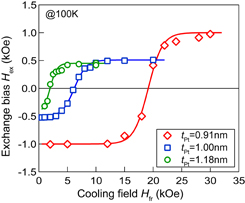
Fig. 5. Example of positive exchange bias phenomenon observed in Al2O3/Pt (25 nm)/Cr2O3 (250 nm)/Pt (tPt)/Co (1 nm)/Pt (5 nm) structure measured at 100 K. With increasing Hfr, the exchange bias polarity changes from negative to positive. Fitted lines are also shown. Results reproduced from Ref. 59 with permission. © 2014 AIP Publishing.
Download figure:
Standard image High-resolution image
Fig. 6. Eth vs 1/Hfr plot for MEFC manipulation of the exchange bias in an Al2O3/Pt (25 nm)/Cr2O3 (1000 nm)/Pt (tPt)/Co (1 nm)/Pt (5 nm) system with Cr2O3 magnetization. x-intercepts indicate points where the exchange bias energy and the Zeeman energy of Cr2O3 magnetization are fully compensated. At these points, low-energy MEFC manipulation is possible. Results reproduced from Ref. 83 with permission. © 2017 The Japan Society of Applied Physics.
Download figure:
Standard image High-resolution image2.2. Isothermal manipulation
ME manipulation for Cr2O3/Co all-thin-film systems in an isothermal process was realized by two groups in 2015,84,85) soon after the demonstration in an MEFC process. Since the necessity of a much higher voltage in an isothermal process than that in an MEFC process was assumed, significant effort was made to develop higher-breakdown-voltage samples. As a result, breakdown voltages of MV/cm order have been achieved, thus allowing the realization of isothermal ME manipulation in Cr2O3 all-thin-film systems. Figure 7 summarizes the isothermal manipulation of the exchange bias in an Al2O3/Pt (25 nm)/Cr2O3 (500 nm)/Cr (0.25 nm)/Co (1 nm)/Pt (5 nm) system.84) As can be seen, the switching of the exchange bias polarity by simply changing the isothermal electric field Eiso while maintaining the isothermal magnetic field Hiso was clearly demonstrated [Figs. 7(a) and 7(b)]. In these studies, a small coercive field of Co was realized by using a Cr spacer layer while maintaining its perpendicular magnetic anisotropy. Such a smaller coercive field (<50 Oe) than the exchange bias magnitude (∼100 Oe) enables Co magnetization switching at zero magnetic field, in addition to the exchange bias polarity reversal. In this study, repeated operations of exchange bias/Co magnetization switching were also demonstrated [Figs. 7(c) and 7(d)].

Fig. 7. Demonstration of isothermal ME manipulation of both perpendicular exchange bias and Co magnetization for Al2O3/Pt (25 nm)/Cr2O3 (500 nm)/Cr (0.25 nm)/Co (1 nm)/Pt (5 nm) all-thin-film system at 280 K. (a) Perpendicular exchange biased hysteresis loop obtained after initial magnetic field cooling process with Hfr = −6 kOe (black open circles) and after isothermal ME manipulation with Eiso = −1600 kV/cm and Hiso = +6 kOe (green open circles). (b) Perpendicular exchange biased hysteresis loop obtained after isothermal ME manipulation with Eiso = −1600 kV/cm and Hiso = +6 kOe (green open circles) and after isothermal ME manipulation with Eiso = +2000 kV/cm and Hiso = +6 kOe (red open circles). (c) Isothermal perpendicular exchange bias switching plotted against number of repeated manipulation cycles. (d) Isothermal Co magnetization switching plotted against number of repeated manipulation cycles. Results reproduced from Ref. 84 with permission. © 2015 AIP Publishing.
Download figure:
Standard image High-resolution imageME manipulation experiments based on the MEFC process are crucial to understand the effect of the exchange bias energy on ME manipulation but are not suitable for practical applications. Although the possibility of heat-assisted operation using an MEFC process still remains, isothermal manipulation would be a more realistic candidate for spintronic applications. Thus, the understanding of isothermal ME manipulation is essential. However, it is not easy to investigate the manipulation properties in an isothermal process, since they require much higher EH product values for the switching than those in an MEFC process. Recently, some updates concerning the isothermal manipulation energy were reported. In order to understand the switching mechanism,86,87) the magnetic field dependence of the threshold EH product was measured by using a large magnetic field (Hiso > 40 kOe). The results indicated that the nucleation and growth of the antiferromagnetic domains occur in the isothermal process. However, a full understanding of isothermal ME manipulation is yet to be achieved and further investigation is required. The investigation will be accelerated if the isothermal manipulation energy can be reduced.
Another important aspect of isothermal ME manipulation is the elucidation of the switching dynamics in the Cr2O3/Co exchange bias system. Since Cr2O3 is an AFM, ultimately, operations on the order of ps are expected,103–106) whereas a slightly worse operation speed is expected to characterize in Cr2O3/FM exchange bias systems. Through pulse voltage application experiments, the dynamics of an Al2O3/Pt (20 nm)/Cr2O3 (150 nm)/Au (0.5 nm)/Co (0.4 nm)/Pt (1.5 nm) system was investigated by AHE measurement with a Hall bar of 2 × 2 µm2 cross point.86) The switching time in isothermal switching depends on the applied EH product: when a sufficiently large EH product is applied, switching time periods shorter than 10 ns are obtained, whereas when the EH product is close to the threshold value, the switching time is on the order of 100 ns. These results suggest that the switching nature is governed by domain wall motion. The estimated minimal domain wall mobility was 2 × 10⁻³ m s−1 Oe−1 at 540 kV/cm. However, the domain wall mobility has room for further enhancement, as demonstrated by Belashchenko et al.107) in the prediction of a two-orders-of-magnitude higher maximum mobility for Cr2O3. In addition, the switching speed should increase with decreasing element size. In the future, operations with a time period below sub-ns order will possibly be realized, comparable with SOT-type108) or voltage-torque-type36,37) ultrahigh-speed-operation MRAMs, or even faster.
Another notable topic is FM-free operation. As mentioned above, while the exchange bias has a strong merit in terms of readout, it interrupts the ME manipulation of Cr2O3. In addition, it can partially degrade the excellent properties of an antiferromagnetic material, such as the THz resonance frequency and no stray field. Although difficulties in the readout have to be overcome, FM-free structures offer the possibility of futuristic ultrahigh-performance spintronic device applications. As another kind of readout technique, the spin hall magnetoresistance of Cr2O3 has recently been measured.109) Moreover, the interface polarization of overlayer paramagnets, such as Pt and Pd on Cr2O3, was found, which was detected by X-ray magnetic circular dichroism (XMCD)110) and AHE measurement.111) Kosub et al. demonstrated purely antiferromagnetic ME random access memory operation in a Pt (20 nm)/Cr2O3 (200 nm)/Pt (2.5 nm) structure by AHE detection of the induced interface polarization.101) Of course, some issues still remain, such as a relatively large footprint owing to the need for AHE detection and a small AHE signal magnitude; however, this is an attractive technique for future applications.
Since the first demonstration of ME manipulation in a Cr2O3 all-thin-film system in 2014,80) significant progress has been made in the understanding of its mechanism and many beneficial properties have been elucidated. Recently, research studies motivated by device applications have also become active. For example, some studies related to the local writing of exchange bias have been exploited65,71) for storage application;32) further applications of this field, including the use of the spin Seebeck effect,112) spin transport,113) and graphene transistors,114–117) were also reported. Further progress is expected for electrically controllable AFM Cr2O3 thin films.
3. Toward room temperature operation
In this section, we review the attempts made to enhance the operating temperature. For device applications, the enhancement of the operating temperature is a high-priority task. To achieve a high operating temperature, both TN and the perpendicular magnetic anisotropy have to be enhanced. In the research performed along this direction, theoretical calculation/predictions play an important role for experimental demonstrations. First, we will summarize the current situation and the remaining issues toward the enhancement of TN, then we will describe the enhancement of the perpendicular magnetic anisotropy in a Cr2O3 thin-film system.
3.1. Néel temperature
The Néel temperature of Cr2O3 (TN ∼ 307 K), which is relatively high among the well-characterized ME materials, does not provide enough flexibility for practical applications. The insufficient TN has been recognized as a paramount issue and several solutions have been proposed to overcome this limitation.
The first one concerns impurity substitution. Since the magnetic interaction in Cr2O3 is dominated by the Cr–Cr direct exchange interaction, any change in the Cr–Cr bond length strongly affects the effective exchange field. In addition, the impurity states introduced by doping can further affect the exchange coupling. In this regard, Mu et al., through electronic structure calculations, investigated the doping effect of several anions (V, Ti, Mn, Fe, Co, and Ni) and cations (N and B) on the effective exchange field of Cr2O3.118) Although transition-metal impurities reduce TN of Cr2O3, Mu et al. found that B doping can enhance TN while retaining a large excitation gap, i.e., retaining its insulating properties. This is because the B doping introduces hybrid impurity states, which strongly enhance the exchange energies for the Cr neighbor ions. Mu et al. predicted an increase in the TN of Cr2O3 by approximately 10% per 1% of O sites substituted by B. Later, Street et al.94) experimentally enhanced TN of Cr2O3 up to 400 K by B doping. They estimated the change in TN from the temperature dependence of the measured remnant boundary magnetization. Despite the experimental demonstration of TN ∼ 400 K, several challenges still remain, including the difficulty of substituting an anion O site with B. Given that B easily becomes a cation, such as B2O3, a specific technique is required to fabricate B-doped Cr2O3. In their report, Street et al. adopted the pulsed laser deposition method, letting the Cr2O3 target be immersed in a B10H14 background gaseous atmosphere. In contrast, high-quality Cr2O3 films have recently been fabricated by a reactive sputtering method. The development of a fabrication technique for high-quality B-doped Cr2O3 by sputtering is one challenge. Another challenge is the stabilization of B into the Cr2O3 matrix. Since B has an exceptionally small atomic radius, it easily diffuses after repeated heat treatments. However, given the fact that B doping is the most promising solution for TN enhancement, overcoming all these issues will be the key to practical applications.
The second approach is strain engineering. As previously specified, since the magnetic interaction in Cr2O3 is dominated by the Cr–Cr direct exchange interaction rather than the super-exchange interaction, changes in the bond length due to lattice strains strongly affect TN. Strain engineering has been adopted for bulk Cr2O3 systems119–123) but not for Cr2O3 thin films. Kota et al. investigated the effect of an isovolumetric elastic strain on TN by first-principles calculations and Monte Carlo simulations.123–125) The variation of the calculated TN with the c/a ratio is shown in Fig. 8 (red solid circles). It was found that TN is enhanced by a tensile strain and decreased by a compressive strain along the c-axis. The effect of the lattice strain is relatively large; in particular, more than 20% of the TN enhancement was estimated to be due to 5% tensile strain in the crystal lattice. Such strain-induced TN control has been partly demonstrated for Cr2O3 thin-film systems,60,66) where several different buffer layers were used to control the lattice strain. TN was identified in a low-magnetic-field M–T measurement using the Cr2O3/Ru/Co exchange bias system, where the magnetic anisotropy of Co was well tuned by using a Ru spacer layer for the detection of TN.66) In Fig. 8, the experimentally obtained TN of a buffered Cr2O3 film is plotted against the c/a ratio60,66) in addition to the calculated TN variation.124) As can be seen, the calculated TN variation is well reproduced by experiments, thus confirming the correctness of the calculated data. Unfortunately, at present, experimental results have only been obtained for compressive strain regions, thus showing a decrease in TN. To enhance TN, it is necessary to develop suitable buffer layers.

Fig. 8. Calculated TN variations of Cr2O3 with c/a ratio under an isovolumetric elastic strain in Ref. 124 (red solid circles, left axis) and experimentally obtained TN of Cr2O3 in Al2O3/buffer layer/Cr2O3 (20 nm)/Ru (1.25 nm)/Co (1 nm)/Pt (5 nm) structure with Pt, Al2O3, and α-Fe2O3 buffer layers in Ref. 60 (black open diamonds, right axis), and those with Pt, Ir-doped α-Fe2O3, and α-Fe2O3 buffer layers in Ref. 66 (blue open circles, right axis).
Download figure:
Standard image High-resolution imageThe third approach is to exploit the enhancement of spin correlations by using the AFM/AFM proximity effect. The idea is that when a thin Cr2O3 film is placed next to a high-TN AFM, even at T > TN of Cr2O3, retention of the antiferromagnetic correlation of Cr2O3 near the interface is expected because of the antiferromagnetic correlation with the neighbor high-TN AFM. This behavior has been demonstrated for thick NiO (TN ∼ 523 K) and thin CoO (TN ∼ 293 K) bilayer systems.126,127) Suggestive results have also been obtained for nanocomposite structures, including Cr2O3 and α-Fe2O3.128) Kota et al. calculated the spin correlation enhancement effect in the α-Fe2O3/Cr2O3 structure.129) In their study, α-Fe2O3 was selected for a high-TN AFM as it has a high TN (∼ 950 K) and the same corundum-type crystal structure as Cr2O3. The calculation results indicate that the spin correlation of Cr2O3 near the interface is sustained even at 1.5 times TN of Cr2O3 (∼ 450 K) when an oxygen-divided interface is realized at the α-Fe2O3/Cr2O3 interface. On the basis of these calculation results, research on the α-Fe2O3/Cr2O3 structure has been going on. In order to obtain α-Fe2O3 with a perpendicular spin configuration, the enhancement of the Morin transition temperature of α-Fe2O3 by Ir doping was demonstrated.130–133) The spin correlation length of Cr2O3 was experimentally estimated from a finite-size scaling effect of TN.66) However, the TN enhancement due to the spin correlation enhancement in an Ir-doped α-Fe2O3/Cr2O3 system has not yet been demonstrated, probably because of the interfacial mixing or metal-split-type interface at the Ir-doped α-Fe2O3/Cr2O3 interface. Thus, to achieve such a demonstration, an advanced interface control technique has to be developed.
3.2. Magnetic anisotropy
To achieve a sufficiently high operating temperature, not only TN but also the perpendicular magnetic anisotropy has to be enhanced. Essentially, the magnetic anisotropy has the role of maintaining the thermal stability. In addition, in exchange bias systems, the magnetic anisotropy is related to the blocking temperature of the exchange bias, TB, as has been discussed on the basis of the MB model.45,78,79) When the value of the KAFtAF product is not sufficient, TB significantly lower than TN has been observed in the Cr2O3/Co exchange bias system. The domain wall width is also related to the magnetic anisotropy.134) Thus, a high perpendicular magnetic anisotropy is required for devices characterized by domain-wall-related phenomena. For these reasons, effort has been made to enhance the perpendicular magnetic anisotropy. In this section, we describe the enhancement of the magnetic anisotropy by using lattice strain and doping. One of the most basic difficulties in this sense is the lack of an easy way to evaluate the magnetic anisotropy of an AFM. Typically, magnetic anisotropies of an AFM have been evaluated by antiferromagnetic resonance (AFMR) measurements.135) However, it is difficult to adopt such a technique of measurement for antiferromagnetic thin films. In this section, we will qualitatively discuss the magnetic anisotropy of Cr2O3 films based on the relation between the magnetic anisotropy and TB, where TB increases as the magnetic anisotropy increases.
As shown in the previous section, lattice strains affect TN through a change in the exchange interactions. In addition, lattice strains distort CrO6 octahedra, thus changing the single-ion anisotropy (or magnetocrystalline anisotropy) through the modulation of the crystal field. Kota and Imamura estimated the strain dependence of single-ion anisotropy by first-principles calculations and clarified that the single-ion anisotropy increases monotonically with a.134) Another notable finding is the extremely small single-ion anisotropy of Cr2O3 in the equilibrium state. A possible one-order-of-magnitude enhancement of single-ion anisotropy by a small lattice strain (∼1%) was indicated. Experimental results consistent with the calculated lattice strain dependence of the magnetic anisotropy trend were obtained for Cr2O3 (20 nm)/Ru (1.25 nm)/Co (1 nm) exchange bias systems with different buffer layers.67) The buffer layer was changed from Pt to α-Fe2O3, which increases a for the Cr2O3 layer, thus resulting in a large enhancement of TB. A rough/semiquantitative estimation based on the MB model suggests an enhancement of the magnetic anisotropy of about fourfold by changing the buffer layer. These results confirm the effectiveness of the lattice strain for enhancing the magnetic anisotropy. It is important to note that, while increasing the lattice parameter a yields an increase in the single-ion anisotropy, it simultaneously causes a slight decrease in TN. For example, when the magnetic anisotropy was enhanced fourfold, a decrease in TN of 25 K (from 294 to 269 K) was observed. We have to take into account these contradictory properties when we utilize the lattice strain effect for operating-temperature engineering.
There have been some reports of the enhancement of the magnetic anisotropy of Cr2O3 by doping for a Cr2O3 bulk system136,137) but not for a Cr2O3 thin-film system. This mainly reflects the difficulty in the evaluation of such enhancement in Cr2O3 thin-film systems. We fabricated Al-doped Cr2O3/Co exchange-biased thin films and evaluated the dopant concentration dependence of the magnetic anisotropy through the change in TB.72) TB increases as the Al content increases, thus indicating a monotonic increase in the magnetic anisotropy. The increment of TB is much larger than that obtained by lattice strain effects, thus suggesting the effectiveness of Al doping in enhancing magnetic anisotropy, while it is difficult to evaluate the increment quantitatively. Although some theoretical considerations were presented, the mechanism has not yet been completely clarified. For example, the change in the magnetic anisotropy was discussed in terms of the change in lattice parameters; such changes, as specified above, can modulate the magnetic anisotropy by more than one order of magnitude. Figure 9 shows calculated single-ion anisotropy variations when both lattice parameters a and c are changed.72) The experimental values of the lattice parameters of Pt-buffered undoped Cr2O3, Pt-buffered Al-doped Cr2O3, and α-Fe2O3-buffered undoped Cr2O3 thin films are plotted in the same figure. As can be seen from Fig. 9, in Al-doped Cr2O3, both a and c decrease almost isotropically, reflecting the smaller ionic radius of Al3+ than that of Cr3+. As the Al content increases, the decrease becomes larger. However, Fig. 9 indicates that single-ion anisotropy is not significantly changed by isotropic deformation. This is in contrast to the expected large change in the single-ion anisotropy for α-Fe2O3-buffered undoped Cr2O3 (black open inverted triangle in Fig. 9), where c is increased and a is decreased. In addition, the experimentally observed enhancement of the magnetic anisotropy due to Al doping cannot be explained from changes in the electronic structure. These results indicate that, in addition to conventional lattice strains, there is a mechanism to enhance the magnetic anisotropy of Cr2O3, whose origin, however, is not yet clarified. To summarize, the parallel use of lattice strain and doping methods is a promising way to obtain a sufficiently high perpendicular magnetic anisotropy. Since, at present, the development of high-magnetic-anisotropy antiferromagnetic materials is mainly limited by the lack of evaluation techniques, progress in this area is crucial.

Fig. 9. Calculated lattice parameter a and c dependences of single-ion (magnetocrystalline) anisotropy of Cr2O3. The positive (negative) values indicate perpendicular (in-plane) magnetic anisotropy. The experimental a and c values of undoped (black open circle), Al 3.7%-doped (red open square), and Al-doped (blue open diamonds) Cr2O3 samples are plotted; a and c values of Pt-buffered (black open triangle) and α-Fe2O3-buffered (black open inverted triangle) 20-nm-thick Cr2O3 samples are also plotted. Results reproduced from Ref. 72 with permission. © 2017 The Japan Society of Applied Physics.
Download figure:
Standard image High-resolution image
4. Conclusions
In this report, we reviewed the progress made thus far in the magnetoelectric manipulation and operating temperature in Cr2O3 thin films. The understanding of the mechanism of magnetoelectric manipulation has advanced and a lowering of the manipulation energy has been partly demonstrated. In the future, the investigation trend will concern thinner Cr2O3 regions. For the operating temperature, it has been demonstrated that a sufficiently high TN (> 350 K) and perpendicular magnetic anisotropy are no longer impossible targets. Both these goals will be achieved in the future by stable forms, as the remaining issues have been summarized. Initially, the investigation of the magnetoelectric manipulation of Cr2O3 was aimed at nonvolatile memory applications. However, further applications of this field have recently been proposed. The electrically controllable antiferromagnets are expected to receive increasing attention in the future development of spintronics as more promising materials than conventional ferromagnetic materials. We believe that Cr2O3, the first-discovered magnetoelectric material, will lead the era of "antiferromagnetic spintronics" through continuous material development.
Acknowledgments
The authors would like to thank C. Binek, P. Borisov, H. Imamura, Y. Kota, Y. Kitaoka, K. Mibu, T. Mitsui, Y. Shiratsuchi, T. Kimura, E. Kita, H. Yanagihara, T. Shibata, S. Yonemura, Y. Shiokawa, S. P. Pati, M. Al-Mahdawi, S. Ye, N. Shimomura, T. Ashida, Y. Sato, and M. Oida for fruitful discussions and technical support. This work was partly funded by the Advanced Low Carbon Technology Research and Development Program (ALCA) of the Japan Science and Technology Agency (JST), the ImPACT Program of Council for Science, Technology and Innovation (Cabinet Office, Japan Government), the Murata Science Foundation, a Grant-in-Aid for Japan Society for the Promotion of Science (JSPS) Fellows, and JSPS KAKENHI Grant Number 16H05975.