

Abstract
In this paper, the current–voltage (I–V) characteristics of a 600-V-class normally off GaN gate injection transistor (GIT) from 25 to 200 °C are analyzed, and it is revealed that the drain current of the GIT increases during high-temperature operation. It is found that the maximum drain current (Idmax) of the GIT is 86% higher than that of a conventional 600-V-class normally off GaN metal insulator semiconductor hetero-FET (MIS-HFET) at 150 °C, whereas the GIT obtains 56% Idmax even at 200 °C. Moreover, the mechanism of the drain current increase of the GIT is clarified by examining the relationship between the temperature dependence of the I–V characteristics of the GIT and the gate hole injection effect determined from the shift of the second transconductance (gm) peak of the gm–Vg characteristic. From the above, the GIT is a promising device with enough drivability for future power switching applications even under high-temperature conditions.
Export citation and abstract BibTeX RIS
1. Introduction
Wide-bandgap semiconductors are suitable for high-breakdown-voltage and high-temperature-resistance devices. Wide-bandgap semiconductors are expected for future power switching applications and have been intensively researched recently.1–11) GaN power devices are among the intensively investigated wide-bandgap semiconductors because of their high drain current and high switching speed compared with Si power devices.12–16) GaN high electron mobility transistors (HEMTs) are widely researched because of their high electron density owing to the two-dimensional electron gas (2DEG) that is formed in the AlGaN/GaN boundary surface.17–22) However, GaN HEMTs are normally on devices and they have a problem in safety operation for power switching applications. Thus, various types of normally off GaN power devices are proposed.14–16,23,24) Metal–insulator–semiconductor hetero-FETs (MIS-HFETs) are normally off GaN power devices. MIS-HFETs, whose structure is shown in Fig. 1, have an insulator formed over the AlGaN/GaN heterostructure and can control high drain current with low gate current.23,25,26) MIS-HFETs also have issues regarding the current collapse phenomenon and drain current degradation at high temperatures. The devices with large current degradation and without enough drivability at high temperatures cannot guarantee the operation of devices at high temperatures. In order to compensate for their degraded current capacity, more devices are required, which will lead to rising cost of their products. Therefore, normally off devices that have little drain current degradation and have high drivability at high temperatures are needed. Gate injection transistors (GITs) are another attractive normally off GaN power devices because they achieve current collapse-free operation by hole injection from the p-AlGaN gate.24,27,28) In GITs, the temperature dependence of threshold voltage and switching time was reported in Ref. 29. It has also reported that the hole injection of GITs can be examined by the second peak of the gm–Vg characteristic.30) However, current–voltage (I–V) characteristics such as the drivability and physical operation mechanism of GITs under high-temperature conditions have not been clarified yet.
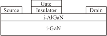
Fig. 1. Structure of the conventional MIS-HFET.
Download figure:
Standard image High-resolution imageIn this work, we analyzed the Id–Vd/Id–Vg characteristics of a 600-V-class GaN GIT from a room temperature of 25 °C to a high temperature of 150 °C, and the maximum drain current of the GIT is compared with that of a conventional 600-V-class MIS-HFET.31) In addition, we measured the Id–Vd characteristics of the GIT at high temperatures up to 200 °C and extracted the maximum drain current to confirm its current degradation at high temperatures up to 200 °C. Moreover, we clarified the mechanism of the drain current enhancement of the GIT determined from the shift of the second transconductance (gm) peak of the gm–Vg characteristic under high-temperature conditions.
2. Experimental methods
Figure 2 shows the measured 600-V-class GIT structure and its geometry. The GIT has a p-AlGaN gate formed over the AlGaN/GaN heterostructure.24) The structure that is related to the size of the GIT is similar to that of the MIS-HFET. The length from the gate to the drain (Lgd), gate length (Lg), and length from the source to the gate (Lsg) are 10, 2, and 1.5 µm, respectively. The gate width of the GIT is 100 µm. The measurement setup is shown in Fig. 3. Id–Vd and Id–Vg characteristics are measured with the power device analyzer B1505A. Temperature is adjusted by the temperature controller from room temperature (25 °C) to a high temperature (200 °C) when these characteristics are measured. The drain voltage is applied from 0 to 10 V with the gate voltage from 0 to 6 V by the power device analyzer. These characteristics are measured by the four-terminal and pulse sweep measurement methods. The pulse sweep measurement method is used to prevent the underestimation of the drain current due to self-heating of the GIT and to obtain its temperature dependence with the minimum influence of the self-heating. Then, the temperature dependence of the maximum drain current (Idmax) of the GIT and MIS-HFET is extracted from the Id–Vd characteristic at Vg of 6 V. The temperature dependence of the Idmax of the 600-V-class GIT is compared with that of the conventional commercial 600-V-class MIS-HFET GB66502B.25)

Fig. 2. Structure and geometry of the measured GIT.
Download figure:
Standard image High-resolution image
Fig. 3. Measurement setup.
Download figure:
Standard image High-resolution image3. Results and discussion
Figure 4 shows the measured Id–Vd characteristics of the GIT at 25 and 150 °C. The GIT showed 27 mA Id with Vg of 6 V at 25 °C and 18 mA Id with Vg of 6 V at 150 °C. The Idmax is extracted from the measured Id–Vd characteristics at Vg of 6 V. Then, it is normalized by the value at 25 °C. The temperature dependence of normalized Idmax is compared with that of the conventional MIS-HFET as shown in Fig. 5. The Idmax from 25 to 150 °C of the conventional MIS-HFET is described in Ref. 25. The normalized Idmax of the 600-V-class GIT at 150 °C is 0.65 and the normalized Idmax of the conventional 600-V-class MIS-HFET at 150 °C is 0.35. The Idmax of the 600-V-class GIT at 150 °C is 86% higher than that of the conventional 600-V-class MIS-HFET. It is revealed that the Idmax degradation of the GIT due to the temperature increase is suppressed compared with that of the conventional MIS-HFET. Moreover, the normalized Idmax of the GIT is 0.56 even at the temperature of 200 °C in Fig. 5. The GIT shows over 52% Idmax at 200 °C while the conventional MIS-HFET shows 52% Idmax at 100 °C. That is, the GIT can drive with Idmax degradation at 200 °C that is smaller than that at 100 °C for the conventional MIS-HFET.

Download figure:
Standard image High-resolution image
Fig. 4. Measured Id–Vd characteristics of the GIT at (a) 25 and (b) 150 °C.
Download figure:
Standard image High-resolution image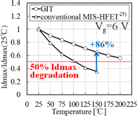
Fig. 5. Temperature characteristic of the normalized maximum drain current Idmax.
Download figure:
Standard image High-resolution imageFigure 6 shows the measured Id–Vg characteristics of the GIT at Vd of 4 V from 25 to 150 °C. The drain current increases with the Vg increase even when the Vg is sufficiently large from 25 to 150 °C, which suggests hole injection occurs. The gm–Vg characteristics of the GIT that are extracted from the measured Id–Vg characteristics are shown in Fig. 7. The second peak occurs between Vg values of 4 and 6 V in the gm–Vg characteristics and the second peak at such high gate voltages is the evidence of hole injection.24,30) The injected holes induce conductivity modulation of the channel, and drain current increases. Thus, the drain current increase suggests the occurrence of hole injection. Moreover, the second peak shifts to lower Vg values with increasing temperature. Therefore, the hole injection occurs at lower Vg values with increasing temperature.
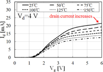
Fig. 6. Measured Id–Vg characteristics of the GIT from 25 to 150 °C.
Download figure:
Standard image High-resolution image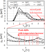
Fig. 7. gm–Vg characteristics of the GIT from 25 to 150 °C.
Download figure:
Standard image High-resolution imageNext, the mechanism model of the drain current enhancement phenomenon is proposed as follows. The operation principle of the hole injection of the GIT is shown in Fig. 8. The holes are injected from p-AlGaN to i-GaN when the gate voltage Vg is over the built-in voltage Vbi. The injected holes gather electrons and the electrons are moved with high mobility by the drain bias compared with the holes that remain around the gate because the electrons have higher mobility than the holes. Conductivity modulation of the channel of the GIT is induced by the injected holes, resulting in the increase in drain current.24) Thus, the hole injection leads to drain current enhancement. Figure 9 shows the band diagram of the GIT from the gate ohmic to i-GaN. Ec, Ef, and Ev are the energy of conduction band, Fermi energy, and the energy of the valence band, respectively. The shifts of the second peak as temperature increases indicate that Vbi decreases with increasing temperature. As Vbi decreases, the potential barrier between p-AlGaN and i-GaN decreases. Then, more holes are injected from p-AlGaN to i-GaN and more electrons are gathered and moved by the drain bias in 2DEG. Therefore, the Idmax of the GIT increases as induced by the injection of more holes from the p-AlGaN of the gate under high-temperature conditions.
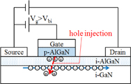
Fig. 8. Operation principle of the hole injection from gate of the GIT.
Download figure:
Standard image High-resolution image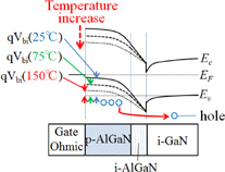
Fig. 9. Band diagram of the GIT at various temperatures.
Download figure:
Standard image High-resolution image
4. Conclusions
The Id–Vd and Id–Vg characteristics of the 600-V-class GIT are measured and the maximum drain current (Idmax) is extracted from Id–Vd characteristics from 25 to 200 °C. It is found that the drain current increases with increasing Vg even when the Vg is sufficiently high from 25 to 150 °C, as determined from Id–Vg characteristics, and the Idmax of the 600-V-class GIT normalized by the value at 25 °C is 86% larger than that of the conventional 600-V-class MIS-HFET. Moreover, the GIT obtains over 52% Idmax at 200 °C while the conventional MIS-HFET obtains 52% Idmax at 100 °C. Then, the gm–Vg characteristic of the GIT is analyzed on the basis of the shift of the second peak. We clarified the mechanism of the drain current enhancement of the GIT by the hole injection under high-temperature conditions with the band diagram at the gate. The temperature rise induces the decrease in Vbi, which leads to more holes being injected and more electrons being gathered by the injected holes. From the above, the GIT is a promising device with enough drivability for future power switching applications even at high temperatures of up to 200 °C.
Acknowledgments
This work was supported by a grant from the New Energy and Industrial Technology Development Organization (NEDO), Japan, under the Strategic Development of Energy Saving Innovative Technology Development Project, "Three-Dimensional Integrated Circuits Technology Based on Vertical BC-MOSFET and Its Advanced Application Exploration" (Research Director, Professor Tetsuo Endoh; Program Manager, Toru Masaoka) of "Accelerated Innovation Research Initiative Turning Top Science and Ideas into High-Impact Values (ACCEL)" under the Japan Science and Technology Agency (JST) Grant Number JPMJAC1301, and the program on Open Innovation Platform with Enterprises, Research Institute and Academia (OPERA) from JST.