

Abstract
Recently, we have developed a two-dimensional (2D) fast-Fourier-transform (FFT) sampling Moiré technique to visually and quantitatively determine the locations of minute defects in a transmission electron microscopy (TEM) image. We applied this technique for defect detection with GaN high electron mobility transistor (HEMT) devices, and successfully and clearly visualized atom-size defects in AlGaN/GaN crystalline structures. The defect density obtained in the AlGaN/GaN structures is ∼1013 counts/cm2. In addition, we have successfully confirmed that the distribution and number of defects closely depend on the process conditions. Thus, this technique is quite useful for a device development. Moreover, the strain fields in an AlGaN/GaN crystal were effectively calculated with nm-scale resolution using this method. We also demonstrated that this sampling Moiré technique is applicable to silicon devices, which have principal directions different from those of AlGaN/GaN crystals. As a result, we believe that the 2D FFT sampling Moiré method has great potential applications to the discovery of new as yet unknown phenomena occurring between the characteristics of a crystalline material and device performance.
Export citation and abstract BibTeX RIS
1. Introduction
It is widely accepted that defect detection techniques are essential for manufacturing semiconductor devices. However, crystalline defects are too minute to detect with high accuracy. Some conventional detection methods are known such as transmission electron microscopy (TEM), cathodeluminescence (CL) analysis, electroluminescence (EL) analysis, electron spin resonance (ESR) analysis, positron annihilation lifetime spectroscopy (PALS),1–5) and X-ray topography. Although cross-sectional TEM observation enables the visual observation of a crystal and also the counting of a portion of defects with relatively high spatial resolution, most of the defects remain invisible or unclear in the obtained TEM images. CL and PL analyses are nondestructive methods that also have high sensitivity for identifying point defects. Nevertheless, the spatial resolutions of CL and EL analyses are at most 100 nm, which is insufficient for identifying the accurate position of each defect. ESR analysis and X-ray topography are suitable for defect estimation of bulk materials or relatively large substrates. Although ESR analysis enables the detection of dangling bonds, whereas X-ray topography enables the identification of slip and/or misfit dislocations, they are not suitable for quantitative or high-spatial-resolution estimation. The PALS method is a relatively new method to detect atomic porosity and nanopores; however, it requires specific and large equipment.
The Moiré phenomenon6) can amplify grating deformation and thereby enable the visualization of defects in a large view field. Since the spatial resolution of TEM in the 1950s and 1960s was not high enough to directly observe crystal grids, Moiré fringes were used for observation of local strains and/or dislocations7–9) at that time. A few groups observed crystalline dislocations10) or strain of semiconductor devices11,12) on the basis of the Moiré phenomenon, and has been proposed in several published papers the combination of the scanning Moiré method with a scanning microscope. Shinoda et al.13) reported that defect formation in Ge islands during the initial growth stages of Ge on Si(111) was characterized on the basis of Moiré patterns taken by TEM. Kondo and Endo14) also reported on the strain analysis of silicon single crystals using the scanning TEM (STEM) Moiré method, where Moiré fringes were generated from TEM scanning lines and silicon crystal grids. In addition, several studies on scanning Moiré methods using laser scanning microscopy (LSM),15) scanning electron microscopy (SEM)16,17) and STEM,18) geometric/overlapping Moiré method,19,20) and the digital Moiré methods21,22) have been carried out to estimate atomic arrays, nanostructures, and butterfly wings. However, the fringe centering technique, which was usually used in the above-mentioned studie, is nonautomatic and has insufficient accuracy. Consequently, the combination of Moiré methods and the temporal phase-shifting technique23,24) was developed to improve accuracy, although this technique can be carried out in only one direction each time and requires a long analysis time. Subsequently, the sampling Moiré method25,26) was proposed for fast and high-accuracy deformation measurements. However, there is no paper on actual defect detection by this method, and a low-pass filter used in the present sampling Moiré method cannot effectively separate the desired gratings in different direction in a two-dimensional (2D) microscope image.
Recently, our group27) has developed a Fourier transform (FT) filtered sampling Moiré technique to detect defects in crystal structures and realized the visualization of minute defects in a large view field with high-accuracy detection, fast automatic processing in any direction, and low cost. As shown in Fig. 1,27) a GaN/AlGaN crystalline structure is separated into several gratings in their principal directions by 2D FT. Using a 2D fast-FT (FFT) filter, the grating images in the x and y directions were obtained. After a sampling pitch was determined, the sampling Moiré fringes were generated and the Moiré phases in the x and y directions were calculated. We successfully detected numerous defects in the GaN/AlGaN crystalline structure with high spatial resolution using Moiré phases (Fig. 2),27) whereas the defects in the original TEM image were too vague to be identified.
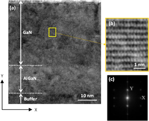
Fig. 1. TEM image and frequency spectrum after 2D FFT. (a) TEM image of AlGaN/GaN structure. (b) Enlarged view of a local area labelled in (a). (c) Frequency spectrum after 2D FET. Reprinted with permission from Ref. 27.
Download figure:
Standard image High-resolution image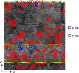
Fig. 2. Defect locations obtained from TEM image in Fig. 1. Reprinted with permission from Ref. 27. © 2017 IOP Publishing.
Download figure:
Standard image High-resolution imageWe also previously reported atom-size defects and strain detection with an AlGaN/GaN HEMT device structure using this 2D FFT sampling Moiré method.28) However, we described only some of the results and our discussion was limited in Ref. 28. Therefore, in this paper, we attempt to demonstrate some new results and discuss further the obtained defects and strain distributions considering the process conditions, especially focusing on the impact of plasma-induced damage on crystalline defects and strain in the AlGaN/GaN heterostructure. Since the plasma-induced damage in GaN and/or AlGaN crystals often deteriorates device performance,29,30) a numerical evaluation of defects in GaN and AlGaN crystals is quite essential. We found that this method enables us to quantitatively estimate defects, and that the defect density is closely related to device performance, as described below.
2. Experimental methods
2.1. Samples
As typical GaN HEMT structures, three blanket AlGaN/GaN stacked films and two patterned AlGaN/GaN structures were prepared for TEM observation and defects/strain detection using the 2D FFT sampling Moiré method. The sample conditions and the structures are summarized in Table I and Fig. 3. In the case of the blanket samples, a stacked structure of AlGaN (30 nm)/GaN/buffer on Si(111) is prepared on 8 in. wafers, and these wafers were cut into small pieces for the following experiment. We adopted the following three conditions for the TEM observation samples: as-epi, after reactive-ion etching (RIE), and RIE followed by a wet treatment. The surface of the AlGaN film was subjected to plasma etching including BCl2/Cl3 gas chemistry at a low power and a low DC bias, realizing a highly controlled etch stop. The detailed conditions were as follows: a BCl3/Cl2 flow rate of 45/155 sccm, a pressure of 20 mTorr, an inductively coupled plasma (ICP) Power of 700 W, and a bias voltage of 131 V. Oxygen ashing followed the RIE process since plasma etching process always accompanies photoresist removal by oxygen ashing in all device fabrication processes. The AlGaN film thickness, which was initially 30 nm before RIE (as-epi), was decreased to 15 nm by plasma etching. In the wet treatment, an oxidizer was added to alkaline followed by acid treatment. This chemical formulation was carefully selected among numerous chemical candidates using a combinatorial method and also confirmed to be effective for removal of the plasma-damaged layer.30,31) All processes including epitaxy growth, plasma etching, and oxygen ashing were performed with commercially available equipment.
Table I. Sample conditions.
| Sample name | Sample structure | Condition |
|---|---|---|
| As-epi | Blanket AlGaN/GaN | Without RIE or wet treatment |
| After RIE | With RIE | |
| After wet treatment | With RIE followed by wet treatment | |
| Before annealing | Recessed AlGaN/GaN | Without thermal annealing after trench RIE |
| After annealing | With thermal annealing after trench RIE |

Fig. 3. Sample structures. (a) As-epi (without RIE or wet treatment). (b) With RIE. (c) With RIE followed by wet treatment. (d) Before annealing. (e) After annealing.
Download figure:
Standard image High-resolution imageAs for the patterned samples assuming a GaN MOSFET structure, the AlGaN/GaN heterostructure grown on a Si substrate was prepared, and afterward recessed by ICP-RIE. Since the recessed surface of the AlGaN/GaN films became rough owing to damage caused by ICP-RIE, one recessed sample was annealed in NH3 ambient to smoothen the rough surface after RIE.32)
All samples for TEM observation were prepared using a focused ion beam (FIB). Subsequently, TEM images with high resolution (e.g., 4000 pixels × 6000 pixels) were obtained using H-9000UHR I (Hitachi). The accelerating voltage was 300 kV.
2.2. Moiré phase analysis
Dislocations and/or defects were visualized and detected by two-step image analysis. The first step is grating extraction by 2D FT where a crystalline structure on a TEM image is separated to gratings in one-dimensional principal directions. The second step is defect visualization using the sampling Moiré method, by which Moiré fringes are generated from the extracted gratings to visualize tiny defects. Although the detailed procedures are reported in Ref. 27, a brief summary is given below. In the first step, gratings in the principal directions are extracted by 2D FFT and 2D inverse FT from an atomic array. For these AlGaN/GaN samples, the X or Y direction agrees with the horizontal or vertical axis, respectively. A diagram of the extracted grating images in the X and Y principal directions is shown in Fig. 4. At this stage, it is still difficult to identify defects that correspond to small deformations of the gratings from the extracted gratings because their pitch is too small. Thus, image processing to enlarge small deformations is required. Consequently, in the second step, small deformations of the gratings can be enlarged using the sampling Moiré method.25,26) The defects can be visually observed from Moiré fringes, where the defects agree with discontinuous portions in a Moiré phase. Moreover, the number of defects was counted using specific software.
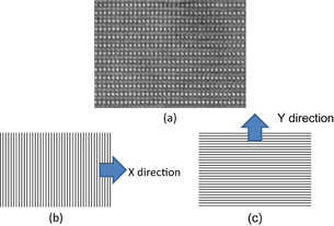
Fig. 4. Definition of principal directions of gratings in a crystal structure. (a) Crystal structure (enlarged TEM image). (b) X direction grating. The X direction is the principal direction. (c) Y direction grating. The Y direction is the principal direction.
Download figure:
Standard image High-resolution imageIn addition, the strain ε is calculated using

where p0 is the standard grid pitch (10.6 pixels in the X direction and 19.7 pixels in the Y direction in this study) and p is the actual grid pitch in each observed area. Furthermore, averaging filter processes within 33 × 33 pixels in the X direction and 59 × 59 pixels in the Y direction were applied to obtain strain maps.
3. Results and discussion
3.1. Moiré phases and dislocation maps with blanket samples
Figure 5 shows the analytical images of the as-epi sample. The original TEM image of the epitaxially as-grown AlGaN/GaN structure is shown in Fig. 5(a). The Moiré phase images in the X and Y directions, and defect distribution superposed on the original TEM image are shown in Figs. 5(b)–5(d), respectively. It is obvious that the location of defects is clearly detected from the discontinuous lines in the Moiré phases. Focusing on the defect distribution, some defects are concentrated along the AlGaN/GaN boundary, which can be attributed to the lattice mismatch between the AlGaN and the GaN crystals. Other defects distributed in the entire AlGaN and GaN areas are possibly point defects or edge dislocations originating from the epitaxial growth process. Hÿtch et al.33) reported that the displacement around an edge dislocation in silicon was successfully detected using a similar method, which is a combination of high-resolution electron microscopy and image analysis based on optical interferometry.

Fig. 5. TEM image, Moiré phase and defect distribution of blanket As-epi sample. (a) Original TEM image. (b) Moiré phase in the X direction. (c) Moiré phase in the Y direction. (d) Defect map.28)
Download figure:
Standard image High-resolution imageThe defect distributions of the after RIE and after wet treatment samples are shown in Figs. 6(a) and 6(b), respectively. With the after RIE sample, a 2–3-nm-thick amorphous layer was observed at the surface of the AlGaN film. Since we have already confirmed a high concentration of oxygen at the surface of this sample30,31) from prior X-ray photoelectron spectroscopy (XPS) measurements, this amorphous layer is thought to be an oxidized layer. Applying the 2D FFT sampling Moiré method, we confirmed that more than 200 defects were clearly observed along the amorphous/AlGaN boundary. Since RIE often induces damage in the plasma-exposed material as mentioned above, these defects are attributed to plasma-induced damage such as nitrogen vacancies and defects induced by ion collision. On the other hand, in the case of the after wet treatment sample, the amorphous layer was removed, resulting in a decrease in the number of defects along the amorphous/AlGaN boundary [Fig. 5(b)]. Therefore, it is confirmed that the wet treatment can effectively remove the defects in the plasma-damaged AlGaN layer as well as the thin amorphous (oxidized) layer.

Download figure:
Standard image High-resolution image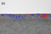
Fig. 6. Defect distribution in other blanket samples. (a) After RIE. (b) After wet treatment.28)
Download figure:
Standard image High-resolution imageThe decrease in the number of defects at the plasma-etched AlGaN film was also confirmed to cause improvement of capacitance–voltage (C–V) results in a basic test elemental group (TEG).30,31) A metal–insulating–semiconductor (MIS) capacitor TEG was fabricated on both after RIE and after wet treatment AlGaN/GaN samples for C–V measurements. As a result, the after RIE sample showed a positive threshold voltage shift and a deformation of the C–V curve caused by charge or electron traps generated during RIE, while the after wet treatment sample showed a much better C–V result. Thus, we firstly clarified the direct correlation between the improvement of electrical characteristics and the decrease in the number of defects in the GaN HEMT device structure. Thus, this Moiré phase analysis provides us with new and scientifically important information. The detailed discussion about defects observed in the bulk AlGaN/GaN layer will be described in the following section.
3.2. Dislocation maps with recessed samples
Figure 7 shows the results of the recessed AlGaN/GaN sample before thermal annealing. Using the same analytical procedure for the blanket samples, the Moiré phase images in the X and Y directions and defect distribution superposed on the original TEM image are obtained and shown in Figs. 7(b)–7(d), respectively. Thus, it is again confirmed that the defect distribution is clearly visualized even with a patterned sample by Moiré phase analysis. Figure 8 shows the defect distributions before and after thermal annealing. In both samples, the numbers of defects are observed in the bulk crystal as well as on the recessed surface. A numerical comparison is required for high-accuracy estimation and a more detailed discussion.

Fig. 7. TEM image, Moiré phase, and defect distribution of the patterned AlGaN/GaN sample without thermal annealing in NH3 ambient. (a) Original TEM image. (b) Moiré phase in the X direction. (c) Moiré phase in the Y direction. (d) Defect map. (Color bar from −π to π.)
Download figure:
Standard image High-resolution image
Fig. 8. Defect distribution in the patterned samples. (a) Before thermal annealing. (b) After thermal annealing.28)
Download figure:
Standard image High-resolution image3.3. Numerical evaluation of defects
To clarify the number and density of defects, defect counting was carried out using a new specific algorithm that was developed in this research. The number and density can be automatically calculated in a desired region within an obtained defect distribution image. In this study, we calculated the number and density of defects in two regions: one was on the surface corresponding to an area within approximately 2 nm from the actual surface, and the other was the bulk area except for the surface region. The image of the boundary line between the surface and bulk regions is shown in Fig. 9.
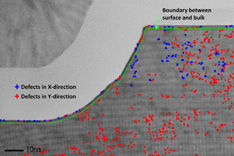
Fig. 9. Boundary line image between the surface region and the bulk region for quantitative estimation.
Download figure:
Standard image High-resolution imageThe results of all samples are summarized in Table II. Regarding the defect density in the blanket samples (As-epi, After RIE, and After wet treatment), the defect density at the surface region in the after RIE sample increased by about 3 times compared with that in the as-epi sample. However, the defect density at the surface region in the after wet treatment sample drastically decreased to 1/7. Thus, we succeeded in the quantitative estimation of defects, and again demonstrated that this wet treatment is effective for removing defects induced by plasma during RIE, as mentioned in Sect. 3.1. On the other hand, the defect density in the after wet treatment sample decreased by only 26% in the bulk region compared with the after RIE sample. When we again carefully investigate the defect maps of the after RIE and after wet treatment samples in Fig. 6, it is found that the defect distribution in the bulk regions shows no consistency, and it varies in different areas. This inconsistent and different defect distributions in the bulk is thought to originate from the epitaxial growth process of the AlGaN/GaN layer. The vertical continuous cluster of defects observed at the right-hand edge in Fig. 6(a) can be partially attributed to threading dislocations or screw dislocations. Since these dislocations are usually several µm in length, it is supposed that only a portion of the dislocations were observed in this highly magnified TEM image. Furthermore, the scattered defects shown in Fig. 6(b) are possibly point defects or edge dislocations as mentioned above. Although the scattered defects in Fig. 6(b) are concentrated in the AlGaN layer, no such concentration is observed in Fig. 6(a). To reveal the defect dislocation and to understand the origin of defects and dislocations, we require further observation of various epitaxially grown samples and additional verification by different approaches.
Table II. Defect count and density.
| Sample name | Number of defects | Defect density (counts/106 pixel2) | Defect density (×1013 counts/cm2) | |||
|---|---|---|---|---|---|---|
| Surface | Bulk | Surface | Bulk | Surface | Bulk | |
| As-epi | 73 | 793 | 260 | 72.5 | 3.79 | 1.06 |
| After RIE | 268 | 1185 | 712 | 70.9 | 18.2 | 1.88 |
| After wet treatment | 30 | 453 | 107 | 52.2 | 1.56 | 0.761 |
| Before annealing | 89 | 658 | 255 | 89.7 | 3.80 | 1.31 |
| After annealing | 102 | 647 | 235 | 62.6 | 3.45 | 0.914 |
Regarding the results of the recessed samples in Table II, only a slight decrease in the defect density is observed in the after annealing sample. Therefore, on the basis of this result, we were unable to confirm any significant effect of thermal annealing in NH3 ambient on the decrease in the number of crystalline defects induced by RIE plasma.
The defect densities in the unit of "counts/cm2" are also shown in Table II. The defect densities in Table II ranging from 7.61 × 10¹² to 1.82 × 10¹⁴ counts/cm2 are obviously several orders of magnitude higher than the usually accepted values. Further investigations are again required to obtain an overall understanding.
3.4. Strain maps
The 2D FFT Moiré method also enables us to obtain a strain map of an observed crystalline material based on Eq. (1). The strain maps of the blanket AlGaN/GaN samples (As-epi, After RIE, and After wet treatment) are shown in Fig. 10. The top three images show strain maps in the X direction, and the bottom images show those in the Y direction. In each map, the strain distribution in the AlGaN/GaN structure is clearly visualized with nm-scale spatial resolution. It is found that the highest strain reaches approximately 15% in the tensile direction (yellow sites), and that there is an inhomogeneous distribution of the strain with a size of a few nm. Such a high and inhomogeneous strain field is supposed to be caused by the lattice mismatch between the AlGaN, GaN, and Si(111) substrates.

Fig. 10. Strain distribution maps of blanket AlGaN/GaN samples. (a) As-epi, X direction. (b) As-epi, Y direction. (c) After RIE, X direction. (d) After RIE, Y direction. (e) After wet treatment, X direction. (f) After wet treatment, Y direction. (In the color bar, 0.15 corresponds to the right end.)
Download figure:
Standard image High-resolution imageRegarding the relationship between strains and defects, defect distributions are overdrawn in the obtained strain maps, as shown in Fig. 11, along with the original TEM images. Although most of the highly strained sites agreed with defect positions, some strained sites were formed without generating defects. Thus, it is revealed that highly strained AlGaN and GaN crystals still exist without generating defects and/or dislocations. In addition, the boundary of AlGaN/GaN can be identified in Figs. 11(b) and 11(f), and almost no defect is found along the boundary, which indicates that a well-ordered interface is realized in both as-epi and after wet treatment samples. Such a well-ordered interface is supposed to contribute to a well-regulated two-dimensional electron gas (2DEG) layer which determines the performance of GaN HEMT devices. In the case of the after RIE sample [Fig. 11(d)], the boundary of AlGaN/GaN is unclear, which indicates that the boundary has a disordered surface. Otherwise, the vertical continuous cluster of defects at the right-hand edge of the image may have some influence on the boundary condition. A highly strained area is observed at the AlGaN surface of the after RIE sample [Fig. 11(d)] although the strain at the AlGaN surface of the after wet treatment sample [Fig. 11(f)] is relatively small. This result indicates that this wet treatment can effectively decrease strains as well as the number of defects.

Fig. 11. Original TEM images, strain maps, and overdrawn defects of blanket AlGaN/GaN samples. Black dots represent defects. (a) As-epi, TEM image. (b) As-epi, strain and defect map in the Y direction. (c) After RIE, TEM image. (d) After RIE, strain and defect map in the Y direction. (e) After wet treatment, TEM image. (f) After wet treatment, strain and defect map in the Y direction. (In the color bar, 0.15 corresponds to the right end.)
Download figure:
Standard image High-resolution imageFurthermore, Fig. 12 demonstrates strain maps of the recessed sample. It is also confirmed that the strain maps are clearly visualized even with the patterned sample. Comparing the strain maps in the Y direction between before and after thermal annealing [Figs. 12(b) and 12(d)], we find that highly strained sites are scattered both in the AlGaN and GaN layers of the before annealing sample [Fig. 12(b)] while such sites are unevenly distributed in the GaN layer of the after annealing sample [Fig. 12(d)]. Such a change in defect distribution may be an effect of thermal annealing. Further study is required to clarify this observation.

Fig. 12. Strain distribution maps of patterned AlGaN/GaN samples. (a) Before annealing, X direction. (b) Before annealing, Y direction. (c) After annealing, X direction. (d) After annealing, Y direction. (In the color bar, 0.15 corresponds to the right end.)
Download figure:
Standard image High-resolution image3.5. Defect and strain maps of Si device
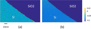
Finally, we discuss the possibility of utilizing this 2D FFT sampling Moiré method for other crystalline materials used in semiconductor devices. We introduce an analytical result for a silicon device in Fig. 13. Strain maps and the overdrawn defect distribution at a trench corner of the silicon device were also calculated and visualized from the original TEM image using the same procedure as described above. It is found that highly strained areas and defects are concentrated along the Si/SiO2 boundary, and that almost no defect or highly strained site is observed in the bulk Si crystal. Although the principal directions X and Y have an offset angle from the horizontal axis owing to the crystal orientation of Si(111), a coordinate transformation to the horizontal or vertical axis can be easily carried out using a reported equation.34) Thus, we believe that the 2D FFT sampling Moiré method has great potential applications to the discovery of as yet unknown relationship between the characteristics of a crystalline material and device performance.
Fig. 13. Strain and defects maps at a trench corner of a Si(111) device. (a) In the X direction (50° offset from the horizontal axis). (b) In the Y direction (140° offset from the horizontal axis). (In the color bar, −0.1 corresponds to the bottom end.)
Download figure:
Standard image High-resolution image
4. Conclusions
We applied the 2D FFT sampling Moiré technique to defect detection using GaN HEMT devices, and successfully and clearly visualized atom-size defects in AlGaN/GaN crystalline structures. The defect density obtained in the AlGaN/GaN structures is ∼1013 counts/cm2. In addition, we found that the distribution and number of defects closely depend on the process conditions. Thus, we confirmed that this technique is quite useful for device development. Moreover, the strain fields in the AlGaN/GaN crystal were successfully calculated with nm-scale resolution using this method. We also demonstrated that this sampling Moiré technique is applicable to silicon devices. Although the principal directions, X and Y, have an offset angle from the horizontal axis owing to the crystal orientation of Si(111), a coordinate transformation to the horizontal or vertical axis can be easily carried out using a reported equation. In conclusion, we believe that the 2D FFT sampling Moiré method has great potential applications for the discovery of an as yet unknown relationship between a crystalline material and device performance.
Acknowledgements
We thank Dr. Takeno of Toshiba Memory Corporation for his professional advice on TEM observation and discussion about the analytical results. We also thank Professor Hashizume of Hokkaido University for fruitful discussion.