

Abstract
CMOS miniaturization is now approaching the sub-10 nm level, and further downscaling is expected. This size scaling will end sooner or later, however, because the typical size is approaching the atomic distance level in crystalline Si. In addition, it is said that electron transport in FETs is ballistic or nearly ballistic, which means that the injection velocity at the virtual source is a physical parameter relevant for estimating the driving current. Channel-materials with higher carrier mobility than Si are nonetheless needed, and the carrier mobility in the channels is a parameter important with regard to increasing the injection velocity. Although the density of states in the channel has not been discussed often, it too is relevant for estimating the channel current. Both the mobility and the density of states are in principle related to the effective mass of the carrier. From this device physics viewpoint, we expect germanium (Ge) CMOS to be promising for scaling beyond the Si CMOS limit because the bulk mobility values of electrons and holes in Ge are much higher than those of electrons and holes in Si, and the electron effective mass in Ge is not much less than that in III–V compounds. There is a debate that Ge should be used for p-MOSFETs and III–V compounds for n-MOSFETs, but considering that the variability or nonuniformity of the FET performance in today's CMOS LSIs is a big challenge, it seems that much more attention should be paid to the simplicity of the material design and of the processing steps. Nevertheless, Ge faces a number of challenges even in case that only the FET level is concerned. One of the big problems with Ge CMOS technology has been its poor performance in n-MOSFETs. While the hole mobility in p-FETs has been improved, the electron mobility in the inversion layer of Ge FETs remains a serious concern. If this is due to the inherent properties of Ge, only p-MOSFETs might be used for device applications. To make Ge CMOS devices practically viable, we need to understand why electron mobility is severely degraded in the inversion layer in Ge n-channel MOSFETs and to find out how it can be increased. In the Si CMOS technology, the SiO2/Si interface has long been investigated and cannot be ignored even after the introduction of high-k gate stack technology. In that sense, the GeO2/Ge interface should be intensively studied to make the best of Ge's advantages. Therefore we first discuss the GeO2/Ge interface with regard to its physical and electrical characteristics. When we regard Ge as a channel material beyond Si for high performance ULSIs, we also have to seriously consider the gate stack scalability and reliability. The source/drain engineering, as well as the gate stack formation, is another challenge in Ge MOSFET design. Both the higher metal/Ge contact resistance and the larger p/n junction leakage current may be the consequences of Ge's intrinsic properties because they are derived from the strong Fermi-level pinning and the narrow energy band gap, respectively. Even if the carrier transport in the channel may be ideally ballistic, these properties should degrade FET properties. The narrower energy band gap of Ge is often addressed, but the higher dielectric constant of Ge is rarely discussed. This is also the case for most of the other high-mobility materials. The dielectric constant is directly and negatively related to short-channel effects, and we have not been able to provide a substantial solution to overcome this hardship. We have to keep this in mind for the short-channel FET operation. Although a number of problems remain to be solved, in this paper, we view the current status of Ge FET technology positively. A number of (but not all) Ge-related challenges have been overcome in the past 10 years, which seems to be a good time to summarize the status of Ge technology, particularly materials engineering aspects rather than device integration issues. Since we cannot cover all of the results published to date, we mainly discuss fundamental aspects based on our experimental results. Remaining challenges are also addressed but not comprehensively. Integration issues are not discussed in this review. Finally, new types of electron devices utilizing Ge's advantages are briefly introduced on the basis of our experimental results.
Export citation and abstract BibTeX RIS
Table of contents
1. Introduction
2. Stabilizing GeO2/Ge gate stacks
2.1 Thermodynamics and kinetics of GeO desorption
2.2 Thermodynamic approach
2.2.1 High-pressure O2 oxidation
2.2.2 GeO2/Ge MOS capacitors
2.2.3 Defects in bulk GeO2
2.3 Kinetic approach
2.4 Materials approach
2.5 Oxidation kinetics of Ge
3. Enhancing electron mobility in Ge MOSFETs
3.1 Dit reduction
3.2 Substrate surface orientation
3.3 Atomically flat Ge surface
3.4 Defects in Ge substrate
4. Scaling EOT
4.1 Low-temperature high-pressure O2 oxidation
4.2 Low-oxygen-potential oxides
4.3 High-k material selection for further EOT scaling
5. Assuring Ge gate stack reliability
5.1 Initial traps and trap generation
5.2 Network flexibility and rigidity
5.3 Reliable scaled Ge gate stacks
6. Reducing contact resistance and junction leakage
6.1 Schottky barrier height control
6.1.1 Fermi-level pinning modulation: tunnel contact
6.1.2 Fermi-level pinning modulation: electron density tuning in metals
6.2 n+/p junction
7. Setting new devices
7.1 ET-GeOI FET
7.2 Metal source/drain FET
7.3 Junctionless FET
7.4 New field effect on Ge
8. Conclusions and future outlook
1. Introduction
Si CMOS miniaturization is currently approaching the 7 nm node not in a single FET operation but in the integration level.1,2) Nevertheless, planar FET size scaling including FinFET will eventually end because there is a physical limit of the distance between neighboring atoms, so FET performances have to be improved by other ways. System performance will be improved by using three-dimensional rather than two-dimensional integration, and high-mobility channel semiconductors have always been desired for high-speed and/or low-power applications. It is, however, not easy to implement new materials in the current Si-LSIs. Furthermore, FET performance will be limited by the ballistic transport in the channel, and the ultimate carrier speed will depend on the injection velocity near the source side.3,4) Whether the ultimate performance of FETs is related to the carrier mobility or not is often discussed, and here, we note that the injection velocity is related to the mobility because both properties depend on the carrier's effective mass. It has been shown experimentally that a higher mobility is needed to achieve a higher injection velocity.5)
Various materials have been proposed for high-mobility channels beyond Si. Look at the bulk electron and hole mobility values in Table I. Note that germanium (Ge) shows the most balanced electron and hole mobility values. The monoatomic semiconductor nature of Ge should also be emphasized because the characteristics of a compound semiconductor are rather sensitive to its stoichiometry. The density of states in the channel is also relevant for estimating the channel current because it is directly related to the gate capacitance.6) Both the density of states and high mobility in the channel are related to the effective mass of the carriers. From this device physics viewpoint, we expect that Ge CMOS is most promising for "beyond Si-CMOS" scaling. On the other hand, it has been said that Ge should be used for p-MOSFETs and III–V compounds for n-MOSFETs.7,8) In fact, a critical technology selection according to the applications might be needed, but when it is considered that a big challenge in the current CMOS LSIs comes from the variability or nonuniformity of the FET performance in them, it seems that much more attention should be paid to the simplicity of the material design and of the processing steps.
Table I. Carrier mobility, effective mass and energy band gap in bulk Si, Ge, and typical III–V compound semiconductors. A very high hole mobility in Ge is far ahead of others.
| Si | Ge | GaAs | InP | InAs | InSb | |
|---|---|---|---|---|---|---|
| Electron mobility (cm2 V−1 s−1) | 1600 | 3900 | 9200 | 5400 | 40000 | 77000 |
| Electron effective mass (/m0) | mt: 0.19 ml: 0.916 | mt: 0.082 ml: 1.467 | 0.067 | 0.082 | 0.023 | 0.014 |
| Hole mobility (cm2 V−1 s−1) | 430 | 1900 | 400 | 200 | 500 | 850 |
| Hole effective mass (/m0) | mHH: 0.49 mLH: 0.16 | mHH: 0.28 mLH: 0.044 | mHH: 0.45 mLH: 0.082 | mHH: 0.45 mLH: 0.12 | mHH: 0.57 mLH: 0.35 | mHH: 0.44 mLH: 0.016 |
| Energy band gap (eV) | 1.12 | 0.66 | 1.42 | 1.34 | 0.36 | 0.17 |
A number of research outputs on Ge have been so far reported and both its advantages and disadvantages have been discussed considerably.9,10) Although our objective is to realize high-performance Ge CMOS LSIs with a realistic shape, Si CMOS LSIs will not disappear and new Ge devices will coexist with Si devices. New materials might thus not necessarily be used for all of the functions in LSIs, but the total system performance should be improved by using their advantageous aspects. If the advantages of Ge are not exploited, Ge will lose its original appeal.
Germanium was discovered in 1886 by Winkler,11) the first transistor was demonstrated on Ge in 1947 by Bardeen, Brattain, and Shockley,12) and the first integrated circuit (IC) was demonstrated on Ge in 1958 by Kilby.13) The electric properties of Ge were reported in depth approximately 100 years ago.14) Thus Ge is obviously not a new electron-device material but has been "sleeping" for half a century even though there have of course been strong demands for nuclear radiation spectrometers and IR detectors. Now, it is waking up from its long sleep and is attracting much attention. Although there might be a number of apparently intrinsic challenges, for most of them, we may find solutions on the basis of present in-depth understandings of materials science and device physics. This optimistic view is held throughout this paper.
Nevertheless, we have to remind ourselves what problems there were in the past before the Si era. Historical details of Ge and Si research in the early stage of electron device research and development are interestingly described in Ref. 15, which points out several reasons that Si has become the mainstream material for electron devices.
- (i)Si is abundant on Earth.
- (ii)The operation temperature range is wider in Si than in Ge.
- (iii)Purer crystals can be obtained in Si than in Ge.
- (iv)Single crystalline Si is produced on an industrial scale.
- (v)SiO2 is a very stable material for the surface passivation.
It is easily understandable that those reasons were critical for the successful production of reliable devices. Conversely speaking, they are problems that must be solved if Ge is to overcome Si. Since (i) and (ii) are owing to inherent properties (Clarke number and energy band gap), it seems impossible to solve them. However, Ge is not a rare material and it should be used only in parts of devices where it is advantageous rather than for all purposes. We should keep in mind that a high junction leakage current is potentially a big concern in any devices even at room temperature. (iii) is related to defect control in the Ge crystallinity. This is a big concern in ULSI, but the crystal purity has been improved a lot. (iv) is related to how to use Ge. Since it is now considered that Si will be used as the bottom substrate, the possible wafer size of Ge is not necessarily a big concern. (v) is still a serious challenge in the device fabrication process because we know that a key to fabricating high-performance FETs is understanding how to control any hetero interfaces. As discussed later, GeO2 is not stable, which was well known and investigated even before the Si era,16) and we cannot simply mimic the successful SiO2/Si technology. Thus, Ge gate stack and passivation technologies should be studied deeply and carefully when Ge is considered for use as a "beyond Si" channel material.
Let us start here by showing some general material properties of Ge. Figure 1(a) shows the electronic structure of Ge, which is fundamental for considering device physics. In addition to the band gap being narrower than that of Si, the direct band gap at the Γ-point is significantly smaller in Ge than in Si. This is very important for the optical applications of Ge. It is interesting to see the difference between the electron configurations of Si and Ge atoms as shown in Fig. 1(b). In fact, 3d electrons in Ge affect the energy levels of 4s and 4p electrons and the 4s electron level is rather deep because 3d electrons cannot fully screen the inner shell. The Clarke number of Ge shows that Ge is the 43rd most abundant element on Earth, whereas Si is the second most abundant. Ge has several kinds of isotopes with different mass numbers, and they are discussed later in the context of marker experiments. The material properties of Ge are summarized in Table II, where they are compared with those of Si.

Download figure:
Standard image High-resolution image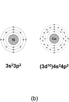
Fig. 1. (a) Electronic structure of Ge. The conduction band minimum is located at L-point with an indirect energy band gap of 0.66 eV. The direct energy band gap at the Γ-point is about 0.80 eV, which is rather close to the indirect one. This is in striking contrast to the Si case. (b) Schematic electron configurations of Si and Ge atoms. The 4s state of Ge is rather deep compared with the 3s state of Si because of the insufficient screening by 3d electrons.
Download figure:
Standard image High-resolution imageTable II. Typical material properties of Ge and Si. All of them listed in this table in addition to carrier mobility should be considered for designing real electron devices.
| Ge | Si | |
|---|---|---|
| Density (g/cm3) | 5.327 | 2.328 |
| Young's modulus (N/m2) 〈100〉 direction | 1.3 × 10¹¹ | 1 × 10¹¹ |
| Thermal conductivity (W cm−1 K−1) at 300 K | 0.6 | 1.5 |
| Dielectric constant | 16.0 | 11.9 |
| Refractive index at 633 nm | 5.48 | 3.88 |
| Lattice constant (Å) | 5.64613 | 5.43095 |
| Clarke number (%) | 0.00065 | 25.8 |
This review consists of eight sections, but by and large, it can be divided into two parts. The first part is on the gate stacks. Ge oxidation stabilizing the Ge interface is discussed in Sect. 2 because GeO2/Ge is the basis for Ge gate stacks. Through this investigation, a big difference between the oxidation processes of Ge and Si is discussed thermodynamically. On the basis of this understanding, markedly improved Ge MOS capacitor characteristics are presented. In addition, high-performance n-channel Ge FET properties that will make high-performance Ge CMOS devices possible are demonstrated in Sect. 3. This part naturally extends to cover the high-k/Ge systems needed to meet the scalability requirements discussed in Sect. 4. Furthermore, the assurance of gate stack reliability is needed for the practical application of Ge devices. This will be discussed in Sect. 5 by introducing a new reliability concept. The second part of this review is on the source/drain formation, including metal/Ge contact. This formation process is still under investigation, but we would like to share our views about this issue. In particular, the very strong Fermi-level pinning (FLP) in metal/Ge contacts is unique to Ge and is discussed in Sect. 6. The final section discusses new types of devices exploiting specific advantages of Ge. Although the Roadmap issues17) are often discussed extensively in the introductory part of review papers, in this review, we instead focus on the material aspects of the Ge CMOS process and device technology.
We would like to present our views, based on material properties and thermodynamic considerations, concerning mainly both how to improve Ge gate stacks and how to control the perfect FLP on Ge by material science based engineering. Of course, there may be other ways to obtaining high-performance Ge FETs, but we hope that guidelines based on the material and thermodynamic aspects considered in this paper will be useful to anyone working on Ge or new channel materials.
2. Stabilizing GeO2/Ge gate stacks
First let us discuss how to achieve excellent Ge gate stacks with GeO2/Ge without considering any other concerns such as scalability or reliability. We should pay attention to the GeO2/Ge interface because the SiO2/Si interface is still the heart of Si-CMOS gate stack technology even after metal gate/high-k gate stacks have been introduced.
The parabolic law of the thermal oxidation for Ge was also reported18,19) as the Deal–Grove model for Si,20) but this does not mean that GeO2/Ge might be the same as SiO2/Si. This is not the point for achieving wonderful gate stacks. Although the Ge oxidation kinetics will be discussed later, a big difference between the device-process technology for Ge and that for Si is that significant GeO desorption from the GeO2/Ge stack should be taken into consideration.21) On the other hand, high-temperature oxidation is desirable as far as GeO2 quality is concerned because GeO2, like SiO2, has the continuous random network type of structure and the network in the whole film should be completely be stabilized. Understanding and controlling the GeO desorption from the GeO2/Ge stack are therefore of vital importance.
2.1. Thermodynamics and kinetics of GeO desorption
GeO desorption from GeO2 was directly investigated using thermal desorption spectroscopy (TDS) measurements22,23) carried out in ultrahigh vacuum (UHV) at high temperatures,24) because GeO desorption from ultrathin GeO2 on Ge in UHV was reported to occur at temperatures above 400 °C.25) In fact, GeO desorbs from the GeO2/Ge stack at a relatively low temperature but, interestingly, not from GeO2/SiO2 stacks shown in Fig. 2. This indicates that the GeO desorption is directly related to a reaction that triggers GeO desorption at the GeO2/Ge interface.
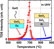
Fig. 2. Thermal desorption spectra of GeO (m/z = 86, 88, 89, 90, and 92; where m and z are respectively the desorbed species mass and electronic charge) desorbed from GeO2/Ge and GeO2/SiO2/Si stacks in UHV. It is inferred that the GeO desorption is triggered by the GeO2/Ge interface reaction.26)
Download figure:
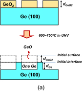
Standard image High-resolution imageFigure 3 shows both (a) schematic cross sections of a GeO2 line-and-space pattern on Ge before and after UHV annealing and (b) the atomic force microscope (AFM) image of the pattern after UHV annealing.26) The Ge substrate is consumed only underneath GeO2 lines, indicating that GeO desorption is caused by a GeO2/Ge reaction. Another aspect of the GeO desorption is shown in Fig. 4, where (a) is a schematic image of a SiO2 line-and-space pattern on Ge before N2 annealing and (b) shows AFM cross-sectional images of the pattern before and after N2 annealing at 600 °C.26) Since N2 gas actually included a small amount of O2, Ge was consumed only where it was not under SiO2. This is a typical example of the active oxidation.
Download figure:
Standard image High-resolution image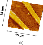
Fig. 3. (a) Schematic images of a line-and-space patterned GeO2 on Ge expected before and after annealing in UHV. Ge covered with GeO2 is only consumed in UHV-PDA. (b) Top-view AFM image of GeO2/Ge after annealing in UHV. This result clearly shows that GeO desorption is induced by the reaction of GeO2 with Ge.26)
Download figure:
Standard image High-resolution image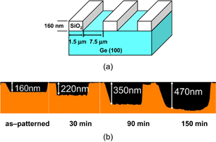
Fig. 4. (a) Schematic image of a line-and-space patterned SiO2 on Ge. (b) Cross-sectional height profiles inspected by AFM of samples as-patterned and annealed at 600 °C in N2 for 30, 90, and 150 min. Ge is etched by the remaining O2 in N2, which is a typical example of active oxidation.26)
Download figure:
Standard image High-resolution imageConsidering that GeO desorption is associated with the reaction at GeO2/Ge as shown above, we suggest the following net reaction.

Next, let us think about what is the difference between Ge oxidation and Si oxidation thermodynamically. Vapor pressures of the volatile species Ge(g), GeO(g), and GeO2(g) in the Ge-and-O2 system as well as their Si counterparts in the Si-and-O2 system under a thermodynamic equilibrium condition27) were first calculated using a thermodynamic database.28) The equilibrium vapor pressures of GeO(g), GeO2(g), and Ge(g) (p-GeO, p-GeO2, and p-Ge, respectively) are shown in Fig. 5(a) as a function of the p-O2 at 550 °C. Similar reactions were calculated for Si at 900 °C, as shown in Fig. 5(b). The Si results are the same as reported elsewhere.29) Note that the system temperatures for both Ge and Si were ∼0.7 × TM (TM; melting temperature), which are typical temperatures used for the dry oxidation of these semiconductors. At p-O2 < 10−26.3 atm, GeO(g), GeO2(g), and Ge(g) equilibrate with Ge(s) in the following reactions.
GeO(g) and GeO2(g) equilibrate with GeO2(s) at p-O2 > 10−26.3 atm.
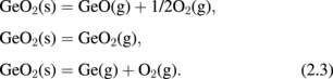
Three important points in Fig. 5 are the following:
- (i)p-GeO is the highest at the GeO2/Ge interface up to p-O2 ∼ 1 atm,
- (ii)p-GeO has a negative slope against p-O2, and
- (iii)p-GeO is comparable with p-GeO2 at p-O2 ∼ 1 atm.
Looking at the p-O2 ∼ 1 atm region in Fig. 5(a), one clearly sees that the p-GeO is much higher than that of SiO in Fig. 5(b), in addition to (iii). This means that GeO desorption from GeO2/Ge observed experimentally is thermodynamically reasonable. Furthermore, a negative slope of p-GeO against p-O2 suggests that GeO desorption from the surface may affect the region deep inside GeO2 film and degrade both bulk and interface of GeO2/Ge system. On the other hand, since p-GeO decreases with increase in p-O2, the high-pressure O2 oxidation might be effective for growing SiO2-like GeO2, which is discussed in the next section.
Download figure:
Standard image High-resolution image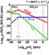
Fig. 5. (a) Equilibrium vapor pressure of GeO(g), GeO2(g), and Ge(g) at 550 °C as a function of O2 pressure (p-O2). (b) Equilibrium vapor pressure of SiO(g), SiO2(g), and Si(g) at 900 °C as a function of p-O2. 550 °C is 0.7 × TM(Ge) and 900 °C is 0.7 × TM(Si), where TM(Ge) and TM(Si) are the melting temperatures of Ge and Si, respectively. It is noted that 550 and 900 °C are also typical oxidation temperatures for Ge and Si, respectively. At p-O2 = 1 atm, the vapor pressure of GeO is significantly higher than that of SiO.27)
Download figure:
Standard image High-resolution imageNext, the GeO desorption kinetics is experimentally discussed. As shown in Fig. 6, the temperature giving a peak in TDS increases with the GeO2 thickness increase, while it little depends on how GeO2 is formed.30) This fact suggests that the GeO desorption is limited by diffusion through the bulk GeO2 network. It might be, however, unlikely that GeO is the diffusion species. To clarify the diffusion species and mechanism, isotope tracing experiments using 18O and 73Ge were carried out with TDS and secondary ion mass spectroscopy (SIMS).30) 73Ge was used for these experiments because it is an only Ge isotope with an odd mass number and thus easier to trace in the marker experiments. Two kinds of gate stack structures focusing on 18O and 73Ge were prepared, as shown in Fig. 7(a). The Ge16O is desorbed at a lower temperature, as shown in Fig. 7(b), which suggests that O of desorbed GeO is not from the interface but from the top layer. It was also suggested that Ge of desorbed GeO was also from the top layer (data not shown). Results point out that both Ge and O are desorbed from the top surface of GeO2 at the initial stage in the temperature sweep. This initial desorption from the top layer seems inconsistent with GeO desorption being triggered by the GeO2/Ge reaction as discussed previously. However, it is understandable by considering that the oxygen atom diffuses from the top layer toward the interface, namely, oxygen vacancy (Vo) diffusion from the GeO2/Ge interface to the top surface. To determine the actual diffusion species through the GeO2 film, the sample structure shown in Fig. 8(a) was prepared using both 73Ge and 18O, and then annealed at 600 and 650 °C. Figures 8(b) and 8(c) show that the O atom is the dominant diffusion species in GeO2.30) It is actually regarded that Vo is formed through the reaction at the interface,

Namely, the Ge substrate is oxidized by GeO2 at the interface, while at the surface,

In the net reaction,

The Vo formation triggered by the oxidation in (2.4) drives GeO desorption through the Vo diffusion.30) Figure 9 is more intuitively helpful to understand what occurs inside the GeO2 film on a Ge substrate. This kinetic view is the key concept when we treat GeO2/Ge gate stacks.

Download figure:
Standard image High-resolution image
Fig. 6. (a) TDS intensity of GeO (m/z = 86, 88, 89, 90, and 92) desorbed from sputtered GeO2 on Ge stacks with various GeO2 thicknesses. A thinner GeO2 on Ge shows a lower desorption temperature. (b) Peak desorption temperature in TDS as a function of initial thickness of differently grown GeO2. There is no considerable difference of GeO desorption temperature for GeO2 grown differently on Ge. This fact suggests that a diffusion process in GeO2 is not through a pin-hole but occurs uniformly in the GeO2 film.23,26)
Download figure:
Standard image High-resolution image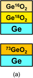
Download figure:
Standard image High-resolution image
Fig. 7. (a) Schematics of sample structures used in the isotope tracing experiments investigating GeO desorption. Two types of samples were prepared using 18O and 73Ge. (b) Typical TDS results of GeO from Ge16O2/Ge18O2/Ge. Each GeO2 thickness was ∼17 nm. Ge16O was interestingly observed at lower temperature than Ge18O existing at the interface. In case of 73GeO2/Ge, 73GeO was detected at lower temperature, though the reaction should occur at the interface (data not shown for the 73GeO desorption).
Download figure:
Standard image High-resolution image
Download figure:
Standard image High-resolution image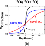
Download figure:
Standard image High-resolution image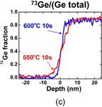
Fig. 8. (a) Schematic sample structure for determining the diffusion species through GeO2. SIMS profiles of (b) 18O and (c) 73Ge in the sample annealed at 600 and 650 °C in N2. The O atom is the dominant diffusion species in GeO2 at around 600 °C.30)
Download figure:
Standard image High-resolution image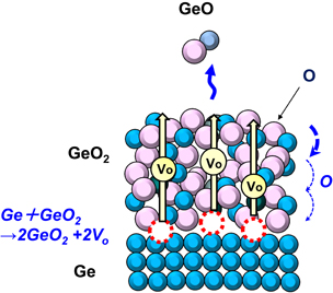
Fig. 9. A kinetic model proposed for the GeO desorption. For understanding the above experimental results, it is most probable that Vo diffusion from the GeO2/Ge interface triggers GeO desorption at the top surface.30) It is uncertain whether the oxygen vacancy Vo in amorphous GeO2 can be well defined, but we will use the Vo although it might be slightly different from Vo in crystalline materials.
Download figure:
Standard image High-resolution imageGeO2 film properties were affected by UHV annealing through the above process. Figures 10(a) (X-ray diffraction, XRD) and 10(b) (transmission electron microscope, TEM)31) show that GeO2 on Ge in UHV-annealing at 660 °C is crystallized to an α-quartz type structure.32) This is also understandable by considering the reduction in the crystallization barrier energy with the help of the Vo diffusion in GeO2. This seems quite interesting from the viewpoint that Vo's make the continuous random network (CRN) type of GeO2 structure unstable. In fact, if oxygen atom diffusion can follow the Vo diffusion instantaneously, GeO desorption associated with Vo diffusion may be observed. However, if huge amounts of Vo's are generated under the UHV condition, it is likely that the CRN structure of the GeO2 film may be collapsed and crystallized locally. Those properties in GeO2/Ge are quite different from those in SiO2/Si stacks and, as discussed later, are tightly related to the GeO2 physical properties.

Download figure:
Standard image High-resolution image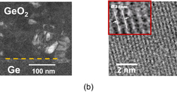
Fig. 10. (a) XRD patterns of GeO2/Ge(100) and GeO2/SiO2/Si stacks after UHV-PDA at 660 °C for 1 min. 230-nm-thick GeO2 was deposited by rf-sputtering. The former sample was only crystallized to a quartz type of GeO2 in UHV-PDA. (b) Cross-sectional TEM images of GeO2 film on Ge(100) after the UHV-PDA. GeO desorption may help to crystallize GeO2 film.31)
Download figure:
Standard image High-resolution imageBecause oxygen vacancies are always involved both at the interface and in the bulk GeO2, we have to suppress the GeO desorption if we wish to make excellent gate stacks on Ge. There are basically two ways of solving this problem: thermodynamically and kinetically. The kinetic approach was actually carried out first, but we start with discussing the thermodynamic approach, because the thermodynamic one has been more successful and investigated in much more detail. The kinetic one is discussed in Sect. 2.3, after which the material approach combining both of them is discussed in Sect. 2.4.
2.2. Thermodynamic approach
2.2.1. High-pressure O2 oxidation.
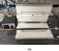
We first tried to form GeO2 thermally under 1 atm O2 but were not satisfied with the results. We naively conjectured that the high-pressure O2 (HPO) oxidation might be effective for suppressing the GeO desorption because we thought enough O2 could reduce the amount of insufficiently oxidized GeOx in the film. Therefore, before considering the thermodynamics of Ge oxidation as described in Sect. 2.1, we carried out the oxidation of Ge in a high-pressure O2 ambient. Since it was not possible to use the conventional quartz furnace for the oxidation at pressures above 10 atm, a stainless chamber with a quartz tube as the inner wall was used for the oxidation as shown in Fig. 11(a). Then, a SUS tube was directly put into the conventional open furnace. The schematic image of the oxidation system is shown in Fig. 11(b). Since it was a very simple system, the actual p-O2 in it could not be directly measured at elevated temperatures. However, because the p-O2 measured after the oxidation was the same as the initial p-O2, only a very slight O2 leakage (if any) in this process was confirmed and the actual p-O2 was estimated according to the Boyle-Charles's law. The p-O2 at the oxidation temperature around 600 °C was estimated from the typical p-O2 of ∼70 atm at room temperature to be roughly 200 atm. p-O2 in this paper is hereafter denoted by the room-temperature p-O2. Although this tube is obviously not suitable for use in the industrial-scale production, we have learned much from these experiments. Very fortunately, in the first HPO experiment, we were able to demonstrate surprisingly good MOS capacitor characteristics with HPO-grown GeO2 on Ge.33) Details of electrical characteristics are discussed in the next section.
Download figure:
Standard image High-resolution image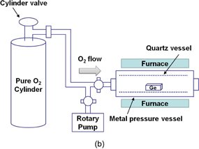
Fig. 11. (a) Photograph of a home-made high-pressure O2 annealing furnace. (b) Schematic image of high-pressure O2 annealing system. Since it is difficult to measure the actual O2 pressure (p-O2) at elevated temperatures, p-O2 at room temperature is referred throughout this paper.
Download figure:
Standard image High-resolution imageLow-temperature HPO of Si at pressures up to 500 atm was reported a couple of decades ago to prepare high-density SiO2 films of sufficient thickness.34) Later, a more practical furnace was used to study the HPO oxidation of Si at pressures up to 10 atm in a quartz tube.35) Although we did not know that high-pressure O2 oxidation of Ge was carried out in the early 80's by Crisman and coworkers,36,37) before our first demonstration of significantly improved capacitance–voltage (C–V) characteristics in HPO-grown GeO2/Ge gate stacks,33) they surprisingly demonstrated Ge gate stack improvement by using very high pressure O2 gas. Therefore, we should appreciate their original work on the HPO oxidation of Ge.
2.2.2. GeO2/Ge MOS capacitors.
As expected from the thermodynamic consideration discussed previously, the HPO of Ge dramatically improved the Ge MOS capacitor characteristics.38) Furthermore, because the C–V characteristics of HPO-grown GeO2/Ge MOS capacitors showed a slight hysteresis, we tried to annihilate the interface defects by post-oxidation annealing (POA) at a lower temperature (400 °C). This POA was carried out using H2, N2, and O2. As seen when comparing Figs. 12(a) and 12(b), we found that O2 POA at a lower temperature was quite effective in improving C–V characteristics.39) Hereafter, we call it low-temperature oxygen annealing (LOA). The LOA was actually carried out at 400 °C in 1 atm O2 after the formation of high-quality bulk GeO2 by HPO at 550 °C. This process is hereafter called HPO+LOA.
Download figure:
Standard image High-resolution image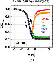
Fig. 12. Bidirectional C–V characteristics of Au/GeO2/p-Ge(100) MIS capacitors, where GeO2/Ge stacks were fabricated by (a) HPO at 550 °C for 15 min and (b) HPO at 550 °C for 15 min + LOA at 400 °C for 30 min. Although both exhibit good C–V characteristics, the C–V hysteresis is much reduced by adding the LOA.38,39)
Download figure:
Standard image High-resolution imageThe effectiveness of LOA was also thermodynamically justified as follows. Note that the p-GeO at the GeO2/Ge interface is thermodynamically fixed, independent of the p-O2 at a given temperature, because of the Gibbs's phase rule. Interface properties can therefore be further improved, without degrading bulk GeO2 properties, by lowering the temperature. It was actually confirmed by the calculation that p-GeO was decreased by lowering the temperature in 1 atm O2.27) This means that improving MOS C–V characteristics by LOA in Fig. 12(b) is thermodynamically reasonable. Thus, it is concluded with confidence that the wonderful MOS gate stacks on Ge can be made by suppressing the GeO desorption from GeO2/Ge gate stacks.
Next, we quantify how the interface is improved by estimating the interface state density Dit. Those who are not familiar with the C–V characteristics of Ge MOS capacitors might think that the minority carrier response in the inversion region at low frequencies in Fig. 12 is huge and that Dit should be high. This is not true. It is due to the intrinsic bulk minority carrier response in the Ge bulk with the narrower energy band gap. This means that characterization methods usually available for estimating the Dit in Si MOS capacitors cannot be used in Ge cases. For example, the conductance method in which the minority carrier capture and emission only from interface states are assumed40) is widely used for estimating the Dit spectrum in Si MOS capacitors quantitatively. In the C–V characterization of Ge MOS capacitors, however, the bulk minority carrier generation needs to be taken into account. Therefore, if we apply the normal conductance method to Ge MOS capacitors at room temperature, we would have a big error in the Dit estimation. There are two ways to overcome this difficulty. One is to lower the measurement temperature, because lowering the temperature must reduce the minority carrier generation in the bulk exponentially. The other is to develop a new equivalent circuit model to describe Ge MOS capacitor characteristics at room temperature. The equivalent circuit was carefully developed by Fukuda et al.41) and Martens et al.42) We employed the former method because it was experimentally straightforward.
Figure 13 shows Dit profiles estimated by the conductance method. They are the profiles estimated at 200 and 100 K in MOS capacitors with GeO2/Ge(100) grown both by HPO and by HPO+LOA. The midgap Dit is on the order of 1010 cm−2 eV−1 in HPO+LOA,39) which is to our knowledge the lowest of midgap Dit values so far reported for Ge gate stacks. Note that forming gas annealing (FGA) was not employed for reducing Dit. The reason why the oxidation process can make Ge interface quality so remarkable may be that Ge–O bonds at the GeO2/Ge interface are more flexible than Si–O bonds at the SiO2/Si interface. Therefore we regard the LOA as the self-passivation of the GeO2/Ge interface by oxygen itself rather than H2 gas in FGA. The effectiveness of aforementioned oxidation process may also be understandable in conjunction with the viscoelastic properties of GeO2.43)
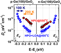
Fig. 13. Energy distributions of Dit inside the energy band gap, estimated by the low-temperature conductance method at 200 and 100 K for two kinds of Au/GeO2/p-Ge(100) capacitors. GeO2 films were grown by HPO and by HPO+LOA. Ei is the midgap position in the energy band gap. Both Dit profiles exhibit the so-called U-shape distributions inside the energy band gap. Dit values are much lower in the HPO+LOA case, and the midgap Dit in HPO+LOA is below 1011 cm−2 eV−1, without any passivation process.39)
Download figure:
Standard image High-resolution imageThe FGA effect on GeO2/Ge interfaces is still under debate in related conferences. Our experiments have never shown any Dit improvements in the FGA, although annealing temperature effects have been observed occasionally. It was also reported that H-terminated Ge(100) was unstable.44) However, hydrogen is a tricky atom, so we need to carefully investigate it in more detail, including deuterium or radical effects.45)
The surface orientation of the substrate is always an issue in surface channel FETs in terms of both process stability and carrier mobility. Since the carrier mobility is discussed in Sect. 3.2, the process sensitivity and MOS capacitor characteristics are addressed here. The oxidation rates of Ge(100) and (111) under 1 atm O2 at 600 °C are shown in Fig. 14 as a function of oxidation time. The oxidation rate of Ge(111) is much lower than that of (100).39) This suggests that Ge(111) would be better in terms of GeO2 scalability as the interfacial layer of high-k dielectric film. Furthermore, the substrate orientation dependence of the GeO desorption was also investigated after depositing 30-nm-thick GeO2 on Ge(100) and (111) wafers. Figure 15 shows that the GeO desorption temperature is much higher on (111) than on (100),30) and these results strongly suggest that Ge(111) is superior to Ge(100) with regard to the rate of GeO desorption under a given process condition. Concerning the interface, no significant Dit difference between Ge(100) and Ge(111) was observed when examining the C–V characteristics of MOS capacitors made using the HPO+LOA process.39)

Fig. 14. GeO2 thickness on Ge(100) and (111) surfaces grown in 1 atm O2 at 600 °C is plotted as a function of oxidation time. Ge(111) has a lower oxidation rate.39)
Download figure:
Standard image High-resolution image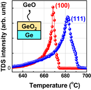
Fig. 15. TDS results for GeO desorbing from 30-nm-thick GeO2 on Ge(100) and (111) are shown. Ge(111) is more robust against GeO desorption.30)
Download figure:
Standard image High-resolution image2.2.3. Defects in bulk GeO2.
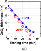
Note that the quality of not only the interface but also the bulk GeO2 film grown in HPO is greatly improved. Figure 16 shows that (a) the water etching rate is slightly less in HPO-GeO2 and that (b) C–V hysteresis increases with the time left in the air more clearly in APO-GeO2 (APO: atmospheric pressure O2) than in HPO-GeO2. These facts indicate that the HPO process densifies the GeO2 film and reduces the amount of electrical traps in it. The density increase of HPO-GeO2 directly detected by the grazing incident X-ray reflectivity (GIXR) measurement is shown in Fig. 17.46)
Download figure:
Standard image High-resolution image
Fig. 16. (a) Etching rate of HPO- and APO-grown GeO2 films by alcohol-diluted H2O. HPO-grown GeO2 is more tolerant against H2O etching than APO-grown GeO2. (b) Relationship between air exposure time and the C–V hysteresis in HPO+LOA and APO+LOA GeO2/Ge stacks. HPO+LOA samples are clearly more robust with regard to their C–V hysteresis.
Download figure:
Standard image High-resolution image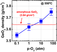
Fig. 17. Density of GeO2 film estimated by GIXR as a function of oxygen pressure p-O2. The density of the GeO2 film oxidized at 550 °C clearly increases with increasing p-O2. Note that p-O2 plotted here is the O2 pressure at room temperature.46) No density change has been reported for SiO2 in HPO oxidation of Si.35)
Download figure:
Standard image High-resolution imageWe suspect that APO-grown GeO2 films may have Vo-induced voids in it. Figure 18 shows the impact of PDA on GeO2 film properties, evaluated by the band-edge photo-absorption with spectroscopic ellipsometry.23) An appreciable subgap (band edge tailing) formation is observed in N2- or APO-PDA cases but not in HPO-PDA. The optical band gap of HPO-GeO2 is estimated to be ∼6.0 eV. This suggests that the subgap formation may be related to oxygen deficiency in the GeO2 film. Looking at the spectra more carefully, one can see that the subgap absorption seems to consist of two peaks at ∼5.1 and ∼5.8 eV. Those peaks might be correlated with defects such as neutral O vacancies or Ge2+, which was reported as a plausible origin of ∼5 eV photo-absorption observed in oxygen-deficient GeO2 bulk glass.47) Furthermore, subgap formation was not detected in GeO2 deposited on SiO2 (data not shown). Therefore, the oxygen deficiency is closely related with the interface reaction discussed in Sect. 2.1.
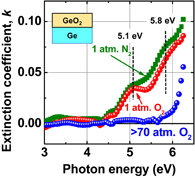
Fig. 18. Extinction coefficient of sputtered GeO2 film on Ge(100) after annealing in N2, 1 atm O2 and HPO at 600 °C, inspected by the spectroscopic ellipsometry. The absorption tail around 5–6 eV appears by annealing in both 1 atm N2 and O2, while no tailing is observed in HPO annealing.23)
Download figure:
Standard image High-resolution imageElectron spin resonance (ESR) studies were also carried out to detect defects in the GeO2/Ge stack.31) Figure 19(a) shows that almost no signals are detected in case of HPO-annealed GeO2 on Ge, while bulk defect signals in other cases are clearly observed. The annealing temperature dependence of defect signals is shown in Fig. 19(b). No magnetic field direction dependence in signals suggests that defects such as the Pb centers commonly observed at SiO2/Si interface are not located at the GeO2/Ge interface. It was also reported that the Pb centers at the GeO2/Ge interface were not detectable by the conventional ESR.48) This too might be again attributed to more flexible bonds in the Ge–O network, although very small Ge dangling bond signals were later detected using electrically detected magnetic resonance (EDMR) measurement.49)

Download figure:
Standard image High-resolution image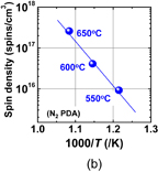
Fig. 19. (a) ESR signals inspected at ∼4.5 K from sputtered GeO2/Ge stack before and after annealing in N2, 1 atm O2 and HPO. (b) Spin density (spins/cm3) in GeO2/Ge stack as a function of annealing temperature in N2-PDA. Defect density increases with increasing annealing temperature. No magnetic field dependence was observed, which means that the observed signals are not from the Pb-center-like interface defects.31)
Download figure:
Standard image High-resolution imageX-ray photoelectron spectroscopy (XPS) analysis has been widely used for characterizing SiO2/Si gate stack properties. Although the sub-oxide analysis has not been established in GeO2/Ge yet, most studies employ the same method for GeO2/Ge as that for SiO2/Si by assuming the Ge4+ position at a given binding energy. The value of Ge4+ is substantially scattered among published reports, so it is presently not safe to evaluate the sub-oxide formation kinetics on Ge by using the same XPS analysis used to evaluate them on Si. It is worthwhile mentioning here that the charging effects50) or the moisture effects51) in the XPS measurement of GeO2 should be much more carefully considered than in the XPS measurement of SiO2/Si. HPO-GeO2 is more robust against the charging in XPS measurement (data not shown).
We systematically measured the band offset at GeO2/Ge by both XPS and internal photoemission (IPE) spectroscopy. The IPE study was carried out in Au (∼15 nm)/GeO2/Ge metal–inulator–semiconductor (MIS) capacitors. IPE can determine the conduction band offset at the oxide/semiconductor interface directly.52) Figure 20 shows our IPE system.53) As shown schematically in Fig. 21, the conduction band offset in HPO-GeO2/Ge was estimated to be 1.65 ± 0.1 eV.54) Furthermore, we observed an appreciable spectrum difference between HPO-GeO2/Ge and APO-GeO2/Ge. In APO-GeO2, there seems to be tailing near the photoemission threshold. This suggests that APO-grown GeO2 may have a huge amount of defect states near the conduction band edge. Smaller values of the energy band gap of GeO2 and band offset at GeO2/Ge reported in the literature might be mainly due to poor GeO2 quality.

Fig. 20. Schematic of the internal photoemission measurement system. The sample was irradiated with a fixed number of photons at each wavelength ranging from 320 to 800 nm.53)
Download figure:
Standard image High-resolution image
Fig. 21. Band diagram of HPO-GeO2/Ge stack estimated from IPE and XPS results. The energy band gap and band offset at GeO2/Ge are about 6 and 1.6 eV, respectively, which are significantly higher than reported. This is because the band tailing states at the interface are efficiently eliminated by the HPO process.54) It can be seen clearly in Fig. 18.
Download figure:
Standard image High-resolution imageAll of the results obtained experimentally show that HPO can produce high-quality GeO2 on Ge in addition to a considerably low Dit. Thus, it is concluded that HPO and HPO+LOA are powerful methods for preparing perfect GeO2/Ge gate stacks without degrading the quality of the GeO2 bulk film or the GeO2/Ge interface. Moreover, it should be emphasized that everything is thermodynamically controlled in the present process.
2.3. Kinetic approach
GeO2/Ge interface formation is always associated with GeO desorption, so HPO is thermodynamically effective for making excellent GeO2/Ge gate stacks. On the other hand, we know that actual reactions are often dominated by kinetics rather than thermodynamics. Therefore, a kinetic suppression of GeO desorption from Ge gate stacks has also been attempted. First, the reaction blocking layer was inserted between GeO2 and Ge. 10-nm-thick GeO2 films were deposited on both Ge and SiO2/Si. Figure 22 shows that the C–V characteristics of a Au/GeO2/Ge MOS capacitor are significantly degraded, while those of a Au/GeO2/SiO2/Si MOS capacitor are apparently normal.22) This suggests that excellent gate stacks on Ge can be obtained by putting a more stable interlayer between Ge and GeO2. If so, GeO2 is no longer needed. In that sense, SiO2/Ge gate stacks might be good.
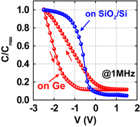
Fig. 22. Bidirectional normalized C–V characteristics of Au/sputtered-GeO2/Ge and Au/sputtered-GeO2/SiO2/Si MIS capacitors in N2-PDA at 600 °C, measured at 1 MHz. GeO2 and SiO2 thicknesses were 10 and 5 nm, respectively. Although the hysteresis observed in the GeO2/Ge stack is scattered from sample to sample, N2-PDA does not degrade gate stacks as long as GeO2 is not in contact with Ge.22)
Download figure:
Standard image High-resolution imageIn fact, a number of efforts using Si-cap technology on Ge have been carried out to achieve good performance of Ge gate stacks, mainly by the IMEC group.55,56) In this method, SiO2/(Si)/Ge is used in place of GeO2/Ge gate stacks. As shown in Fig. 23, Si can be expitaxially grown on Ge in a controlled manner by using a continuous growth process in a chamber,57) although the ultimate control of Si thickness and/or Si oxidation is needed to obtain well-controlled gate stacks. This method has been successfully utilized for Ge MOSFETs57,58) and has made it possible to make use of Si process technology without considering how to suppress the reaction at oxides/Ge. It is a great benefit in the Si cap process on Ge. In our experiments, however, Si passivation works well for Dit in the lower half of Eg but degrades the upper half. This means that it may work for p-MOSFETs but not for n-MOSFETs,59) although our passivation was not by the epitaxial Si growth. Furthermore, from the viewpoints that EOT scaling and narrow process window (whether the Si-cap layer is consumed or not is quite marginal even if the cost issue is not taken into account) and poor electron mobility reasons, we have not employed the Si cap process for Ge gate stack formation.
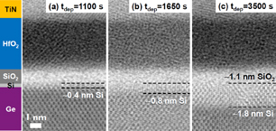
Fig. 23. Cross-sectional TEM images of Si-passivated Ge gate stacks made using various Si deposition times.57) A very thin Si layer epitaxially grown on Ge is observed. Reprinted with permission from Ref. 57. © 2015 IEEE.
Download figure:
Standard image High-resolution imageAnother kinetic approach is the control by cutting the desorption at the top surface instead of suppressing the reaction at the Ge interface in Eq. (2.1). It is expected that a Si cap might serve as a layer blocking GeO desorption from the top. GeO2 films deposited on Ge with and without a Si cap layer were prepared and then annealed in N2 at 600 °C. Figure 24 shows the annealing time dependence in N2 of GeO2 thickness measured by GIXR. With the Si cap, the thickness changes very little with PDA time, while without the Si cap, it decreases with PDA time.59) This suggests that the Si-capped GeO2/Ge MOS capacitor may reveal a very slight degradation in C–V characteristics. To make the Si-cap conductive as the gate electrode, Ni was deposited, followed by silicidation annealing. Figure 25 shows the C–V characteristics of two kinds of GeO2/Ge gate stacks: a GeO2 MOS capacitor annealed in N2 before Au gate electrode deposition, and a MOS capacitor with NiSix-capped GeO2. Well controlled C–V characteristics were achieved only in the latter case.60) This is direct evidence that the kinetic suppression of GeO desorption significantly improves GeO2/Ge gate stacks.
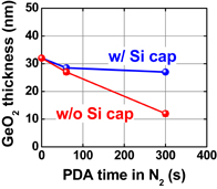
Fig. 24. Thickness reduction of GeO2 film with and without 10-nm-thick Si cap layer on GeO2 in N2-PDA at 600 °C. The Si cap layer can substantially suppress GeO desorption.59)
Download figure:
Standard image High-resolution image
Fig. 25. Bidirectional normalized C–V characteristics of NiSi/GeO2/p-Ge annealed during FUSI gate electrode formation and Au/GeO2/p-Ge annealed before Au deposition. PDA was carried out in N2 for 30 s. In case of FUSI/GeO2, the C–V curve is significantly improved with a small hysteresis, thanks to the suppression of GeO desorption by FUSI capping.60)
Download figure:
Standard image High-resolution imageAlthough we tried to push the kinetic approach forward at the early stage of our Ge research, we have put emphasis on the thermodynamic approach because the metal capping process would be expected to increase the process complexity in device integration. In the material approach discussed in the next section, both the thermodynamic and kinetic approaches are in principle working together. This is a key concept in the EOT scaling discussed in Sect. 4.3.
2.4. Materials approach
From the early stage of our Ge research, we have tried to prepare Ge gate stacks with various high-k dielectrics.61) Our experiences gave us the naïve impression then that trivalent metal oxides such as Y2O3, Sc2O3, and Al2O3 or rare-earth oxides (RE-oxides) might be friendly to Ge in terms of the interface control, while HfO2 should significantly degrade the Ge interface. The results of theoretical calculations also gave us that impression.62)
A difference between Y2O3/Ge and HfO2/Ge is seen in the C–V characteristics in Fig. 26(a).59) More distinctly, the interface quality difference is shown in the Zerbst plot63) in Fig. 26(b). Y2O3 on Ge is much better than HfO2 on Ge from the interface control viewpoint. Figure 27 shows that Y2O3/GeO2 is significantly different from HfO2/SiO2 from the viewpoint of intermixing at the interface.59) In fact, as described later in Sect. 3.1, we achieved the highest electron mobility in Ge MOSFETs with a Y2O3-doped GeO2 (YGO) interface formed by HPO-PDA of Y2O3.58,64) Since Y2O3 or Sc2O3 shows the lowest standard Gibbs free energy change (ΔG°) among various oxides thermodynamically, Y or Sc diffusion to GeO2 enables the GeO desorption to be suppressed very effectively. This is discussed in more detail in Sects. 4.2 and 5.2 from the viewpoints of both oxygen potential control and gate stack reliability. Thus, in our experience, we have come to the conclusion that YGO should be a most promising gate dielectric film on Ge. In terms of the EOT scalability, however, YGO can be the interlayer between a real high-k material and Ge because the dielectric constant of YGO is not so high (k = 6–8). This is discussed in Sect. 4.2.

Download figure:
Standard image High-resolution image
Fig. 26. (a) Bidirectional C–V characteristics of Au/Y2O3/p-Ge and Au/HfO2/p-Ge capacitors annealed at 400 and 600 °C in N2 for 30 s. (b) Zerbst plots for Au/HfO2/p-Ge and Au/Y2O3/p-Ge MIS capacitors annealed at 600 °C in N2, deduced from the transient capacitance measurements with Vg = 2 V at 120 K. The Y2O3/Ge interface is much better than the HfO2/Ge one in terms of the minority carrier generation time.59)
Download figure:
Standard image High-resolution image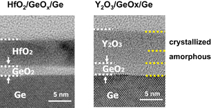
Fig. 27. Cross-sectional TEM images of HfO2/GeO2/Ge and Y2O3/GeO2/Ge stacks after annealing at 600 °C in N2. The bottom part of Y2O3 is not crystallized, while all parts of HfO2 are crystallized. Y2O3 is more easily mixed with GeO2 than HfO2.59)
Download figure:
Standard image High-resolution imageIt is practically feasible to use Al2O3 for Ge gate stacks. The Al2O3/GeOx/Ge gate stacks have been intensively studied.65,66) In this process, atomic layer deposition (ALD)-Al2O3 was deposited and the deposition was followed by plasma-excited O* PDA at 300 °C. In fact, Al2O3 is most easily deposited by ALD. The cross-sectional view and TEM image are shown in Figs. 28(a) and 28(b), respectively.66) Takagi's group further reported that the interface GeOx formation was needed to keep the low Dit shown in Fig. 28(c).65) 1-nm-thick GeOx is needed to achieve a low Dit, and the interface is degraded when the thickness is about 0.5-nm-thick GeOx. A good point of this process is that the Al2O3 layer works as a plasma-protection barrier and an oxygen-diffusion stopper in addition to being friendly to the conventional CMOS process.

Download figure:
Standard image High-resolution image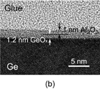
Download figure:
Standard image High-resolution image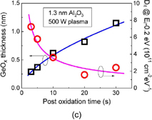
Fig. 28. Al2O3/GeOx/Ge gate stacks proposed by Takagi's group. (a) Schematic image of fabricated Ge MOSFET. (b) Cross-sectional TEM image of Al2O3/GeOx/Ge gate stack. (c) GeOx interface layer thickness formed by the ECR plasma post oxidation through 1.3-nm-thick Al2O3 and Dit of Au/Al2O3/GeOx/Ge MOS capacitor as a function of the post oxidation time. Below 1-nm-thick GeOx, Dit increases significantly.66) Reprinted with permission from Ref. 66. © 2012 IEEE.
Download figure:
Standard image High-resolution imageSince we think that Al-strengthened GeO2 might be formed at the interface, it is in some sense similar to the YGO interface proposed above. Namely, both YGO and Al2O3-doped GeO2 can serve as an oxygen-diffusion-blocking layer and stabilize GeO2 by forming the film with modified continuous random network. This is the kinetic control of Ge gate stacks. From this viewpoint, the material approach of selecting the right material requires consideration of the thermodynamic as well as kinetic control of GeO2 on Ge. Both of them are crucially important for establishing reliable ultrathin-EOT gate stacks and so are discussed in Sect. 5.2.
Another material approach is from the rare earth oxides on Ge. Figure 29(a) shows C–V characteristics of a Ge MOS capacitor prepared by HPO of (La–Lu)2O3 (LLO). They look almost ideal.67) It is interesting to note that LLO is a real high-k material (k ∼ 20) and stays amorphous up to around 1000 °C.68) As shown by the TEM image in Fig. 29(b), a rather thick interface layer was formed by HPO. We noted that the interface layer was not pure GeO2 but LLO-mixed GeO2.69) Since we have not optimized the LLO gate stack, we will no longer talk about it in this paper. However, further optimization might make it a great gate stack on Ge.

Download figure:
Standard image High-resolution image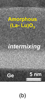
Fig. 29. (a) Bidirectional C–V characteristics of (La–Lu)2O3/Ge annealed in HPO at 600 °C. The ratio of La to Lu is ∼1 in this case. (b) Cross-sectional TEM image of HPO (La–Lu)2O3/Ge stack. The C–V curve looks ideal, while a thick amorphous interface layer is grown between (La–Lu)2O3 and the Ge substrate.67)
Download figure:
Standard image High-resolution imageAt the early stage of considering Ge compounds on Ge, GeON instead of pure GeO2 was favorably considered in analogy to SiON in advanced Si technology.70–76) C–V characteristics were much improved, but a high-electron-mobility benefit in Ge n-channel FETs has not so far been reported. We paid attention to the fact that N could also lower the oxygen potential thermodynamically as discussed later in Sect. 3.3.77,78) So GeO desorption could be reduced and the interface properties might be improved by fine-tuning the N profile in GeO2. As we did not have an appropriate technique for the optimum nitridation of Ge for N not to be located at the interface, we stopped studying the GeON gate stack. But it has a potential for the further improving the interface layer.
2.5. Oxidation kinetics of Ge
Ge oxidation at an optimized temperature is obviously the most popular method to form Ge gate stacks, as it is to form Si gate stacks. To suppress GeO desorption, low-temperature oxidation is thermodynamically favored. Matsubara et al. showed that C–V characteristics with a relatively low Dit could be obtained by just oxidizing Ge at 550 °C.79) Although that seems to be inconsistent with our results, we cannot say that there is no process window for improving gate stack characteristics just by a simple oxidation. Nevertheless, even if there might be such a small process window, GeO2 becomes thermodynamically unstable at rather high temperatures above 600 °C.
Although so far we have mainly discussed GeO desorption from GeO2/Ge gate stacks, we actually need to understand Ge oxidation kinetics. As mentioned previously, the oxidation rate of Ge is described by the linear-parabolic law like that describing the oxidation rate of Si. Although as mentioned in Sect. 2.2.2, Ge oxidation appears so related to the GeO desorption process, it is not obvious whether the Deal–Grove model is or is not valid for Ge. Two experimental results that cannot be easily explained by the Deal–Grove model are discussed in the following.
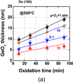
First, the anomalous p-O2 dependence of the rate of Ge oxidation is discussed. Ge(100) wafers were oxidized in wide ranges of temperature and p-O2. GeO2 thickness versus oxidation time at 500 °C is shown in Fig. 30(a) with of p-O2 as a parameter. GeO2 thickness versus p-O2 temperature is shown in Fig. 30(b) with the oxidation temperature as a parameter.80) Note a reverse p-O2 dependence of the oxidation rate. It is surprising that the oxidation rate is reduced below 520 °C as the p-O2 increases above a critical p-O2. This has never been observed in the oxidation of Si. It is hereafter called low-temperature high-pressure O2 (LT-HPO) oxidation. It is strange because a higher p-O2 means a larger amount of O2 molecules in the ambient. Note that in Fig. 30 p-O2 is denoted by the room-temperature p-O2. Anomalous p-O2 dependence in low p-O2 was also discussed in Ref. 21. Therefore, it is general behavior in Ge oxidation, depending on the temperature. Figure 31 shows that (a) the density of LT-HPO GeO2, estimated by GIXR, is greater than that of HT-HPO GeO2 and (b) the wet etching rate is significantly reduced in LT-HPO. This suggests that the reverse p-O2 dependence may be partly due to the densification of the GeO2 film. We applied the Deal–Grove model to characterize the results. To qualitatively reproduce the experimental behavior shown in Fig. 30, improbably large pressure–dependent B parameter in the Deal–Grove equation is needed as shown in Fig. 32.
Download figure:
Standard image High-resolution image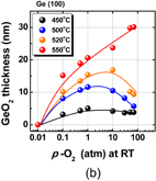
Fig. 30. (a) Oxidation time dependence of GeO2 thickness on Ge(100) at 500 °C at various p-O2 values. (b) GeO2 thickness vs p-O2 relationship at various oxidation temperatures, where oxidation time was fixed for 30 min. A reverse p-O2 dependence of the oxidation rate below 520 °C appears around atmospheric p-O2.80) Such characteristics have never been observed in Si oxidation, to the best of our knowledge. Note that, here, p-O2 is the O2 pressure at room temperature before increasing the temperature.
Download figure:
Standard image High-resolution image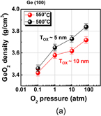
Download figure:
Standard image High-resolution image
Fig. 31. (a) Density of GeO2 films grown at 500 and 550 °C as a function of p-O2 estimated by GIXR. It increases with increasing p-O2. (b) Thicknesses of LT-HPO- and APO-grown GeO2 films as a function of wet etching time. Thickness was estimated by XPS. The wet etchant was methanol-diluted water (methanol 100 cm3, H2O 5 cm3). The LT-HPO-grown GeO2 exhibits denser characteristics than the APO-grown one.80)
Download figure:
Standard image High-resolution image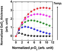
Fig. 32. Calculated relationship between GeO2 thickness and p-O2 with normalized oxidation temperature as a parameter. This was calculated using a simple oxidation model with a large pressure–dependent B parameter in the Deal–Grove linear parabolic law.80)
Download figure:
Standard image High-resolution imageTo understand the Ge oxidation correctly, the oxygen atom kinetics should be clarified, since we know that the oxygen atoms diffuse much more easily than Ge in GeO2, as discussed in Fig. 8. In order to trace the oxygen atom movement in the oxidation, the isotope 18O marker experiment was carried out. A Ge16O2 (∼10 nm)/Ge sample grown conventionally was reoxidized by 18O2, and then both 18O and 16O profiles in the film were inspected by the high-resolution Rutherford backscattering spectrometry. The results showed that 18O was not localized at the GeO2/Ge interface but spread throughout the film.81) This is in contrast with the Deal–Grove model commonly recognized for Si. In order to more clearly confirm the oxidation kinetics of Ge, both Ge16O2/Ge and Si16O2/Si samples have recently been prepared again by the normal 16O2 oxidation of Ge and Si substrates, at 550 °C for GeO2/Ge and at 900 °C for SiO2/Si (the temperatures are equivalent to each other when normalized by the melting temperature). The initial thickness was relatively thick (∼120 nm) for both GeO2 and SiO2. Then both were put into a 100% (actually above 98%) 1 atm 18O2 ambient, as shown in Fig. 33(a). The oxide thickness was increased to about 130 nm for both cases. These samples were inspected by the SIMS measurement. The depth profiles of secondary ion intensity of both 18O and 16O are shown for GeO2/Ge and SiO2/Si systems in Fig. 33(b).82) Look at the profile difference of 18O at the Ge interface from that at the Si one. 18O is accumulated at the interface in the Si case, which was as reported previously,83) while in the GeO2/Ge case, 18O gradually decreases to the interface. Since the Deal–Grove model predicts that the oxide is newly formed through the reaction of O2 with semiconductors at the interface, 18O accumulation should be observed as in the Si case. The fact that no special feature at the interface was observed definitely indicates that the Deal–Grove model is not applicable to Ge oxidation.
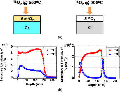
Fig. 33. (a) Schematic images of samples to trace the 18O atom movement in oxidation process at 550 and at 900 °C in Ge and Si, respectively. (b) Depth profile measured by SIMS of 18O/(18O + 16O) in Si16O2/Si and Ge16O2/Ge stacks after additional 18O2 oxidation. In case of Si, 18O is predominantly detected close to the surface and at the SiO2/Si interface, whereas in case of GeO2/Ge, it is not observed at the interface but is detected almost uniformly (gradually decreasing toward the interface) in the film. This result indicates that Ge oxidation cannot be described by the simple Deal–Grove model.82)
Download figure:
Standard image High-resolution imageWhat is the possible kinetics of Ge oxidation over the Deal–Grove model? Although it is still under investigation, our view is roughly described as follows.82) In case of Ge oxidation, we should take account of GeO desorption, in which Vo diffusion is involved. In fact, a work reported in a recent paper found that the oxygen vacancy Vo may be involved in the oxidation process by inspecting the nuclear reaction profiling of 18O.84) The SIMS results in Fig. 33 also suggest that O atoms should diffuse through the GeO2 film. It is unsure whether this is driven by an exchange process like that discussed in GeO desorption in Sect. 2.1, with the help of Vo formation, or by the interstitial-mediated diffusion.85) The Vo-mediated model, however, seems to be reasonable when it is considered that HPO can suppress Vo generation inside the film thermodynamically, resulting in the significant suppression of the oxidation shown in Fig. 30. Namely, the oxidation of Ge is likely to be driven by the Vo generation at the interface in Eq. (2.4), followed by the reaction between Vo and O. The analytical model like the Deal–Grove one is now under way to establish.
Finally, ozone or O* (oxygen radical) oxidation of Ge is briefly discussed. It was investigated particularly by a group at Stanford University,86) in order to suppress partly GeO desorption by employing a low-temperature process. Ge can be oxidized by ozone or O* at low temperatures with a quite low activation energy, thanks to the high oxidation power of ozone or O*. In the ozone or O* oxidation process, the lifetime of O* concentration, which is dependent on the temperature, should be taken into account. Therefore, the simple Deal–Grove model is not applicable even for the Si case. We studied the O* oxidation of Ge by using O*, which was generated by the µ-wave excited plasma (2.45 GHz) as shown in Fig. 34.87) A distinct difference between normal O2 (including HPO) and O* oxidation is that, as shown in Figs. 35(a) and 35(b), there is little temperature dependence in O* oxidation. C–V characteristics were good, particularly for thin GeO2 formation. However, we stopped the O* process research because the films were not stable at higher temperatures. It may be resumed when the low-temperature oxidation is definitely needed.
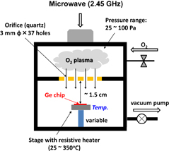
Fig. 34. Schematic image of the radical oxidation system used in our experiment. O* was excited by 2.45 GHz microwave. The oxidation space was separated from the O2 plasma space through small quartz orifices.87)
Download figure:
Standard image High-resolution image
Download figure:
Standard image High-resolution image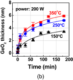
Fig. 35. Thickness of GeO2 grown by the radical oxidation with the power of (a) 100 and (b) 200 W at various temperatures as a function of oxidation time. Even at low temperatures, Ge was oxidized by O*. The activation energy of O* oxidation was very small (∼0.1 eV).87)
Download figure:
Standard image High-resolution image3. Enhancing electron mobility in Ge MOSFETs
The carrier mobility is one of the most important device properties even in the ballistic transport regime. We, however, will not discuss the Ion/Ioff ratio by fabricating ultra short-channel FETs in this paper. Nevertheless, since the carrier mobility is very sensitive to the interface properties, it is a quality indicator of the carrier transport at the interface. Therefore, intrinsic scattering mechanisms are only discussed in the framework of the Matthiessen's rule. Let us start with the Coulomb scattering discussion first.
3.1. Dit reduction
We are interested in Ge CMOS, but as mentioned in the introduction, so far, n-MOSFET technology has actually been a bottleneck. Therefore, it is a big concern that n-channel Ge MOSFETs might be intrinsically poor even though the bulk electron mobility is expected to be high.88) We applied the gate stack formation process described in the previous sections to n-MOSFET fabrication. Long-channel n-MOSFETs were fabricated on a Ge substrate using the two-step HPO+LOA process.38) Several channel lengths (W/L = 90 µm/100–500 µm) were defined, and phosphorus (1 × 10¹⁵/cm2 dose) was implanted with 100 keV to form source/drain (S/D) regions. Such large FETs enabled us to estimate electron mobility very accurately using the split C–V technique without being worried about by size uncertainty and/or parasitic resistance and capacitance. GeO2 was grown at 550 °C for 10 min in HPO (p-O2 = 70 atm at room temperature), followed by LOA at 400 °C. Then, Al was deposited and defined for the gate electrode. Note that spacer Y2O3 was used to protect GeO2 from the wet process and air exposure because we found that Y2O3 was water-resistant and rather compatible with Ge as discussed in Sect. 2.4.
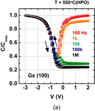
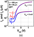
Figure 36(a) shows the transfer characteristics (IS–VG) of Ge(100) n-MOSFETs in which GeO2 was grown by HPO+LOA.38) The Ion/Ioff current ratio at 300 K was about ∼104. The subthreshold swing (S-factor) was 125 mV/dec, which was rather high, considering the low Dit determined using the conductance method (Fig. 14). Since the S-factor should have a linear temperature dependence around room temperature,89) the temperature dependence of the S-factor was measured from 150 to 300 K, as shown in Fig. 36(b). The S-factor at 300 K extrapolated from the temperature dependence was 95 mV/dec,39) which was reasonable and much smaller than the measured value. This suggests that the S-factor at 300 K might be degraded owing to the S/D junction leakage current in the subthreshold region in this device. The impact of LOA on the electron effective mobility (μeff) in addition to that of HPO is shown in Fig. 37 as a function of electron density. On Ge(100), the peak electron mobility after HPO+LOA was 810 cm2 V−1 s−1, while that after HPO was 610 cm2 V−1 s−1. The lower μeff in MOSFET fabricated by HPO only is explainable by the Coulomb scattering due to relatively high values of Dit (Fig. 12).
Download figure:
Standard image High-resolution image
Fig. 36. (a) Transfer characteristics of Ge(100) n-MOSFET with a gate stack grown by HPO+LOA at VDS = 5 mV and 1 V. Both ID and IS are shown. (b) Temperature dependence of S-factor (SS) from 150 to 300 K. The S-factor estimated from a linear extrapolation to 300 K is ∼95 mV/dec, which is much smaller than the measured one. This difference may come from the S/D junction leakage current.39)
Download figure:
Standard image High-resolution image
Fig. 37. Effective electron mobility as a function of inversion electron density (Ns) in MOSFETs with GeO2 grown both by HPO and HPO+LOA. The peak electron mobility in a GeO2/Ge gate stack grown by HPO+LOA was about 800 cm2 V−1 s−1. By adding LOA, the effective mobility was improved particularly at low electron densities.39) The mobility was estimated by the split C–V method.
Download figure:
Standard image High-resolution image3.2. Substrate surface orientation
As already mentioned in Sect. 2.2, the surface orientation of Ge substrates affects both the GeO2 formation and GeO desorption processes. In this section, we discuss the effect of substrate surface orientation on electron mobility. Figure 38 shows that the peak electron effective mobility on Ge(111) was about 1,100 cm2 V−1 s−1 at 300 K and was 1.4 times better than that of Ge(100).39) This suggests that the (111) surface should intrinsically be better than the (100) one not only with regard to the process stability as discussed in Sect. 2.2 but also with regard to the FET performance. An advantage of MOSFETs on the Ge(111) surface under the ballistic carrier transport was expected from the analytical estimation of two-dimensional projections in the conduction-band energy.90) The (100) surface in Si, roughly speaking, corresponds to the (111) surface in Ge as shown in Fig. 39. This view is also applicable for the diffusive transport case in terms of the effective mass. In actual scaled CMOS design, the surface orientation effects are discussed in conjunction with strain effects in both Si and Ge.91) In particular, a possible method to make the best of strain effects on the mobility in Fin-FETs is now deliberately studied both experimentally and theoretically,92,93) as obviously expected from two-dimensional projection views. In this review, however, we would focus on unstrained transport characteristics to pay attention to the material and process fundamentals of Ge.

Fig. 38. Substrate orientation dependence of electron mobility in Ge n-MOSFETs with HPO+LOA GeO2 gate stack. The peak electron mobility of 1100 cm2 V−1 s−1 was 1.4 times higher on Ge(111) than that on Ge(100). Note that both values are above the Si universal mobility shown by the solid line. This is the direct observation that Ge(111) has high potential for enhancing the FET performance for the first time.39)
Download figure:
Standard image High-resolution image
Fig. 39. Conduction-band energy minima and their projections on (111) and (100) for Ge and Si. Ge(111) is expected to be better than Ge(100) in terms of the lower electron effective mass in the two-dimensional inversion layer. This is in contrast to the Si case.
Download figure:
Standard image High-resolution imageWe further improved the electron μeff by optimizing the two-step HPO+LOA process for Y2O3 on Ge(111). Figure 40 shows the peak electron mobility progress with the calendar year.31) The peak electron and hole mobility values obtained so far have approached 1,920 cm2 V−1 s−1 on Ge(111) and 720 cm2 V−1 s−1 on Ge(100). The highest electron mobility case is for Y2O3 on Ge(111) by using the HPO+LOA process with a longer LOA time. It is about ×2.5 of the universal electron mobility in Si MOSFETs and about half of the bulk electron mobility in Ge. Note that, as discussed in Sect. 2.4, the interface of this gate stack is YGO rather than Y2O3. This interface may further decrease Dit, resulting in the peak electron mobility enhancement. Concerning the hole mobility, we have also improved it to ×3.5 that of Si without any strain effect. These results certainly encourage us to promote Ge CMOS. Figure 41 shows the μeff values of electron and hole as functions of electron and hole densities, with different LOA times and different surface orientations of Ge.64)
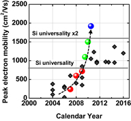
Fig. 40. Peak electron mobility progress in planar Ge n-MOSFETs with the calendar year. Mobility values reported in the literature are shown by gray diamonds, while our data are shown by colored solid circles.31) The present peak electron mobility in Ge n-MOSFET is higher than twofold the Si one.
Download figure:
Standard image High-resolution image
Fig. 41. Effective hole and electron mobilities in Ge p- and n-MOSFETs as a function of carrier density. The highest hole mobility of 725 cm2 V−1 s−1 is roughly 3.5 times higher than Si universal one, and the highest electron mobility of 1920 cm2 V−1 s−1 is a record-high value in Ge n-MOSFETs. With an increase in LOA time, the peak electron mobility is improved.64)
Download figure:
Standard image High-resolution imageIn the conventional mobility analysis, the temperature dependence is the property best characterizing the scattering mechanism in the channel.94) The temperature dependence of the peak electron μeff is shown in Fig. 42, where the slope of temperature dependence changes from positive to negative with an increase in the peak electron μeff. This clearly suggests that the scattering mechanism changes from Coulomb to phonon scattering. Namely, the electron transport in the inversion channel has become intrinsic with dramatic interface improvements. To our knowledge, this is the first demonstration of phonon scattering limited mobility in Ge n-MOSFETs.
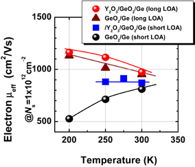
Fig. 42. Temperature dependence of electron mobility at Ns = 1 × 10¹²/cm2. The increase in electron mobility with decreasing the measurement temperature indicates that phonon scattering dominates the electron mobility in the best case with the long LOA time, while the Coulomb scattering degrades the electron mobility with the short LOA time. The importance of LOA should be emphasized from the viewpoint of suppressing the Coulomb scattering.64)
Download figure:
Standard image High-resolution imageEverything so far seems to be good. What is the remaining problem? Concerning the carrier mobility, it has often been claimed that the most relevant mobility in the actual circuit operation is not the peak mobility but that in the high-electron-density region. That is absolutely true. The electron mobility in high Ns region in Fig. 41 is almost comparable to that of the Si counterpart. Does this mean that there is no future for Ge CMOS? In the next section, we focus on this. Another concern is the mobility reduction in the thin EOT region.55) This is actually very important in CMOS scaling and will be discussed in Sect. 4.
3.3. Atomically flat Ge surface
As shown schematically in Fig. 43, Coulomb scattering, phonon scattering, and surface roughness scattering are widely recognized as dominant carrier scattering mechanisms in the Si inversion channel.91) By employing HPO in the Ge oxidation, Coulomb scattering has been dramatically reduced, thanks to the Dit reduction, resulting in the peak electron mobility in Ge now being 2.5 times that in Si. Reasoning by analogy to the Si MOSFET, one may suspect that the larger surface roughness on Ge might degrade the mobility at high electron density (high effective field, Eeff). However, we reported that the rms value measured by the AFM was not necessarily related to the high-Ns electron mobility.95) Here, note that not only the roughness height but also the roughness correlation length should be considered in the conventional roughness scattering formulation.96) We therefore tried to realize the atomically flat surface on Ge in order to achieve both ultimately small rms and large correlation length in the surface roughness.
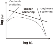
Fig. 43. Schematic of dominant carrier scattering mechanisms in the Si MOS inversion layer. Three mechanisms such as Coulomb, phonon, and surface roughness scatterings are generally considered in the carrier transport in Si MOSFETs. By using the Matthiessen's rule, the carrier mobility is described by the broken line.
Download figure:
Standard image High-resolution imageWe fortunately succeeded in preparing the atomically flat surface by H2 annealing.97) This method has been widely used on Si surfaces,98) but to our knowledge, this was its first demonstration on Ge. Figure 44(a) shows an AFM image of the Ge(111) surface in H2 annealing at 650 °C, in which only a couple of atomic steps are clearly observed in an area ∼1 µm square. Each step corresponds to one monolayer on Ge(111), as shown in Fig. 44(b). As shown in Fig. 45, this H2 annealing method also enabled atomically flat surfaces on Ge(110) and (100) to be formed at relatively high temperatures.99) Although the surface planarization mechanism has not been studied in detail, microscopic surface patterns on three surfaces on Ge are the same as those on Si, and the same kinetics that work for Si may work for Ge as well.
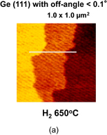
Download figure:
Standard image High-resolution image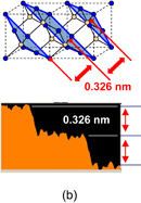
Fig. 44. (a) AFM image of Ge(111) surface after annealing in 1 atm H2 at 650 °C. A clear step-and-terrace structure is observed in an area of 1 × 1 µm2. (b) Cross-sectional height profile at the line shown in (a). It clearly shows the 0.326 nm height of a single step on the Ge(111) surface.97)
Download figure:
Standard image High-resolution image
Download figure:
Standard image High-resolution image
Fig. 45. AFM images of (a) Ge(110) and (b) Ge(100) surfaces on 1 × 1 µm2 in H2 annealing at 550 and 850 °C, respectively. Step-and-terrace structures are clearly observed on both surfaces as well.99)
Download figure:
Standard image High-resolution imageNote here that what is needed is not an atomically flat surface but an atomically flat interface with a dielectric film after the gate stack formation. To investigate how the atomically flat surface was affected by the oxidation process, the atomically flat Ge(111) surface was oxidized in HPO (∼5 nm) at 500 °C. AFM images before and after oxidation are shown in Fig. 46(a). It is surprising that the step-and-terrace structures are clearly maintained in the oxidation. Figure 46(b) summarizes systematic results of the rms roughness after the oxidation when the temperature and p-O2 were changed.100) The roughening is by and large suppressed at lower temperatures under high p-O2, in which atomically flat interface is maintained. The fact that LT-HPO actually keeps the interface flat was also observed on as-cleaned Ge surfaces. Figure 47 shows the rms histogram at 500 °C with p-O2 as a parameter. A decrease in the histogram width on the as-cleaned Ge surface means that the oxidation under higher p-O2 at 500 °C can reduce the surface roughness. The roughening process should be directly associated with the oxidation of the Ge substrate and will be further discussed in Sect. 4.
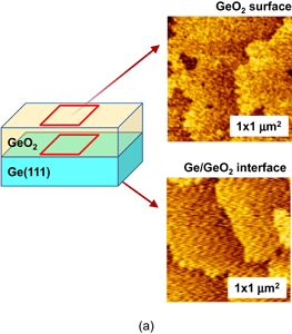
Download figure:
Standard image High-resolution image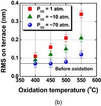
Fig. 46. (a) AFM images of GeO2 surface and GeO2/Ge(111) interface after oxidation at 500 °C in 70 atm p-O2. The large step-and-terrace structure is clearly observed on both the GeO2 surface and the GeO2/Ge interface even after 5-nm-thick GeO2 growth. For the interface observation, GeO2 was removed with deionized water. (b) The rms roughness on a single Ge terrace as a function of oxidation temperature. Values are shown for GeO2 thickness of about 5 nm for three p-O2 values. The AFM measurements were performed in 0.3 × 0.3 µm2. The atomically flat surface is likely to be maintained by and large at lower temperatures and at high p-O2.100) The minimum rms obtained in the experiments is limited by our AFM resolution.
Download figure:
Standard image High-resolution image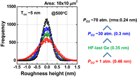
Fig. 47. Roughness height histogram of as-cleaned Ge surface and oxidized interfaces at 500 °C in various p-O2 values. Thermally grown GeO2 was removed with deionized water before AFM measurement. The flat surface is obtained by carrying out the oxidation at high p-O2.100)
Download figure:
Standard image High-resolution imageLet us go back to the effect of surface flatness on electrical properties. Figure 48 shows the μeff–Ns relationship in three kinds of processed FETs.101) FET-A was fabricated on the atomically flat Ge(111) by HPO at 500 °C, FET-B was fabricated by HPO at 500 °C, and FET-C was fabricated by HPO at 550 °C. The peak electron mobility is almost the same for each of the samples because of the very low Dit at the GeO2/Ge interface, while the high-Ns electron mobility of each is distinctly different from those of the others. Only FET-A shows significantly higher electron mobility in the high-Ns region. Thus, it is concluded that the surface roughness control followed by the appropriate oxidation enables us to improve the high-Ns electron mobility. Concerning the poor electron mobility in the high-Ns region, another possible origin is that there might be more interface defects near the conduction band edge of Ge.102) This is partly true because the surface planarization might reduce such ionized defects as well, while it is also true that the Coulomb scattering may be reduced, thanks to the more effective screening by free carriers present at high densities. The border traps in dielectric films with poor interface on Ge or the real space transfer of electrons from the channel to the dielectric film side (carrier spillover effect) may also be a concern in case of the low energy barrier at the Ge interface. Although further analysis is obviously needed, the facts that atomically flat surface planarization of the Ge substrate by H2 annealing definitely improves the high-Ns electron mobility and that a good Ge interface with HPO cannot solve the mobility degradation at the high-Ns region suggest that the degradation origin should exist in the Ge substrate side including the surface. Whatever the H2 annealing effect mechanism is, this is good news from the technical perspective.
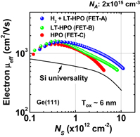
Fig. 48. Electron mobility in Ge(111) n-MOSFET as a function of inversion electron density (Ns). Note that high-Ns electron mobility is much improved, thanks to Ge interface planarization by both H2 annealing and layer-by-layer oxidation in LT-HPO, while the peak mobility does not change very much. It shows that high-Ns electron mobility is sensitive to the interface roughness, as expected.101) Nevertheless, since it is also possible that the surface roughness might induce the interface defects and/or additional interface charges rather than generating the roughness potential, a new theoretical framework of the scattering mechanism may be further needed.
Download figure:
Standard image High-resolution image3.4. Defects in Ge substrate
The electron mobility in Ge MOSFETs has been enhanced remarkably thanks to the significant reduction of carrier scattering origins such as Dit and the surface roughness. Concerning a single FET, the channel interface in the Ge gate stack is obviously crucial for improving the carrier transport in the channel, while the Ge substrate has not been seriously considered because phonon scattering should be "intrinsic" in Ge. In this section, we discuss that the substrate can affect the electron mobility even when device fabrication processes are exactly the same.103) We prepared Ge MOSFETs on two different kinds of p-Ge wafers, denoted here by wafers A and B. Both gate stacks were formed by HPO-GeO2 as described previously. Figure 49 shows the effective electron mobility as a function of electron density on two kinds of wafers. Note that there is a striking difference in the effective electron mobility at the low-electron-density region. According to the conventional analysis of the inversion layer mobility in Si-MOSFETs, the Coulomb scattering probability should be quite different between two kinds of MOSFETs on wafers A and B. There are two sources of Coulomb scattering centers in Ge gate stacks. One is at the GeO2/Ge interface and/or in GeO2, and the other is in the Ge bulk. Figure 50 shows Dit spectra of two gate stacks on wafers A and B, estimated by the low-temperature conductance method.101) No difference in Dit spectra is observed between them. Furthermore, the dopant density was almost the same in the SIMS measurement. This suggests that the probabilities of Coulomb scattering by Dit and dopant atoms should be the same between A and B. Thus, the significant mobility degradation on wafer B in Fig. 49 seems mysterious in the conventional scattering analysis in FETs.
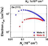
Fig. 49. Electron mobility in Ge(111) n-MOSFETs fabricated on two kinds of differently grown Ge wafers (wafers A and B). Despite the same process steps used in their FET fabrication, their mobilities differ significantly. This indicates that an additional scattering mechanism should be involved in Ge n-FET channels.101)
Download figure:
Standard image High-resolution image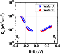
Fig. 50. Comparison of the energy distribution of Dit (estimated by low-temperature conductance method) in (HPO+LOA) GeO2/Ge stacks fabricated on wafers A and B. No difference is observed at the interfaces on different wafers, although a significant difference is observed in the effective mobility.101)
Download figure:
Standard image High-resolution imageAs discussed in Sect. 3.3, H2 annealing is effective for achieving an atomically flat surface of Ge substrates. Together with this finding, we found that the H2 annealing of wafer B could improve the electron mobility significantly as shown in Fig. 51.103) Increasing the H2 annealing temperature enhances the peak electron mobility significantly. In addition, it is interesting to see that the H2 annealing of Ge wafer B does not affect the hole mobility in p-channel Ge MOSFETs. The results suggest that possible defects seem to be electrically inactive in the accumulation and depletion regions of the p-Ge substrate. Also note that, as shown in Fig. 52, Dit is not at all sensitive to H2 annealing, as expected from Fig. 50. This suggests that there may be a new origin of the electron mobility degradation in the Ge substrate, because the peak electron mobility is not affected very much by the surface roughness scattering. Here, we note that the oxygen concentration near the surface of wafer B is reduced in H2 annealing and depends on the annealing temperature as shown in Fig. 53. In wafer A there was no oxygen detectable by the SIMS. Typical metals in wafer B were not present at levels above 5 × 10¹⁰ atoms/cm2.
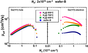
Fig. 51. Impact of H2 annealing on effective mobility in MOSFETs fabricated on wafer B. Electron mobility is much improved by annealing in H2 at higher temperatures.103) Note that the surface flatness was the same for both wafers in H2 annealing (data not shown). Interestingly, hole mobility is not affected much between wafers A and B.
Download figure:
Standard image High-resolution image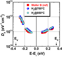
Fig. 52. Comparison of the energy distribution of Dit in (HPO+LOA) GeO2/Ge stacks fabricated on wafer B annealed in H2 at 700 and 850 °C. No difference in Dit at the interface is observed on wafers differently annealed in H2.103)
Download figure:
Standard image High-resolution image
Fig. 53. Depth profile of oxygen in Ge wafer B measured by SIMS, in H2 annealing at 700 and 850 °C. The oxygen concentration close to the Ge surface is reduced significantly by increasing the H2 annealing temperature.103)
Download figure:
Standard image High-resolution imageTo further investigate the oxygen effects, oxygen ions (100 keV, 1013 cm−2) were intentionally implanted in wafer A, as indicated in Fig. 54(a). Figure 54(b) shows that the electron mobility is significantly improved by H2 annealing.103) In fact, as shown in Fig. 55, the oxygen profile in wafer A differed significantly between the conditions with and without implanted oxygen.101) Note that the step-and-terrace structure of the Ge surface was exactly the same for both wafers A and B. Hence, the oxygen-related scattering centers in the Ge wafer could be the origin of electron mobility degradation in Ge n-MOSFETs.
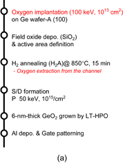
Download figure:
Standard image High-resolution image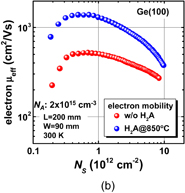
Fig. 54. Impact of the oxygen implantation into wafer A followed by H2 annealing on effective electron mobility. The process steps are described in (a). (b) Electron mobility is degraded by the oxygen implantation, but is surprisingly restored almost to its initial mobility by H2 annealing (H2A).103)
Download figure:
Standard image High-resolution image
Fig. 55. Oxygen profile in Ge(100) wafer A with and without oxygen ion implantation (1013 cm−2). The oxygen concentration in wafer A was originally below the detection limit (near 1015 cm−3) of the SIMS measurement.101) The profile near the surface is mainly due to artifacts in the SIMS measurement, because no difference of oxygen concentration near the surface between w/ and w/o oxygen is observed.
Download figure:
Standard image High-resolution imagePossible defects in the inversion state are schematically depicted in Fig. 56, in which the defect might be an acceptor type and located in the upper half of the energy band gap.103) Although the DLTS measurement was carried out to characterize oxygen-related defects in wafer B, no difference has been observed.104) The exact origin is still under investigation, but this finding points out that the oxygen control in the Ge substrate is substantially important for achieving high-performance Ge n-MOSFETs. The Ge wafer quality has not matured yet, which means that there is plenty of room to optimize it. Note that the above considerations should be applied not only for Ge wafers but also for epitaxially grown Ge films.
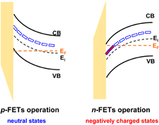
Fig. 56. Schematics of possible oxygen-related scattering centers in Ge substrate for effective electron and hole mobilities in MOSFETs. It is inferred that the neutral states (which might work as electron scattering centers) induced by dissolved oxygen may exist in the upper half of the energy band gap in Ge because it is possible for defects to be negatively charged at the inversion state in n-MOSFETs. In p-MOSFETs, those defects may not work as scattering centers.103)
Download figure:
Standard image High-resolution image4. Scaling EOT
To operate miniaturized FETs successfully, a number of challenges obviously have to be met. The short-channel effects such as DIBL and the leakage current such as GIDL will be in principle severer in Ge because of its higher dielectric constant and narrower energy band gap, respectively. Multi-gate structures (including FinFETs) will be helpful for enhancing the gate controllability in short-channel FETs. Thin-channel FETs are also beneficial from the viewpoint of junction leakage current reduction, which is discussed in Sect. 7. In any case, a thinner EOT has been generally the most powerful way of making short-channel FETs viable. It is, however, quite challenging for us because HPO is naturally expected to form thicker GeO2 even though the GeO2/Ge interface is surprisingly good. This was a big hurdle on our GeO2/Ge FETs and brought unfavorable comments concerning HPO-GeO2. Furthermore, realizing nanometer-level FETs will definitely require the use of high-k materials on Ge. Thus, it is mandatory and urgent to develop ways to make thinner EOT gate dielectrics on Ge while keeping their quality high.
4.1. Low-temperature high-pressure O2 oxidation
We have already discussed the LT-HPO, which enables thin GeO2 to be formed on Ge by the thermal oxidation process under a high O2 pressure. However, even though LT-HPO makes the EOT thin and the interface flat on Ge, it does not necessarily ensure that remarkable interface properties at GeO2/Ge are accomplished. Thus, electrical characterization in MOS capacitors and FETs should be carried out. Figure 57 shows the bidirectional C–V characteristics of pure GeO2/Ge MIS capacitors with 1.5 nm EOT GeO2 grown by LT-HPO. Very small hysteresis and frequency dispersions in the weak inversion regime in C–V characteristics indicate that ultrathin GeO2/Ge gate stacks still guarantee superior interface properties together with the flat interface. Furthermore, it is worthwhile mentioning the thermal robustness of LT-HPO-grown GeO2 on Ge. GeO2 films grown by LT-HPO on atomically flat Ge(111), (100), and (110) were annealed in N2 as a function of PDA temperature, and MOS capacitors and MOSFETs were fabricated. Figures 58(a) and 58(b) show the Dit and interface roughness. μeff is very slightly degraded on Ge(111), while a huge degradations are observed on Ge(100) and Ge(110). Figure 59 shows the comparison of the μeff–Ns relationship in n-MOSFETs fabricated by the same LT-HPO process on Ge(111), (100), and (110) wafers with N2 PDA at 500 and 550 °C.105) The advantage of Ge(111) discussed so far is also kept for the whole Ns region. Thus, it is concluded that LT-HPO does not have any unfavorable effects on electrical properties. It is fortunate to see a big advantage of the Ge(111) surface against the thermal process, in addition to the highest electron mobility.
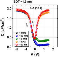
Fig. 57. Bidirectional C–V characteristics of GeO2/Ge stack with ∼1.5 nm EOT GeO2 grown on Ge(111) by LT-HPO (500 °C, 70 atm) for 5 min at frequencies from 100 Hz to 1 MHz. Nearly perfect C–V characteristics are obtained.
Download figure:
Standard image High-resolution image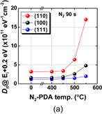
Download figure:
Standard image High-resolution image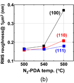
Fig. 58. (a) Surface orientation dependence of Dit values at Ei + 0.2 eV as a function of additional N2-PDA temperature. (b) Surface orientation dependence of rms roughness in a 1 × 1 µm2 area at the GeO2/Ge interface as a function of additional N2-PDA temperature. The GeO2/Ge(111) interface is the most robust against both Dit degradation and roughness increase in N2-PDA.105)
Download figure:
Standard image High-resolution image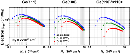
Fig. 59. Effective electron mobility in Ge n-MOSFETs fabricated on Ge(111), (100), and (110) substrates (NA = 2 × 1015 cm−3) with LT-HPO GeO2, as a parameter of additional N2-PDA temperature (L/W = 100 µm/90 µm). The (111) surface exhibits the highest electron mobility even after additional N2-PDA at 550 °C. This means Ge(111) is the most robust against further additional thermal process.105)
Download figure:
Standard image High-resolution image4.2. Low-oxygen-potential oxides
Considering both the conduction band offset at GeO2/Ge (∼1.6 eV54)) and the relative dielectric constant of GeO2 (∼6), the thinning limit of EOT of GeO2 will be estimated to be approximately 1–1.5 nm, by considering that in SiO2/Si MOS106) because a key parameter in the direct tunneling in the gate dielectric film is  (φ: band offset). Therefore, we will be able to reduce the GeO2 EOT on Ge down to ∼1 nm. However, considering that Ge should be beyond Si, high-k gate dielectric films are inevitably needed instead of GeO2, in addition to the LT-HPO method. We have fortunately found a good way of solving this matter as described in the following.
Now, we go back to thermodynamics. A remarkable job of HPO on Ge is based on the decrease in the Gibbs free energy change ΔG in the Ge oxidation process thermodynamically, as discussed in Sect. 2.1. There is another way of lowering ΔG in the oxidation. It is to replace HPO-GeO2 with another oxide having a lower ΔG° (the standard Gibbs free energy change per O2 molecule at 1 atm p-O2). That is, we can stabilize Ge gate stacks using low-oxygen-potential oxides instead of HPO-GeO2. We can search for candidate oxides in the Ellingham diagram.107) Figure 60 shows ΔG° as a function of temperature for various oxides. Consider the following reaction:

in which M is a metal. A lower ΔG° means in principle a more stable oxide (higher formation energy). It is clear that SiO2 is much more stable than GeO2. Interestingly, many rare-earth oxides and transition metal oxides are much more stable than SiO2. The reaction constant K in Eq. (4.1) is given by
Thus,

It is assumed in the above equation that O2 is only gas phase in the reaction. In the equilibrium state, ΔG = 0. ΔG° for a specific oxide can be obtained as the equilibrium oxygen vapor pressure.

Therefore,
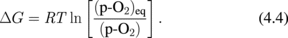
This relationship explains why HPO is very effective in stabilizing GeO2 in the simple Ge oxidation. More interestingly, it points to the fact that selecting a lower ΔG° oxide among various oxides (instead of or in addition to using HPO) is another way of achieving more stable gate stacks on Ge. ΔG is of course further decreased with an increase in p-O2. Thus, it naturally follows that HPO-Y2O3 is one of the most promising candidates on Ge. Note, however, that not all dielectric films with a lower ΔG° will be appropriate for gate stacks, as was the case of high-k material selection on Si.108) Y2O3 is fortunately what we have empirically regarded as the "Ge-friendly dielectric" for Ge gate stacks.61) Furthermore, we know that the interface is much better in Y2O3-doped GeO2 (YGO) than in pure Y2O3, as discussed in Sect. 3.2.64) Now, it is evident that YGO instead of GeO2 should be our target dielectric.109)

Fig. 60. Standard Gibbs free energy change associated with one oxygen molecule reaction, ΔG°, for the binary oxide formation of metals as a function of temperature (Ellingham diagram107)). It is obvious that GeO2 is rather unstable compared with other oxides.
Download figure:
Standard image High-resolution imageYGO films were deposited on Ge using the rf co-sputtering of GeO2 and Y2O3. It is worthwhile to show the GeO desorption temperature and water etching rate of 10%-Y2O3-doped GeO2 (YGO) and Sc-doped GeO2 (ScGO) together with those of pure GeO2 in Figs. 61(a) and 61(b).110) Doping only 10% Y2O3 (Sc2O3) into GeO2 significantly strengthens the GeO2 film. The interface layer formation through YGO in O2 PDA at 550 °C was estimated by CET increase in gate stacks with 10 and 30% YGO. Figure 62 actually shows no increase in capacitance equivalent thickness (CET) even in the 10% YGO case, while CET increase is significant in the case of pure GeO2. This indicates that YGO suppresses the O and/or VO diffusion kinetically as well as stabilizes the GeO2 film thermodynamically. Figure 63 shows the Y2O3 concentration dependences of the (a) relative dielectric constant and (b) water etching rate. k is above 8 even in 10% YGO, and almost saturates to be 10 in 20% YGO. No water etching is actually observed in 20% YGO.109)
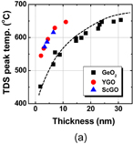
Download figure:
Standard image High-resolution image
Fig. 61. (a) GeO desorption peak temperatures of 10% YGO, 10% ScGO, and pure GeO2/Ge stacks in TDS measurements as a function of oxide thickness. Putting 10% Y2O3 or Sc2O3 into GeO2 increases the desorption temperature significantly. (b) Thickness reduction of doped and pure GeO2 by immersion into deionized water. The thickness was estimated by XPS. YGO and ScGO exhibit water robustness, although a small decrease of the thickness in YGO and ScGO might be due to the etching of Y(Sc)-insufficient GeO2 at the surface.110)
Download figure:
Standard image High-resolution image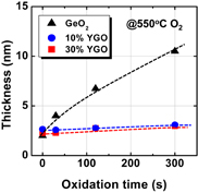
Fig. 62. Increase in oxide thickness in ∼2-nm-thick YGO (10 and 30% Y)/Ge and GeO2/Ge stacks as a function of additional oxidation time at 550 °C. Almost no additional oxidation is observed in the YGO/Ge stack, which means YGO is a strong barrier against the oxygen diffusion.109)
Download figure:
Standard image High-resolution image
Download figure:
Standard image High-resolution image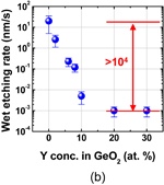
Fig. 63. (a) Relationship between Y concentration and the relative dielectric constant k of YGO. k is sharply enhanced below 20% Y in YGO, followed by a gradual increase to Y2O3.109) (b) rate of YGO etching by deionized water.
Download figure:
Standard image High-resolution imageDit on Ge is shown as a parameter of Y% together with HPO-grown pure GeO2 in Fig. 64(a), together with the remarkable C–V characteristics of 10% YGO MOS capacitors in Fig. 64(b). The 10% YGO case is actually the same as the HPO-grown pure GeO2 case. Dit is degraded above 20% in YGO. This might be due to the phase segregation with a miscibility boundary around 15% YGO between Y-doped GeO2 and Y-germanates.111) Such a low Dit certainly should enable the achievement of very high electron and hole mobility values, as high as those in HPO-grown GeO2 gate stack MOSFETs on H2-annealed Ge(111). As shown in Fig. 65, the highest electron mobility is obtained in the 10% YGO case.109) All of the results so far obtained strongly suggest that YGO has a great potential for scaled Ge gate stacks. Note that no HPO was used for YGO in this experiment.

Download figure:
Standard image High-resolution image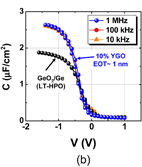
Fig. 64. (a) Energy distribution of Dit in various %Y-doped YGO/Ge stacks. Of the 6%-, 10%-, and 20%-doped YGO samples, the 10% YGO/Ge stack has the best interface. Dit similar to that in a GeO2/Ge stack formed by HPO+LOA was obtained. (b) Bidirectional C–V characteristics of 10% YGO/Ge and GeO2/Ge gate stacks with 2.3 nm physical thickness for both YGO and GeO2. The YGO/Ge stack was annealed at 500 °C for 30 s in N2. Considering that the EOT was only about 1 nm, the C–V characteristics are surprisingly good.111)
Download figure:
Standard image High-resolution image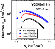
Fig. 65. Effective electron mobility in Ge n-MOSFETs with 6%-, 10%-, and 20%-doped YGO/Ge gate stacks. As expected from the results in Fig. 64(a), the highest electron mobility is shown in the 10% YGO case.109)
Download figure:
Standard image High-resolution imageWe investigated various M2O3-doped GeO2 including Al2O3 in terms of Dit. YGO was the best of those evaluated in our experiments, although the best property quantitatively may, of course, depend on the optimization level. Therefore we focus on YGO in the following section. Further material properties and structural consideration of YGO are discussed in Sect. 5 in conjunction with the gate stack reliability.
4.3. High-k material selection for further EOT scaling
Ge is more reactive to high-k materials than Si. This is an advantage in the sense that the interface GeO2 layer might be efficiently removed, as well as a disadvantage in the sense that the channel interface might be degraded by the mixing of Ge with high-k materials. The difficulty is that the advantage and the disadvantage have the same origin. However, we have to keep in mind that it was impossible to bring high-k technology into the CMOS platform before 2000. If we understand the high-k/Ge interface deeply, we should certainly be able to overcome this challenge.
As discussed in the previous section, YGO is one of the most promising candidates for Ge gate stacks. Since the dielectric constant of YGO is not so high, however, a real high-k layer on YGO is needed for further EOT reduction. Since the interface layer (IL) might readily intermix with the high-k material during the thermal process, high-k dielectrics should be designed in consistency with the YGO-IL. Figure 66 shows that a YGO-IL thicker than 1 nm can sufficiently suppress the cation diffusion from the top HfO2, while further downscaling results in a marked interface degradation.112) Therefore, HfO2 will not be a good choice for scaled gate stacks on Ge, even in cases with YGO-IL. We would like to propose YScO3 as a high-k dielectric film on YGO. Figure 67 shows that YScO3 is a real high-k material (k ∼ 17), although both Y2O3 and Sc2O3 have only medium-k values.113) Structural relaxation and denser packing in YScO3 might be the origin of the k-enhancement.114) In addition, YScO3 is also reported to have a sufficient energy band gap (∼6 eV).115) Note that a most beneficial point of YScO3 is that this material, unlike Hf on Ge, does not degrade the gate stack even if Y and/or Sc may diffuse to the interface, because both binary oxides are Ge-friendly and have the lowest ΔG°.
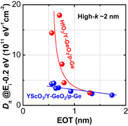
Fig. 66. Dit at Ei − 0.2 eV in YScO3/YGO/Ge(111) and HfO2/YGO/Ge(111) stacks as a function of EOT. The thicknesses of YScO3 and HfO2 were fixed at 2 nm, and the EOT was changed by the YGO interlayer thickness. With decreasing YGO thickness, the top HfO2 layer sharply degrades the Ge interface by a reaction through the interlayer, while YScO3 maintains the same interface quality down to the 0.5 nm region.112)
Download figure:
Standard image High-resolution image
Download figure:
Standard image High-resolution image
Fig. 67. (a) Photoabsorption spectra of Y2O3, Sc2O3, and YScO3 measured with the spectroscopic ellipsometer, and (b) relative dielectric constant k and optical band gap. Note that a high-k film is formed by combining two medium-k dielectrics.113)
Download figure:
Standard image High-resolution imageTo demonstrate aggressive EOT scaling into the deep sub-nm EOT regime, a thin YGO-IL was deposited, followed by the deposition of ternary YScO3 instead of a high-k binary oxide. Figure 68(a) shows well controlled C–V characteristics in YScO3/YGO/Ge gate stacks with EOTs as thin as 0.5 nm. The gate leakage current is shown in Fig. 68(b) as a function of EOT for various gate stacks. The YGO interlayer with YScO3 and HfO2 looks quite promising in terms of the gate leakage current, but when Dit is considered in Fig. 66, the YScO3/YGO gate stack is the most probable. YScO3/YGO/Ge(111) n-FETs were fabricated to verify the robustness of the present gate stack design.112) As shown in Fig. 69, the peak electron mobility of 1,057 cm2 V−1 s−1 was obtained with 0.8 nm EOT, thanks to a lower Dit than the HfO2/YGO case. Thus, it is safely concluded that YScO3/YGO/Ge is the most promising and realistic gate stack with a 0.5 nm EOT.112) (We used a 0.8 nm EOT gate stack for the mobility extraction, just because our FET was large and the gate leakage current made accurate mobility analysis difficult in 0.5 nm EOT region.)
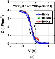
Download figure:
Standard image High-resolution image
Fig. 68. (a) Bidirectional C–V characteristics of aggressively scaled YScO3/YGO/p-Ge(111) stack with 0.5 nm EOT. (b) Gate leakage current, Jg, comparison of several gate stacks fabricated in our lab, (1) YScO3/YGO/p-Ge, (2) HfO2/YGO/p-Ge, (3) LTO-HPO-Y2O3, (4) 10% YGO/Ge, and (5) LTO-HPO-GeO2 with EOT thinner than ∼3 nm.112)
Download figure:
Standard image High-resolution image
Fig. 69. Effective electron mobilities of YScO3/YGO/Ge(111) and HfO2/YGO/Ge(111) n-MOSFETs in which YGO thickness is fixed at 1 nm. Note that the peak electron mobility with 0.8 nm EOT is 1057 cm2 V−1 s−1.112)
Download figure:
Standard image High-resolution imageHere let us summarize the electron effective mobility for both peak and high-Ns region as a function of EOT in gate stacks with GeO2/Ge, as shown in Figs. 70(a) and 70(b)109) and with YGO/Ge in Fig. 71.112) By taking care of materials (thermodynamics) and processes (kinetics), we can reduce EOT without degrading either peak or high-Ns electron mobility values. This is wonderful news for making Ge CMOS devices more viable.
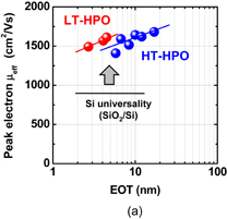
Download figure:
Standard image High-resolution image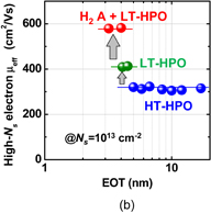
Fig. 70. Relationship between EOT and (a) peak electron mobility and (b) high-Ns electron mobility at Ns = 1 × 10¹³/cm2 in Ge(111) n-MOSFETs with GeO2/Ge gate stacks. No considerable degradation of the peak electron mobility is observed with decreasing EOT, and high-Ns electron mobility is enhanced by H2 annealing + LT-HPO.109)
Download figure:
Standard image High-resolution image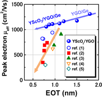
Fig. 71. Benchmark of the peak electron mobility in Ge n-MOSFETs as a function of EOT, by including recent reports in the literature. Note that the top high-k material is quite important for maintaining the high mobility in the sub-nm EOT region. The YScO3/YGO/Ge stack enables the high electron mobility to be maintained down to 0.8 nm EOT and is surely feasible at 0.5 nm EOT.112) [References: (1) C. H. Lee et al., IEDM 2013, p. 40, (2) S. Takagi et al., IEDM 2012, p. 505, (3) R. Zhang et al., IEDM 2011, p. 642, (4) W. B. Chen et al., IEDM 2010, p. 420, and (5) C. M. Lin et al., IEDM 2012, p. 509.]
Download figure:
Standard image High-resolution image5. Assuring Ge gate stack reliability
Ge gate stack properties have so far been intensively discussed in terms of the C–V characteristics and scalability by putting emphasis on thermodynamics and reaction kinetics. Next, we need to design reliability-aware gate stacks on Ge, particularly in the scaled EOT region. Concerning Ge gate stacks, Ge MOSFET performance has been improved considerably, but the reliability has been little investigated so far. Even the poly-Si/SiO2/Si system has a long history of reliability studies from intrinsic and extrinsic viewpoints,116,117) and reliability research is still seriously and carefully underway.118,119) It is the last and the most critical issue in device/process technology.
Reliability should be considered from various aspects and should also be statistically characterized for devices fabricated under well-controlled conditions. This kind of consideration, however, is generally not applicable for devices with new materials or new processes. Nevertheless, we should figure out the most critical aspect of the reliability. Otherwise, the feasibility of a gate stack cannot be estimated at all. Thus, in this review, we discuss only the essential parts of the reliability involved in Ge gate stacks, by characterizing the trap generation, Dit formation, and dielectric breakdown, because those are fundamentals in gate stack reliability. We pay particular attention to M2O3-doped GeO2 by comparing it with pure GeO2 from the viewpoint of network structure strength in dielectric films. To discuss the FET reliability, the device structure should generally be specified. Since that is beyond the scope of our reliability discussion in this paper, we discuss only simple planar gate stack reliability. Although we know much more data are definitely needed for the device reliability consideration, we would like to figure out only key factors using a small number of devices.
The most important conclusion we have recognized in Ge gate stack reliability is that good gate stack characteristics at the initial stage do not necessarily guarantee long-term device reliability.
5.1. Initial traps and trap generation
Several kinds of typical gate stacks on Ge were first compared from the viewpoints of initial trap density and trap generation. Each film was prepared by the same process for systematic study, and HPO-GeO2 was always included for comparison.
Figure 72(a) shows a schematic image of the trap filling process at a low electric field, and Fig. 72(b) shows VFB shift as a function of stress time for Y-, Sc-, and Al-doped GeO2 (YGO, ScGO, and AGO) and HPO-GeO2/Ge stacks at a low stress field (Estress = 4 MV/cm).120) Estress is defined by VOX/EOT, not only because it is a fair comparison concerning the practical device application but also because it is compatible with the thermochemical model for the dielectric degradation of high-k films.117) Very small VFB shifts suggest that the initial gate stack properties are very good for any of the dielectric films on Ge investigated in the present experiments. Next, the difference in trap generation among YGO, ScGO, AGO, and HPO-GeO2 under high positive field stress is shown in Fig. 73.120) Although we experimentally do not have the thickness dependence of VFB shifts, we can compare those films by assuming that the traps are generated close to the interface. Note that YGO shows the lowest trap generation rate under the present stress condition. On the other hand, the HPO-GeO2/Ge gate stack is significantly degraded under high field stress, though it shows good initial C–V characteristics. Because the SiO2/Si system is always the reliability reference and the best as compared with newly developed ones, it is surprising that the GeO2/Ge system is much worse than the YGO/Ge one. This is one of the most important findings in Ge gate stack reliability, and it is worthwhile considering why YGO is better than GeO2 on Ge. Next, let us discuss about it from the viewpoint of the network structure strength in dielectric films.
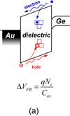
Download figure:
Standard image High-resolution image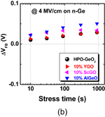
Fig. 72. (a) Schematic of trap filling process for electrons and holes in gate dielectric film under a low electric field (low Estress), in which Estress is defined by Vg/EOT. (b) Flat-band voltage shift (ΔVFB) for HPO-GeO2, AGO, ScGO, and YGO/Ge stacks under Estress = 4 MV/cm, as a function of stress time. By simply assuming ΔVFB = qNt/Cox, Nt ∼ 3 × 1011 cm−2 is estimated (Nt: trap density and q: electron charge).120)
Download figure:
Standard image High-resolution image
Fig. 73. Generated electron trap density calculated from ΔVFB in HPO-GeO2, AGO, ScGO, and YGO/n-Ge stacks under positive Estress = 9 MV/cm for 90 s. The trap generation is the most suppressed in YGO gate stacks.120)
Download figure:
Standard image High-resolution image5.2. Network flexibility and rigidity
Why does YGO or ScGO have a lower trapping generation rate than GeO2? It will be reasonable to consider that electrical reliability is directly connected to structural stability in gate dielectric films, because gate stack degradations such as the trap generation and dielectric breakdown should be triggered by the local bond breaking in the network structure of the dielectric films. Since the water etching rate of YGO is much less than that of GeO2 as shown in Fig. 63, the YGO network should be much stronger than the GeO2 one. A local bond rearrangement in network structure rather than a single bond breaking may be more critical in the high field stress. Namely, the lower level of trap generation rate in YGO on Ge is considered to be due to the fact that Y cations in GeO2 may strengthen the structural network of GeO2.120) Therefore, the impact of structural change on the dielectric properties is next discussed systematically.
We introduce a "rigidity" in order to quantitatively characterize a topological concept of the structural network in dielectric films.121) Let us define the rigidity of dielectric films by both single bond strength and network strength as follows:

where γ is a prefactor (dimensionless) representing the single bond strength. The value of γ is assumed to be 1 for SiO2. Oxides with a metal–oxygen (M–O) single bond stronger or weaker than that of Si–O have a γ value larger or smaller than 1, respectively. Note that γ < 1 for both GeO2 and conventional high-k materials. Suppose that Nav is an average of the coordination number of each atom in the network, as already defined by Lucovsky et al.:122)
Figure 74(a) shows the Nav of YGO calculated by assuming its possible network structures, as a function of Y-ratio in YGO. Nav(YGO) was calculated by assuming that the coordination number of Y was 7, as follows:

Here, x = Y/(Y + Ge). Figure 74(b) shows a schematic image of the effect of Y addition on GeO2 network. YGO is regarded as the modified random network structure. Here, γ is assumed to be 0.8 in GeO2, because the bond strength of Ge–O is 0.8× that of Si–O, although γ might be lower than 0.8 in Y-rich YGO,121) which is shown in Fig. 74(a). By defining the rigidity, we can compare the network robustness among different dielectric films. Namely, we think that the trap generation is not a simple bond breaking but a local network rearrangement around the broken bond. Thus, the rigidity is more important than the single bonding energy. As a result, GeO2 (rigidity ≃ 2.1) is more flexible than the moderately rigid SiO2 (rigidity ≃ 2.67), but it is less robust against an external stress than SiO2 because of its smaller rigidity.
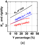
Download figure:
Standard image High-resolution image
Fig. 74. (a) Average coordination number (Nav) and rigidity of YGO as a function of Y doping concentration. γ is actually not a constant but reduced with Y% increase in YGO (red line). (b) Schematic structural image of Nav increase with Y% increase in the network structure of YGO.121)
Download figure:
Standard image High-resolution imageThe concept of the rigidity is not new in the continuous random network (CRN) type of amorphous films and has already been discussed topologically in the glass community.123,124) We have applied this concept to sub-nm EOT dielectric films on Ge in terms of the cation introduction into GeO2. This is the first case that the rigidity is redefined by taking account of the single bond strength in addition to Nav. The Nav concept was also conjectured in gate stacks on Si by nitrogen (cation) doping into SiO2,125) but as discussed here, the cation doping changes GeO2 more considerably and favorably.
Figure 75 suggests schematically that a lower rigidity (with a low Nav and the same γ) leads to a lower  and
and  at the initial stage. We assume that
  shows a parabolic dependence on the rigidity as follows:

where  is the reference rigidity of a very flexible network. The parabolic dependence of the initial
  on the rigidity seems intrinsic at the interface because a mechanical strain on each atom might be involved in the initial
  . A similar parabolic type of dependence has been reported in the anion-doped case in SiO2/Si gate stacks.125) Consequently, a lower rigidity will be more appropriate for better initial properties. In contrast, in a very rigid network, higher coordination puts more constraints on the ions, exceeding their degree of freedom. Higher rigidity in dielectric films therefore initially results in a higher probability of bond breaking and trap formation. On the basis of above topological concept of dielectric film network structure, we can understand experimental results of the initial interface states density (
 ) and preexisting trap density (
 ) in dielectric films with different rigidity values on Ge.
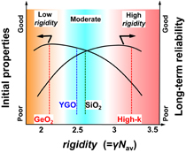
Fig. 75. Phenomenological trade-off view of initial film properties with dielectric film reliability as a function of rigidity. In the low-rigidity region, the interface might be good, thanks to a flexible network both in the bulk and at the interface, but reliability should be poor due to rather easy bond breaking. On the other hand, it is opposite in the high rigidity case. Thus, a moderate rigidity system (SiO2/Si or YGO/Ge) is practically favored for maintaining both good interface and long-term reliability. Here, γGeO2 = 0.8 and γSiO2 = 1 are assumed from the bonding energy consideration.121)
Download figure:
Standard image High-resolution imageNext, we conjecture the gate stack reliability against high electrical stress. We think that the gate stack degradation should originate from the network deformation in the bulk or at the interface triggered by a local bond breaking. Therefore we intuitively define the energy to deform the dielectric film network as follows:

where Δdeform is the energy needed to deform the network and Δ0 is an energy constant. To verify the relationship between rigidity and reliability, the degradation of gate stack properties was directly compared between flexible HPO-GeO2/Ge and moderately rigid YGO/Ge. The experimental data plotted in Fig. 76(a) show that under a high positive Estress, the YGO/Ge gate stack shows a lower Dit generation rate than the more flexible GeO2/Ge. Since HPO-GeO2 was easily broken down in case of high negative Estress, only the positive Estress results are shown. This is direct evidence that GeO2/Ge layer is much weaker than YGO/Ge, although the degradation mechanism should be further studied. The same trend was found in the bulk trap (Nt) generation, which was estimated from the stress-induced leakage current (SILC) under Estress = +9 MV/cm, as clearly shown in Figs. 76(b) and 76(c). As shown schematically in Fig. 77, the energy needed to break all the bonds and displace the ions in a rigid network is likely to be higher than that needed in a flexible one.120)
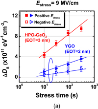
Download figure:
Standard image High-resolution image
Fig. 76. (a) Dit increase at Ei − 0.2 eV in HPO-GeO2/ (EOT = 3 nm)/ and YGO (EOT = 2 nm)/Ge(111) stacks under both positive and negative Estress = 9 MV/cm as a function of stress time. Under negative Estress, HPO-GeO2/Ge was easily broken. (b, c) Gate leakage current density increases in HPO-GeO2 and YGO/Ge gate stacks after positive Estress = +9 MV/cm for 0, 10, 30, 90, and 300 s. In the YGO/Ge case, a much less leakage current increase is observed.120)
Download figure:
Standard image High-resolution image
Fig. 77. Schematic images suggesting both the modification of GeO2 network and the robustness against trap generation under high Estress by Y doping, attributable to the rigidity increase with Y introduction into GeO2.120)
Download figure:
Standard image High-resolution imageBy comparing our model with the thermochemical model,117) the trap generation rate g can be described as follows:
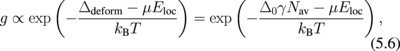
where μ is the local dipole moment and Eloc is the local electric field. Both sets of experimental results are consistent with our view that the higher rigidity in YGO can make GeO2 more robust against high electrical stress. Namely, good initial passivation should be compromised with the long-term reliability, in addition to the process robustness and EOT scalability. Thus, it is emphasized that an IL with a moderate rigidity such as YGO is better to integrate with high-k dielectrics than GeO2-IL, even if a decent C–V curve is initially obtained in high-k/GeO2/Ge gate stacks.
The rigidity model is not quantitative but rather intuitive. Nevertheless, we think that the rigidity is a useful concept for achieving both good initial and highly reliable properties in MOS gate stacks including other semiconductors, although much more data are needed.
5.3. Reliable scaled Ge gate stacks
To further demonstrate substantial effects of the rigidity control on the gate stack reliability, we prepared a moderately rigid dielectric 10% YGO/Ge followed by PDA in LT-HPO at 500 °C, which enabled the YGO film to be made further Vo-free. Moreover, EOT extracted from C–V characteristics was very slightly changed in LT-HPO PDA, which means that further Ge oxidation was negligible in this additional PDA.121) Figure 78(a) shows a very low Dit at the LT-HPO-YGO/Ge interface thanks to the sufficient flexibility of the HPO-YGO network and well-controlled process condition. The VFB shift is also negligible under Estress = 4 MV/cm with both polarities as shown in Fig. 78(b), which shows that  values are lower than 9 × 1010 cm−2 for both electron and hole traps in as-prepared LT-HPO-YGO/Ge gate stacks. Related to the low
  , the initial gate leakage current in LT-HPO-YGO/Ge is comparable to that in the YGO/Ge stacks. SILC is also surprisingly small in LT-HPO-YGO/Ge gate stacks, as shown in Figs. 79(a) and 79(b) for both the positive and negative polarity stress cases. Figures 80(a) and 80(b) show JG increase and Dit generation under the positive 9 MV/cm stress, respectively, for HPO-GeO2, YGO, and LT-HPO-YGO gate stacks. The GeO2/Ge stack is easily degraded though its initial characteristics appear rather better. Note also that LT-HPO-YGO may have the same trap generation origin as YGO, because the slope in Fig. 80(a) is almost the same in the form of ∼αtn, while it is much better than YGO in terms of Dit generation. The stress field polarity dependence of Ge gate stack reliability is apparently the same as that of SiO2/Si gate stacks, but it seems to be more significant. Although the poorer GeO2/Ge interface is likely to be the origin, further study is needed.
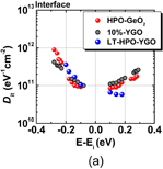
Download figure:
Standard image High-resolution image
Fig. 78. (a) Dit spectra in HPO-GeO2, 10% YGO and LT-HPO-YGO stacks measured by the low-temperature conductance method. (b) VFB shift in LT-HPO-YGO/Ge stack as a function of stress time under Estress = 4 MV/cm. All films show very good interfaces and low initial trap densities.121)
Download figure:
Standard image High-resolution image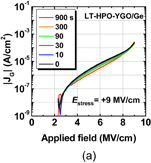
Download figure:
Standard image High-resolution image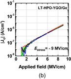
Fig. 79. Leakage current change in LT-HPO-YGO/Ge stacks (EOT = 2 nm) stressed under (a) Estress = +9 MV/cm and (b) Estress = −9 MV/cm, as a function of stress time for 0, 10, 30, 90, 300, and 900 s. No increase in JG is actually observed even after high Estress for both polarities.121)
Download figure:
Standard image High-resolution image
Download figure:
Standard image High-resolution image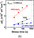
Fig. 80. (a) Leakage current measured at 6 MV/cm in HPO-GeO2, YGO, and LT-HPO-YGO/Ge stacks as a function of stress time under Estress = +9 MV/cm. (b) Increase in Dit at Ei − 0.2 eV in HPO-GeO2, YGO, and LT-HPO-YGO/Ge stacks by Estress = +9 MV/cm as a function of stress time. In both cases, LT-HPO-YGO and HPO-GeO2 show the best and the worst, even though their initial characteristics are not so different from each other.121)
Download figure:
Standard image High-resolution imageFurthermore, the effect of top high-k materials (YScO3 and HfO2) on gate stack reliability is discussed for the YGO-IL case for further EOT scaling. As shown in Fig. 81, YScO3/YGO/Ge shows a much smaller VFB shift than HfO2/YGO/Ge under two kinds of high negative Estress conditions. Although both have EOT = 0.8 nm, the VFB shift as a function of the stress time differs significantly between them. This implies that top high-k films should be selected by taking account of their reliability, particularly for the sub-nm EOT region. YScO3, unlike Hf on Ge, does not degrade the gate stack even if Y and/or Sc may diffuse to the interface, as already discussed in Fig. 66. Figure 82 demonstrates that, thanks to the suppression of trap generation, YScO3/YGO/Ge can survive a much longer time than HfO2/YGO/Ge under considerably high voltage conditions, although more data are obviously needed to discuss the breakdown lifetime. All the experimental results obtained so far indicate that the rigidity concept is quite useful for the reliability consideration of Ge gate stacks.
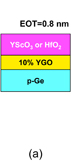
Download figure:
Standard image High-resolution image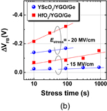
Fig. 81. (a) Schematic of the test sample structure. (b) VFB shift for YScO3/YGO and HfO2/YGO/Ge stacks with 0.8 nm EOT as a function of negative stress time. The upper high-k film significantly affects gate stack reliability in the sub-nm EOT region.
Download figure:
Standard image High-resolution image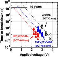
Fig. 82. Preliminary results of the time to breakdown for HfO2/YGO (EOT = 0.8 nm), YScO3/YGO (EOT = 0.8 nm), and YGO/Ge (EOT = 2 nm) stacks as a function of applied voltage. The maximum oxide voltage projection in 10 years is roughly estimated. YScO3/YGO gate stacks show promising reliability for ∼0.7 V operation, although much more tests should be carried out for the reliability projection statistically.
Download figure:
Standard image High-resolution imageA wrong view that GeO2/Ge should be the best for Ge gate stack has often been addressed. We also considered that it would be. In this paper, we have proposed the new concept of the rigidity of dielectric films for achieving both reliable and scalable Ge gate stacks; resultantly, we have found that the GeO2/Ge gate stack has an intrinsic weakness against electrical stress. We do not hesitate to say that a dielectric film with moderate rigidity should be employed to satisfy good initial passivation, process robustness, and long-term reliability simultaneously in scaled Ge gate stacks.121) Nevertheless, there is no question about the fact that a detailed understanding of GeO2/Ge should be the basis of Ge gate stack design.
The reliability study of Ge gate stacks started just a couple of years ago.56,126–128) Most of reliability studies have focused on the BTI stress in Ge or Ge-rich SiGe p-MOSFETs, since p-MOSFETs are now in more urgent need. The interface defect generation models proposed so far have tried to explain experimental results by considering the defect distribution in space and energy. This is the same method as carried out in Si CMOS reliability assessment. Most of the proposals are based on the conventional band-diagram perspectives, and few studies from materials viewpoints have been reported. We have discussed Ge gate stack reliability from a more material engineering viewpoint in conjunction with well-controlled gate stack formation. We would now hesitate to quantitatively assess the reliability of Ge gate stacks. Nevertheless, we surely have to recognize that GeO2/Ge is unlikely to meet the reliability requirements. This has also been recently reported by another group.126) The gate stack reliability has usually been discussed as a function of stress time, and then the degradation kinetics in gate stacks has been conjectured. However, the same strategy is not always applicable for new materials. We believe that a key guideline such as the rigidity is needed for establishing the reliability framework in Ge devices.
6. Reducing contact resistance and junction leakage
The contact resistance is an intrinsic hurdle against enhancing the FET performance. This is of course true for Si devices as well. In fact, the contact resistivity ρc is expressed as
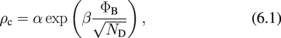
where α, β, ΦB, and ND are, respectively, two constants, Schottky barrier height (SBH), and active dopant concentration. Since the actual contact resistance is inversely proportional to the square of scaling factor, it is serious in device miniaturization.129) Furthermore, it is even severer in Ge FETs for two reasons. One is the almost perfect Fermi-level pinning (FLP) at the metal/Ge interface, which makes the metal selection meaningless, and the other is the relatively low impurity solubility in Ge. Therefore, understanding and controlling the FLP and dopant activation are crucially important for achieving high-performance Ge n-MOSFETs.
The FLP is directly related to the SBH formation mechanism. According to introductory solid-state physics textbooks, the SBH is in principle determined by the difference between the metal work function ΦM and the semiconductor electron affinity χ, as shown in Fig. 83. However, it is very rare that SBH is described as above. Generally, SBH obtained experimentally is between ideal and perfect pinning. Using the pinning parameter S, the SBH ΦB is expressed as130)

where ΦM, ΦCNL, and χ are respectively the metal work function, charge neutrality level, and electron affinity. All values above are defined from the vacuum level. The charge neutrality level ΦCNL of surface states is the position at which the surface net charge is zero, whatever the FLP mechanism is. In case that EF is above the ΦCNL, the surface is negatively charged, while in case that EF is below the ΦCNL, the surface is positively charged.130) S = 1 corresponds to the Schottky limit with no pinning, while S = 0 corresponds to the Bardeen limit with the perfect pinning, in which the metal work function has nothing to do with the Schottky barrier height. There are so many publications on the mechanism of SBH formation.131–135) Since this research field includes a number of basic models as well as practical engineering, we do not like to generally discuss the FLP but would like to share something about the fantastic characteristics of FLP on Ge.

Fig. 83. Band alignment at metal/semiconductor interface based on the ideal Schottky–Mott model. ΦB is Schottky barrier height, and ΦM and χ are the work functions of a metal and electron affinity of a semiconductor, respectively.
Download figure:
Standard image High-resolution imageThe higher doping at the interface can in principle reduce the tunneling distance. However, there is the solubility limit of dopant in semiconductors. In case of phosphorus in Ge, about ∼2 × 1019 cm−3 is the maximum concentration in the equilibrium state reported experimentally. Several doping techniques have been reported in the literature to enhance the impurity concentration in Ge. Concerning the p/n junction leakage, we experimentally address an importance of the field isolation material surrounding the contact area in Sect. 6.2.
6.1. Schottky barrier height control
In metal/Ge junctions, the Fermi level of Ge is strongly pinned at the charge neutrality level (CNL) close to the valence band edge of Ge,136,137) which means S ∼ 0 in Eq. (6.2). It is said that gap states above and below the CNL serve as acceptor- and donor-type states, respectively. The CNL is in principle determined in the semiconductor side. A more detailed explanation considering the density of states in the conduction and valence bands is found in textbooks.130) To systematically investigate FLP, we prepared metal/Ge junctions using various metals with a wide range of vacuum work functions in UHV. All metal/p-Ge showed ohmic and all metal/n-Ge junctions showed Schottky diode characteristics. The effective work function, which was calculated from the experimental SBH by assuming the simple definition of the work function in Fig. 83, is plotted by comparing with the work functions of pure metals reported138) in Fig. 84.137) The CNL at the metal/Ge interface is estimated by plotting the SBH as a function of the pure metal work function in Fig. 85,137) and is close to the branch point calculated for the bulk Ge.139) Note that, in this experiment, not only the work function but also the interface conditions such as inter-reaction, inter-diffusion and/or morphology should differ from metal to metal on Ge. This suggests that the Fermi level of a metal at a metal/Ge interface is intrinsically pinned at the CNL of Ge, although the FLP mechanism is still under debate and no consensus has been reached yet.130) It is also regarded as the fact that the Fermi level in Ge is fixed at the CNL. Thus, we infer that the FLP on Ge is caused by the so-called metal-induced gap states (MIGS) mechanism because it is the only intrinsic mechanism so far proposed for the FLP at metal/semiconductor interfaces. In addition, the MIGS is theoretically more appropriate for narrower energy band gap semiconductors such as Ge, although the MIGS model cannot generally characterize the FLP on any semiconductors. It would be significantly useful in Ge device technology that we could manage to control the intrinsic FLP on Ge.
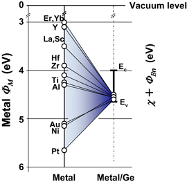
Fig. 84. Relationship between the vacuum work function of metal and experimentally estimated Schottky barrier height (actually,  ) on n-Ge are plotted. Despite various work function metals on n-Ge, almost no change in ΦBn is observed in Ge. This is called the Fermi-level pinning.137)
Download figure:
Standard image High-resolution image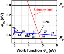
Fig. 85. ΦBn values on n-Ge for various metals. The slope of ΦBn against metal work function is defined as the pinning parameter S. In the Ge case, S ∼ 0.02. The charge-neutrality level (CNL) is estimated from the cross point with the Schottky limit line to be 0.08 eV from the valence band edge with the assumption of χGe = 4.0 eV.137)
Download figure:
Standard image High-resolution image6.1.1. Fermi-level pinning modulation: tunnel contact.
Owing to the strong FLP on Ge, ohmic characteristics for p-Ge and Schottky ones for n-Ge were experimentally observed regardless of the metal work function. On the other hand, as already discussed in previous sections, the flat-band voltage (VFB) and surface potential in Ge MIS capacitors are substantially modulated without showing the strong FLP at the metal/insulator and insulator/Ge interfaces, respectively. This suggests that the strong FLP observed at metal/Ge junctions should be substantially unpinned by inserting an oxide layer between metal and Ge. In addition, putting an insulator between the metal and Ge may alleviate the FLP because it may suppress the metal wave function evanescent into Ge. Thick oxide insertion, however, obviously cannot be used at source/drain junctions. Thus, we investigated the effect of inserting an ultrathin oxide (UTO) into the metal/Ge interface to alleviate the FLP.
Both n- and p-type Ge(100) substrates were used. GeO2 was used as the UTO on Ge. We first checked Ge MIS capacitor characteristics with thick GeO2 (15 nm). Both Au and Al electrodes were deposited on the same Ge substrate. In C–V characteristics at 1 MHz, the surface potential at the thick-oxide/Ge interface was of course controlled by gate bias, and a reasonable VFB difference at 1 MHz (0.8 V) was obtained between Al and Au gate GeO2/Ge MOS capacitors. Metal/Ge junctions on n- and p-Ge show Schottky and ohmic characteristics in Fig. 86(a), while very interestingly, the diode characteristics are totally changed by inserting thin GeO2 film as shown in Fig. 86(b). The reversely biased current density increases on n-Ge and decreases on p-Ge by increasing the interfacial GeO2 thickness, as shown in Figs. 87(a) and 87(b).140) This transition obviously indicates that the Fermi level of metal is effectively shifted toward the conduction band edge (CBE) of Ge by the UTO insertion, as expected above. Figure 88 shows the GeO2 thickness dependence of SBH alleviation. With an increase in the GeO2 thickness, the FLP on Ge is gradually alleviated, and it is seen that SBH goes back toward the value expected by the vacuum work function. Although the SBH estimated in metal/UTO/Ge junctions may include a potential drop across the UTO, the effective SBH enhancement observed on p-Ge cannot be simply explained by the potential drop. Furthermore, if the UTO film may act as the defect passivation at the interface, the SBH should shift more abruptly and then saturate with increasing GeO2 thickness. Thus, the results seem to support the MIGS model that the wave function tailing from the metal into Ge is essentially involved in the FLP.

Fig. 86. J–V characteristics of Al/Ge diodes and schematics of both sample and band alignment structures. (a) Although the work function of Al is relatively close to the electron affinity of Ge, Schottky diode and ohmic characteristics are observed on n- and p-Ge, respectively, owing to the strong FLP on Ge. (b) By inserting ultrathin GeO2 between Al and n-Ge, J–V characteristics are completely reversed.
Download figure:
Standard image High-resolution image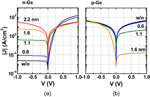
Fig. 87. J–V characteristics of Al/GeO2/Ge diodes. The off-state current increases (a) on n-Ge and decreases (b) on p-Ge with an increase in GeO2 thickness. In the ∼2-nm-thick GeO2 case, ohmic and Schottky diode characteristics are observed on n- and p-Ge, respectively.140)
Download figure:
Standard image High-resolution image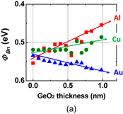
Download figure:
Standard image High-resolution image
Fig. 88. (a) Schottky barrier height ΦBn at Al/, Cu/, and Au/GeO2/Ge junctions as a function of GeO2 thickness. ΦBn changes with GeO2 thickness toward the value as expected from the vacuum work function of each metal. (b) The sample structure for the systematic measurement in this experiment is also shown.
Download figure:
Standard image High-resolution imageAlthough we considered that the UTO insertion technique was the first proposal and demonstration for tuning the SBH when we presented experimental results at IEDM 2007,60) we later found that this FLP alleviation method had been proposed by Connelly et al. for the FLP on Si.141) They reported that the SBH was modulated by 0.25 eV when an ultrathin Si3N4 film was inserted between Mg and Si from the MIGS suppression viewpoint. Now, the UTO insertion contact is called the tunnel contact using several insulators on Ge.142–148) Since TiO2, in particular, has a small band offset energy against the Ge (Si) conduction band edge, the tunnel resistance should be very small in terms of the tunnel contact.147)
However, since the pinning parameter is still very small (∼0.2) after the UTO insertion, the Fermi level seems to still be strongly pinned. In addition, this fact does not necessarily prove that the MIGS model is logically correct, and it is debated that the UTO thicknesses reported in the literature might be rather thick in terms of the suppression of wave function tailing. It should be further studied. Nevertheless, this method is the first experimental demonstration from the engineering viewpoint that metal can make an ohmic contact on n-Ge without any doping.
6.1.2. Fermi-level pinning modulation: electron density tuning in metals.
After our demonstration of the UTO insertion effect on FLP alleviation on Ge, several methods for modifying the FLP without inserting an insulator have been reported. amorphous (a-) TiN deposited by sputtering was demonstrated to make an ohmic contact to n-Ge.149) Figure 89 shows J–V characteristics both on n- and p-type Ge with TiN deposited by rf-sputtering. Increasing the rf-power seems to shift the pinning position from the valence band edge to the conduction band side. The apparent CNL shift seems to be the same as in the nitride insertion cases.142) The authors have considered an amorphous interlayer as a key to the FLP modulation, but the detailed physics underlying this shift is still under investigation.150)
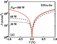
Download figure:
Standard image High-resolution image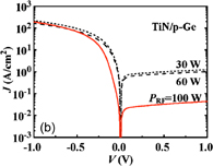
Fig. 89. J–V characteristics of TiN/amorphous TiGeN/Ge junctions fabricated by the sputtering of TiN on Ge, which reports that the Schottky–ohmic conversion is also observed by forming amorphous TiGeN between TiN and Ge.149) Reprinted with permission from Ref. 149. © 2011 AIP Publishing.
Download figure:
Standard image High-resolution imageIt has been reported that SBHs of metals such as Fe3Si,151) Mn5Ge3,152) Sn,153) and graphene154) on Ge deviate from the strong FLP trend. Recently, W-encapsulating Si cluster film insertion has also been reported.155) Most of those reports except graphene case maintain that the FLP on Ge is not determined by MIGS because SBH is modulated by changing the metal even in the direct metal/Ge structure. In case of graphene, they proposed the MIGS model because SBH changed with an increase in the number of graphene layers. Several UTO or ultrathin nitride (UTN) insertion methods reported in the literature actually seem to be in principle the same as ours, but the direct metal deposition cases are different in terms of both no potential barrier against the wave function tailing and the atomic ordering at the Ge interface in epitaxial metal cases. It is, however, difficult to conjecture the pinning mechanism because the work function has not been systematically characterized in those systems. As a result, the mechanism of FLP at metal/Ge interfaces is still controversial, although it is very favorable practically that various materials can be used as the ohmic metal on n-Ge.
Since SBH is in principle determined by both the metal work function and electron affinity of a semiconductor as shown in Fig. 83, the work function in metal is one of key elements in SBH. Therefore, let us consider what determines the work function in metals. It consists of both the bulk and surface parts, which is schematically described in Fig. 90(a). The bulk part Φb comes from many electron effects, while the surface part Φs is from the wave function evanescent to the vacuum, which forms the surface dipole.156) Although this view based on the jellium model is too simple for quantitative discussion, the work function trend in many simple metals can be described by this approach as shown in Fig. 90(b). With an increase in electron density in metals, the work function increases mainly due to the surface contribution increase. Since the surface part is in principle determined from the tunneling from the metal to vacuum, its penetration extent depends on the electron density and surface orientation of metals.157) We note that the surface part in the work function looks similar to the physical implication of MIGS originally proposed by Heine.158) A difference with respect to solid–vacuum interfaces is that the wave function tails oscillate at solid–solid interfaces due to the Bloch wave function nature in semiconductors, as schematically shown in Fig. 91. In more detail, the non-jellium contribution should of course be taken into account, but the electron density effect is expected to be qualitatively correct.156,159)
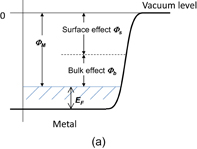
Download figure:
Standard image High-resolution image
Fig. 90. (a) Schematic description of work function of metal in vacuum. The vacuum work function consists of both bulk Φb and surface Φs terms. (b) Calculated bulk and surface terms of the vacuum work function as a function of free electron density in metal (replotted from Ref. 156). Note that Φs becomes dominant with free electron density increase.
Download figure:
Standard image High-resolution image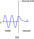
Download figure:
Standard image High-resolution image
Fig. 91. Schematics showing a similarity between (a) the surface term of vacuum metal work function at vacuum/metal interface and (b) the origin of MIGS model, from the viewpoint of wave function evanescent forming the interface dipole.
Download figure:
Standard image High-resolution imageWe have very recently studied the effects of metal on FLP from the aforementioned aspect. Technically speaking, if we believe that the FLP on Ge is mainly characterized by the MIGS model, we might control it by changing the electron density and surface orientation of the metal side, as expected from the work function theory. We prepared several kinds of germanides on n-Ge and measured their SBHs at room temperature. Although we do not presently know the exact work functions of germanides, the germanide with a rather low work function metal, GdGex shows the higher Ioff current on n-Ge(100), as shown in Fig. 92(a). This implies the smaller SBH at the GdGex interface. More interestingly, GdGex on n-Ge(111) exhibits ohmic I–V characteristics as shown in Fig. 92(b),160) although a direct Gd/Ge junction does not show appreciable surface orientation dependence. Figure 92(c) shows the cross-sectional TEM image of GdGex/Ge(111), in which no interfacial layer is observed. In the preliminary XRD analysis, Gd2Ge3 is likely,161) but a more detailed analysis is needed. The electron density in GdGex estimated by the Hall effect measurement was ∼7 × 1021 cm−3, which is ∼1 order of magnitude smaller than the electron density in conventional metals. Although the present result is not necessarily conclusive for the SBH formation mechanism on Ge, it is strongly suggested that the free electron density in metals has a significant effect on the SBH formation on Ge. The experiments are still preliminary but the results are exciting.

Download figure:
Standard image High-resolution image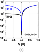
Download figure:
Standard image High-resolution image
Fig. 92. (a) Typical J–V characteristics of germanide and element metal/n-Ge(100) junctions. (b) Effect of Ge surface orientation on J–V characteristics of GdGex/n-Ge. Note that GdGex/n-Ge(111) shows ohmic characteristics. (c) Cross-sectional TEM image of GdGex/Ge(111) interface. The crystallized GdGex forms the direct interface on Ge substrate and no interfacial layer is observed. It is noted, however, that the GdGex layer is not epitaxially grown on Ge(111).160)
Download figure:
Standard image High-resolution imageMost of metal/Ge junctions reported so far149–155) seem to be consistent with this view. We do not maintain that the FLP mechanism at any metal/semiconductor junctions should be understandable from the MIGS model. And, we do not think a single mechanism always determines the FLP for a given semiconductor, including Ge, but a couple of mechanisms might work together. We think that the MIGS dominant behavior comes from the fact that Ge is a special semiconductor with a narrow energy band gap and a branch point near the valence band edge. Resultantly, both methods in the UTO insertion and in the electron density tuning can suppress the wave function tailing into Ge. The latter effect seems to be applicable for Si as well, in the recent experiment using Bi electrode.162)
Finally in this section, we would like to reconsider the work function ΦM used in Eq. (6.2), in which ΦM is the metal work function with the vacuum interface. As discussed in this section, the work function in itself consists of two components. One is the bulk component and the other is the surface one. This fact means that the work function is sensitive to the surface counterpart. Namely, the work function is not a material constant but should depend on what the counter material is. Now, we come to the question "Is the work function at the Schottky interface the vacuum one, ΦM ?" In fact, ΦM is very sensitive to the surface orientation and contamination. Therefore, we rewrite the metal work function on semiconductors as follows, by assuming that any finite shift from the Schottky limit may come from the work function modulation on semiconductors.

where  and
and  are the work functions in vacuum and on semiconductor, respectively. That is,

This equation means that  is determined by both ΦM and ΦCNL with the weight of S and 1 − S. In case of S = 1,
  , while generally
  should be affected by the intrinsic wave function evanescent from metal to semiconductor, which is considered as the MIGS origin, resulting in the interface dipole formation at metal/semiconductor interface. This is the intrinsic effect affecting the work function on semiconductors (insulators as well) in the pure limit. The interface has been generally considered as (
 ), but note that
  loses the physical meaning in a metal contacting with semiconductors. Thus, we would suggest that instead of such conventional view, the MIGS-type FLP can be regarded as the metal work function modulation (
 instead of
  ) in the Schottky limit, although the MIGS view is important in terms of the fact that
  is affected by the CNL in the semiconductor.
This view does not necessarily exclude extrinsic effects such as defects on the FLP. Equation (6.4) can be rewritten as

Suppose that there is another pinning origin at the interface, SD and  , and that the pinning is described by Eq. (6.2) with
  .
.
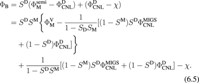
Therefore, by denoting S and ΦCNL as
Equation (6.2) is obtained again. Note that two pinning mechanisms are involved in this formula, although an interaction between two origins is not taken into account. In case that SM ∼ 0 ≪ SD < 1 (probably Ge case),

Thus, it is expected that ΦB has nothing to do with  , and that ΦCNL is affected by the extrinsic interface effect. Since Eq. (6.2) in itself is the phenomenological formula, more detailed analysis will not be meaningful. However, when the metal side effect on the FLP is considered as discussed above, the relationship between SBH and metal work function will become physically clearer, although the view that MIGS effect is equivalent with the work function modulation of metal at the Schottky interface should be further investigated theoretically. We think that this view might be true in case of semiconductors with relatively narrower energy band gap. This consideration discussed here may seem to be strange, because the MIGS theory is now widely accepted in this community. However, the work function modulation model may also be feasible, if it cannot be true that the work function of a metal in contact with semiconductor is as the same as that in vacuum. For more detailed discussion, the interaction of the metal with valence band electrons should be taken into consideration, which substantially determines the CNL in the semiconductor side, while it is no need in the vacuum case, although more rigorous theory is obviously needed for fully understanding metal/semiconductor interfaces.
6.2. n+/p junction
The lower doping solubility is a big concern in Ge CMOS technology in addition to the FLP in terms of rather high contact resistance and high diffusion layer resistance. A big problem in doping into Ge is not only the active carrier concentration but also a rather larger junction leakage current often ascribed to the narrower energy band gap of Ge than that of Si. This is definitely a very weak point in the low-power CMOS application, even though the on-performance is markedly high. The ion-implantation may generate defects in Ge and possibly increase the leakage current. Defects in Ge might be different from those in Si.163)
The first challenge is how to achieve carrier concentrations up to the solubility limit. In case of phosphorus, this limit is reported to be 2 × 1020 cm−3,164) but the actual concentration of n+ region made by the ion implantation is substantially lower than that. Several engineering efforts have been carried out for enhancing the dopant activation. The passivation of vacancy defects working as acceptors was reported by co-implantation of F.165) It was also reported that the cryogenic ion implantation or multiple implantations and multiple annealing (MIMA) lowered the vacancy concentration.166,167) All of those efforts are concerned with how to reduce implantation-induced vacancy formation in Ge because defects may serve as the counter (acceptor) dopants. In conjunction with H2 annealing discussed in Sect. 3.4, we found that oxygen in Ge might reduce the n+/p junction leakage current.101) Ion implantation damage in Ge was actually observed by the Raman spectroscopy for both P and Ge implanted Ge substrates even after 600 °C annealing, as shown in Fig. 93.168) The annealing temperature dependence of the full width at half maximum (FWHM) in the Raman peak of the implanted Ge is compared with that of the Si case in Fig. 94. The FWHM in Si was recovered to the initial FWHM value, while that in Ge was not even in annealing at 800 °C for 30 s in N2. This fact implies that it is not easy to recover the crystalline quality in Ge after the ion implantation. Therefore, new doping methods without using ion implantation, such as the spin-on dopant169) and the gas-phase doping,170) have also been investigated. The annealing process optimization with the laser annealing (LA) after the ion implantation demonstrated higher activation over 1 × 1020 cm−3.171,172) Figure 95 shows the carrier concentration comparison between LA and RTA after the ion implantation. It clearly shows that LA can enhance the dopant activation, while the Ion/Ioff ratio in case of LA is much worse than that in RTA.173) On the other hand, the low temperature preannealing, followed by LA, achieved a high Ion/Ioff ratio.171) Although we can optimistically say that there is room for improving the n+/p junction properties, there is a concern on whether a non-equilibrium process can maintain the high activation state in the following thermal process or not. In any case, the ion implantation technique poses a high hurdle against the Ge p/n junction formation. This is the big issue that further efforts are obviously needed.
Fig. 93. Raman shift spectra of Ge with P or Ge ion implantation followed by 600 °C annealing for 30 s, in addition to the initial Ge wafer. The Raman peak shapes of implanted samples are not recovered to that of the initial one.168)
Download figure:
Standard image High-resolution image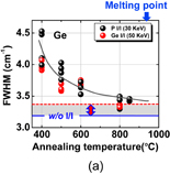
Download figure:
Standard image High-resolution image
Fig. 94. FWHMs in Raman spectra of both (a) Ge with P or Ge ion implantation and (b) Si with P ion implantation are plotted as a function of annealing temperature. That in Ge is not recovered to the initial value even after 800 °C annealing, while that in Si is almost back to the bare wafer quality. Note that the melting temperature of Ge is ∼940 °C.168)
Download figure:
Standard image High-resolution image
Fig. 95. Depth profile of activated electron concentration in laser-thermal-annealed P-implanted Ge. The very high activation of P in Ge is feasible using the non-equilibrium thermal process.173) Reprinted with permission from Ref. 173. © 2014 IEEE.
Download figure:
Standard image High-resolution imageNext, let us discuss a slightly different method, the "snowplow" effect in Ge, to realize low-temperature dopant activation. The snowplow was studied in Si process technology many years ago.174) Dopants implanted into Si were segregated like a "snowplow" and activated at the silicide/Si interface through the silicide formation process at a relatively low temperature. We studied the snowplow process of phosphorus (P) in Ge.175) Ni was used as the germanide metal from the viewpoints of a low reaction temperature with Ge and the low resistivity (∼22 µΩ·cm) of its germanide (NiGe).176) The germanide reaction was carried out in N2 at temperatures ranging from 200 to 500 °C. XRD patterns showed Ni or Ni5Ge3 phases at 200 °C and a well-crystallized NiGe phase above 300 °C. The schematic images of the snowplow process are shown in Fig. 96(a). P ions were implanted with the acceleration voltage of 50 kV and the dose of 1 × 10¹⁵/cm2. A 50-nm-thick Ni film was deposited in UHV, and then Ge substrates were thermally annealed in N2. Ni (including NiGe)/Ge junctions without P ion implantation, of course, showed the Schottky characteristic on n-Ge and an the ohmic one on p-Ge, respectively. Figures 96(b) and 96(c) show that the transition from a rectified I–V to an ohmic one on n-Ge substrate is observed between 200 and 300 °C. Note that the germanide reaction actually lowers the P activation temperature in Ge to 300 °C. Although we found the low-temperature activation of phosphorus experimentally, we did not verify the phosphorus profile. Later, it was reported that the phosphorus pile-up was not observed clearly.177) As a result, the snowplow was effective to lower the activation temperature, but it might not be efficient to enhance the doping density.
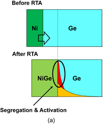
Download figure:
Standard image High-resolution image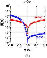
Download figure:
Standard image High-resolution image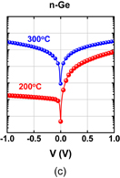
Fig. 96. (a) Schematic image of the snowplow process in NiGe/Ge contact. Dopants are expected to be activated and segregated simultaneously with NiGe solid-phase crystallization. I–V characteristics of P-implanted Ni/Ge junctions after annealing at 200 and 300 °C for (b) p-Ge and (c) n-Ge. Low-temperature activation was clearly demonstrated at 300 °C. This is thanks to the lower temperature crystallization with the help of metal.175)
Download figure:
Standard image High-resolution imageHere, we would like to report another aspect of the junction leakage current in Ge. The lateral leakage path along the peripheral area is generally a concern due to the poor interface passivation and/or electric field enhancement, as schematically shown in Fig. 97. Considering the lateral leakage in addition to the water etching of GeO2, we have so far employed Y2O3 passivation around the contact area in the FET fabrication process. Here, we discuss the passivation-layer dependence of n+/p junction leakage currents in more detail. Three kinds of passivation layers — SiO2, Y2O3, and YGO — were investigated. In the gate stack, the YGO/Ge interface is the best of the three. GeO2 was not investigated because it was easily etched by the wet process. Figure 98 shows the leakage current histogram for n+/p junctions with three passivation layers. For circular junctions with 100 and 200 µm in diameter, the leakage current at junctions passivated by YGO is considerably lower than those of the others. This is quite reasonable when considering the gate stack properties, but it is surprising that the leakage current is strongly dependent on the peripheral passivation.178) Conversely speaking, we can reduce the junction leakage current more by taking care of the peripheral passivation. We have actually achieved the on/off current ratio of more than 106, at |V| = 1 V at the n+/p junction. Therefore, most of rather high junction leakage currents reported so far are not intrinsic but mainly result from the poor peripheral passivation. By optimizing doping and annealing processes in addition to paying attention to the lateral passivation scheme, the leakage current can be reduced much further.
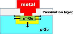
Fig. 97. Schematic description of leakage current path at a planar n+/p Ge junction. It is a serious concern in Ge that the lateral leakage current is related to the passivation layer around the junction, because an interface of the passivation layer with Ge is poorly controllable.
Download figure:
Standard image High-resolution image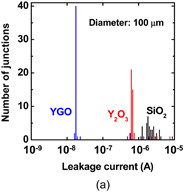
Download figure:
Standard image High-resolution image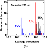
Fig. 98. Histogram of junction leakage currents at Vrev = 1 V, where the junctions are passivated by YGO, Y2O3, and SiO2. Circular junctions with diameters of (a) 100 and (b) 200 µm were used. In case of YGO, the leakage current is significantly lower with a tighter distribution.178)
Download figure:
Standard image High-resolution imageIt is interesting to see that the junction leakage issue includes the same technical challenge as gate stacks and that YGO solves both challenges. In the Si technology, the passivation and gate stacks are automatically satisfied with SiO2. This is a great point of the SiO2/Si system now after all.
7. Setting new devices
In the final section, we would rather introduce new types of Ge FETs than discuss conventional miniaturized MOSFETs. Each operation principle, however, is not new but already known except Sect. 7.4. Electron devices either taking advantages of Ge or compensating disadvantages of Ge are discussed.
7.1. ET-GeOI FET
Extremely thin Ge on insulator (ET-GeOI)179) is analogous to ET-SOI180) in Si technology, and is rather promising, thanks to the junction leakage reduction as well as the DIBL suppression from the device structure viewpoint. We investigated electron and hole mobilities in the front and back channels in GeOI MOSFETs.181) The starting substrate was a 100-nm-thick Ge(100) GeOI wafer with a very low doping (ND < 1 × 1014 cm−2) fabricated by the Smart Cut™ technology on SiO2/Si. 20-nm-thick Y2O3 was deposited by rf-sputtering, and phosphorus was implanted through the Y2O3 layer for the S/D formation. The two-step oxidation (HPO-LOA) of Y2O3 was employed for the gate stack formation. The gate stack structure is schematically shown in Fig. 99(a). The interface layer was not pure GeO2 but Y-doped GeO2. The Ge thickness was thinned down to 9 nm, as shown by the cross-sectional TEM image in Fig. 99(b). Figures 100(a) and 100(b) show well-behaved transfer characteristics (IDS–VGS) of 9-nm-thick GeOI n- and p-MOSFETs under VBG = 0 V. The off leakage currents are well suppressed as expected. The peak electron mobility in a 9-nm-thick GeOI n-MOSFET was 254 cm2 V−1 s−1, which is considerably lower than expected. Figures 101(a) and 101(b) show the Ge thickness dependences of electron and hole mobilities at Ns = 1 × 1012 cm−2 for both the front and back channels of GeOI n- and p-MOSFETs. The electron mobility at the front channel (GeO2/Ge interface) decreases monotonically with the reduction in Ge thickness and drops sharply between 45 and 25 nm of Ge thickness, while the back channel (Ge/SiO2 interface) shows the very low mobility even for thick GeOI cases. In case of hole mobility, the same trend is observed but it is much more moderate.181)
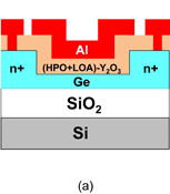
Download figure:
Standard image High-resolution image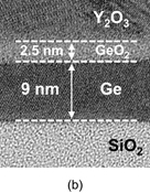
Fig. 99. (a) Schematic view of GeOI MOSFET with raised S/D structures. (b) Cross-sectional TEM image of 9-nm-thick GeOI MOSFET channel. The interface layer was actually Y-doped GeO2, which enabled to achieve a good front interface on thin Ge.181)
Download figure:
Standard image High-resolution image
Download figure:
Standard image High-resolution image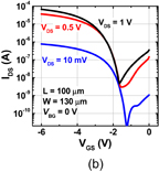
Fig. 100. IDS–VGS of 9-nm-thick GeOI (a) n- and (b) p-MOSFETs with a channel width/length of 130 µm/100 µm under VBG = 0 V. A higher work function metal than Al is needed for gate electrode to adjust both Vth values in both n- and p-MOSFETs, although the leakage currents are well suppressed.181)
Download figure:
Standard image High-resolution image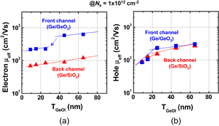
Fig. 101. Ge thickness dependence of (a) electron and (b) hole mobilities at the front (GeO2/Ge interface) and back channels (SiO2/Ge interface) at Ns = 1 × 1012 cm−2 in GeOI MOSFETs. Below 40-nm-thick Ge, the electron mobility at the front channel is more significantly degraded than the hole mobility, and approaches the back channel value. It should be attributable to the back Ge/SiO2 interface.181)
Download figure:
Standard image High-resolution imageThe front channel mobility degradation clearly comes from the poor back interface of the Ge channel on SiO2. It is also clear that the Ge crystallinity is also very poor near the back interface (Ge/SiO2). Thus, "back interface-aware" GeOI fabrication (bonding process and/or Ge-friendly BOX material) will be required for high-performance GeOI devices. We hope that it will be possible because the gate stack technology has been dramatically improved by taking care of the Ge interface, as discussed in Sects. 2 and 3. Very recently, Yu et al. have demonstrated 3-nm-thick GeOI FET operation by taking special care of the back interface.182) Although the mobility is still not high, this work suggests that ET-GeOI FETs are potentially promising for the scaling by optimizing the back interface from the process and material viewpoints. Note that this consideration is also applicable for the local Ge channel. In case of Ge FinFETs, this optimization will not be a problem because both front and back interfaces are gate stack channels. The Ge condensation method is completely different GeOI preparation technique from the Smart Cut™ process. Those who are interested in this technique should see Refs. 183 and 184.
7.2. Metal source/drain FET
To reduce the parasitic resistance in source and drain regions, metal source/drain FET has long been investigated in Si. Since the Schottky barrier height is a key parameter for designing the device, the almost perfect FLP at the metal/Ge interface has been negatively considered for n-MOSFETs, while in case of p-MOSFETs in Ge, it is rather easy to make metal source/drain MOSFET on Ge185) because any metal can make an ohmic contact with p-Ge.
As discussed in Sect. 6.1, we know that the FLP on Ge is alleviated by inserting UTO between metal and Ge. Therefore, we applied this interface engineering method in the fabrication of metal source/drains for Ge n-MOSFETs on p-Ge.140) Figures 102(a) and 102(b) show a schematic view of fabricated Al source/drain Ge n-MOSFET and the cross-sectional TEM image of the tunnel contact at the Al/p-Ge interface. About 2-nm-thick GeO2 was formed on a p-Ge substrate to achieve an ohmic contact between the Al source/drain and the electron inversion channel of Ge. As shown in Fig. 102(c), IS–VDS characteristics in the low-VDS region indicate a very low parasitic resistance despite the absence of n-type impurity doping in the source region. Considering a low solubility of dopants in Ge, metal source/drain FET is a plausible candidate for the ultrashort-channel Ge FET in which the fringing field works more effectively.186) The present demonstration was carried out on the bulk Ge substrate, but it is obviously more favorable to fabricate on GeOI in terms of the leakage current reduction. Yamamoto et al. have recently demonstrated metal source/drain n- and p-MOSFETs using TiN contact.187) As discussed in Sect. 6.1, several methods have been reported to enable the metal contact to the n-Ge substrate ohmic. Thus, ultra-short channel metal source/drain n-channel Ge FETs will be more elegantly demonstrated.

Download figure:
Standard image High-resolution image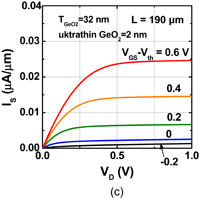
Fig. 102. (a) Schematic cross-sectional image of metal source/drain Ge n-MOSFET with Al/ultrathin (∼2 nm) GeO2/Ge junction without any doping. (b) Cross-sectional TEM image of Al/ultrathin GeO2/Ge junction. (c) IS–VDS characteristics in metal source/drain Ge n-MOSFET depicted in (a). The gate oxide was 32-nm-thick GeO2. A large parasitic resistance, which is often seen in metal/sotuce/drain FETs at a small VDS region, is not observed.140)
Download figure:
Standard image High-resolution image7.3. Junctionless FET
Junctionless (JL) FETs using Si nanowire FETs were proposed. The device image and operation principle are schematically shown in Fig. 103(a)188) and Fig. 3(b),189) respectively. JL-FETs have the advantages that no source/drain (S/D) formation is needed and that carrier transport is less sensitive to the channel interface. Simulations-based analysis for JL-FETs have been carried out by many researchers.190,191)
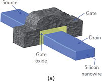
Download figure:
Standard image High-resolution image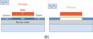
Fig. 103. (a) Schematic view of a junctionless nanowire transistor.188) (Adapted by permission from Macmillan Publishing Ltd.) (b) Operation principle in n-type junctionless FETs.189) (Adapted by permission from Macmillan Publishing Ltd.)
Download figure:
Standard image High-resolution imageWe tried to make JL-FETs on Ge. A heavily doped p-type GeOI wafer with 100-nm-thick buried SiO2 was used for p-channel Ge JL-FET. The SIMS analysis showed that the p-type dopant concentration was around 1019 cm−3. Mesa-type Ge islands were defined by wet etching and substrate Si was used as the back-gate electrode. As the Ge thickness was decreased to less than 30 nm, the drain current was modulated by the back-gate bias as shown in Figs. 104(a) and 104(b).192) The Ion/Ioff ratio of a device on 11-nm-thick Ge was larger than 104 at VGS between −40 and 40 V. The JL-FET channel is a resistor in case without the gate voltage, while the majority carriers (holes) flow through the Ge layer under a negative VGS. When a positive VGS is applied, holes are electrostatically depleted and drain current decreases. Therefore the depletion layer width is a critical parameter for JL-FETs to achieve the off-state. The maximum depletion layer width of Ge with an impurity concentration of 1019 cm−3 is estimated to be about 11 nm, considering the dielectric constant and intrinsic carrier concentration of Ge to be 16 and 2.4 × 1013 cm−3 at room temperature, respectively. The output characteristics of the 11-nm-thick Ge JL-FET are shown in Fig. 104(c). The effective mobility of 11-nm-thick Ge JL-FETs was roughly 100 cm2 V−1 s−1 and not sensitive to the gate bias, while in conventional inversion-mode MOSFETs the minority carriers are accumulated at the semiconductor/insulator interface and the carrier mobility is sensitive to the interface. Furthermore, since in case of p-channel Ge JL-FETs, all metals make ohmic contacts with p-Ge, it is favorably considered that the contact resistance in p-channel Ge JL-MOSFETs is not affected by the unexpected doping density fluctuation in Ge. The results have obviously been much improved by employing double-gated JL-FETs.193)
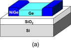
Download figure:
Standard image High-resolution image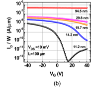
Download figure:
Standard image High-resolution image
Fig. 104. (a) Schematic image of junctionless Ge p-FET structure with NiGe source/drain, and (b) IDS–VGS characteristics of the junctionless Ge p-FET, with Ge thickness as a parameter. IDS is modulated by the back gate bias in below 15-nm-thick Ge with a doping concentration of about 1019 cm−3. (c) IDS–VDS characteristics of the Ge junctionless p-FET fabricated on 11-nm-thick heavily doped GeOI substrate.192)
Download figure:
Standard image High-resolution imageWe expect that Ge JL-FETs should show better performance than Si one because of the less coulombic scattering due to the higher dielectric constant of Ge. This beneficial point of Ge in the carrier mobility is more significant in the more heavily doped region. Concerning n-channel Ge JL-FETs, it is worthwhile mentioning that the electron mobility in bulk n-Ge (1000 cm2 V−1 s−1) is one order of magnitude higher than that in n-Si (100 cm2 V−1 s−1) with Nsub = 1019 cm−3. Thus, n-channel JL-FETs on Ge will be much more attractive than those on Si from the mobility enhancement viewpoint. As a matter of fact, Si JL-FETs on heavily doped SOI have shown a substantially low mobility because of the significant Coulomb scattering. Figure 105 clearly shows a significant advantage of heavily doped Ge, in which an enhancement of the bulk electron mobility ratio, μGe/μSi was calculated using the following equation based on the Brooks–Herring model for the Coulomb scattering.194)
in which βBH is the Brooks–Herring parameter.

Fig. 105. Electron mobility ratio of Ge to Si as a function of donor concentration calculated using the Brooks–Herring model.194) Since the dielectric constant of Ge is higher than that of Si, the electron mobility in Ge is more advantageous than that in Si with the doping concentration higher than 1018 cm−3. In fact, the electron mobility in Ge with a high donor concentration is significantly higher than that in Si.89)
Download figure:
Standard image High-resolution imageFigure 106 shows well-behaved output characteristics of n-channel Ge JL-FET with 15-nm-thick Ge. The electron mobility, however, is rather low (100–200 cm2 V−1 s−1), which is probably due to the fact that electrons may be more sensitive to the poor interface Ge quality than expected. Nevertheless, the mobility with 34-nm-thick Ge was actually increased to ∼800 cm2 V−1 s−1,195) although the off-state leakage current was poor. It suggests that further interface control in the Ge channel will enable to achieve high performance Ge JL-FETs by making the best of highly doped Ge advantages.
Fig. 106. IDS–VDS characteristics of 15-nm-thick n-channel Ge junctionless FET. The electron mobility is not so high (∼150 cm2 V−1 s−1), possibly due to the poor back interface in the present stage. In fact, a thicker Ge film showed a much higher mobility (∼800 cm2 V−1 s−1), although the off-state leakage current was not negligible.195)
Download figure:
Standard image High-resolution image7.4. New field effect on Ge
Heavily doped semiconductors are now used not only for source/drain but also for the JL-FET channels discussed previously. Meanwhile, it is well known that the heavy doping of impurities may modify semiconductor properties such as the energy band gap narrowing196) and the elastic constant modulation.197) These phenomena were studied several decades ago experimentally and theoretically. It is, however, still difficult to discriminate between free carrier and dopant effects. We paid attention to the fact that a back-gated GeOI FET could be used for separating the free-carrier effect from the dopant one. Optical analyses are actually available from the top surface of GeOI FETs under the back bias application, which can only change the carrier density.
Bottom-gated FETs on lightly doped GeOI wafers were fabricated with Y2O3 passivation on the top surface, which could reduce non-radiative surface recombination.198) The schematic image is shown in Fig. 107. In Fig. 108, the Raman shift in the GeOI FET is clearly seen to the lower wave number in the negative back bias (hole accumulation), while it does not change in the positive one (electron accumulation).199) Furthermore, since the FWHM of the Raman spectra does not change at all even in the hole accumulation (data not shown), the Raman shift will not be due to the so called Fano effect, which has often been discussed for explaining the Raman shift in heavily doped semiconductors.200)

Fig. 107. Experimental setup for microscopic Raman (λ = 488 nm) and PL (λ = 457 nm) measurements under a finite back-gate bias to Si substrate. The Ge surface was passivated with Y2O3 to reduce the surface recombination (nonradiative process).198) The laser beam diameter was 2 µm.
Download figure:
Standard image High-resolution image
Fig. 108. Back-gate bias dependences of Raman peak position and drain current in 11-nm-thick GeOI FET. Ge was undoped. Phonon softening is clearly observed only in the negative back bias (hole accumulation).199)
Download figure:
Standard image High-resolution imageMicroscopic photoluminescence (PL) measurements were also carried out in the same sample as a function of carrier density with a fixed dopant density. PL peak positions in GeOI FETs are shown in Fig. 109 together with the drain current.201) The PL peak position shifts to a lower energy with the increase in the number of free carriers of both polarities. This experiment enables us to characterize the free carrier effect on the energy band gap narrowing under a fixed dopant density. To our knowledge, this is the first observation that only free carriers can change the optical phonon at the Γ-point and energy band gap.
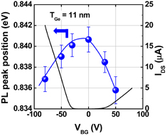
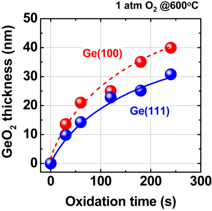
Fig. 109. Back-gate bias dependences of PL peak energy and drain current in 11-nm-thick GeOI FET. Energy band gap narrowing is clearly observed both under the negative (hole accumulation) and positive (electron accumulation) back bias conditions, which is in striking contrast to the Raman results shown in Fig. 108.201)
Download figure:
Standard image High-resolution image
Free carrier effects on both Raman and PL results may be intuitively understandable by considering the covalent bonding of two atoms under variable carrier density.201) The results presented here may be evidence that the rigid phonon and rigid energy band gap models are more or less violated in the highly carrier-accumulated region in Ge.202) Although a more quantitative analysis will be needed to understand free carrier effects, new applications such as field-effect photonic devices might hopefully be invented.
8. Conclusions and future outlook
If Ge FETs have intrinsic challenges that we cannot overcome in gate stack and contact formations, we have to abandon Ge CMOS. We think, however, that most of them have already been solved as described in this review, although many technical challenges remain to be tackled.
The poor electron mobility in n-channel Ge FETs is not intrinsic. We can engineer the Ge interface through the understanding of thermodynamics and kinetics for controlling the Ge interface. Now, ∼2,000 cm2 V−1 s−1 as the highest peak electron mobility has been demonstrated on the simple planar FETs. This mobility value is almost half as high as that of the bulk Ge. GeO2/Ge gate stacks and then high-k/Ge ones have been investigated. The excellent performance of gate stacks with EOT = 0.5 nm has been demonstrated.
Furthermore, we have emphasized the importance of the network stability for controlling the gate stack reliability and proposed a concept of the "rigidity" of dielectric films because we think that the network strength may be more important than single-bond robustness. We are not trying to obtain zero defects but as few as possible. We have concluded that initially good gate stacks do not necessarily mean good ones in terms of the long-term reliability. Thus, we have regrettably judged that GeO2/Ge gate stacks would not satisfy practical reliability requirements. We think that the rigidity concept will be very useful for understanding other gate stack systems, although more systematic data are, of course, needed for estimating the reliability quantitatively.
Concerning the Fermi level pinning at the metal/Ge interfaces, almost perfect pinning is not completely but considerably alleviated, and even the ohmic contact is available for metal/n-Ge interfaces without any doping. Furthermore, a new view of the Fermi level pinning on Ge has been discussed on the basis of reconsideration of the metal-induced gap states model. It seems reasonable experimentally, though it should be validated theoretically. We hope the guideline discussed in this paper will be helpful for the contact design on new channel materials as well.
As discussed through this review, we are very sure that Ge FETs are quite promising not only for p-channel but also for n-channel FETs. Advanced Ge FinFETs203) and Ge CMOS ring oscillator operation204) have been reported recently. This is good news for Ge CMOS technology.
Performance boosters such as the mechanical strain on Ge205,206) have not been discussed in this review, nor has Ge–Sn, which is now under intensive investigation from the viewpoints of both electronics205,207) and photonics.208–210) The Ge avalanche photodetector for on-chip optical interconnects is an interesting application in terms of a fusion of electronics and photonics.211) Furthermore, there are a number of other important and interesting issues to discuss, such as low-temperature Ge crystallization for 3D integration or high-performance Ge thin-film transistor (TFT) technology.212–214) We know that many issues remain for further work, but we hope that versatile applications of Ge derived from material understanding will be extended successfully. It will be fantastic and exciting.
Finally, we would like to conclude by saying "be more positive about Ge CMOS".
Acknowledgements
We would like to thank our colleagues (K. Kita, K. Nagashio, and T. Yajima), and former Ph.D. students and postdoctoral fellows (S. K. Wang, C. H. Lee, T. Tabata, C. Lu, S. Kabuyanagi, D. D. Zhao, W. F. Zhang, and T. C. Liu) at The University of Tokyo for their great contributions to the understanding and engineering of Ge technology. We would also like to thank S. Yamaguchi for his critical comments and helpful suggestions on the atom diffusion kinetics in oxides. This work was mainly supported by JST-CREST, and we would like to thank its supervisor, H. Watanabe, for his helpful guidance. It was also partly supported by JSPS-KAKENHI (Kiban-S and Kiban-A) and partly in collaboration with STARC.
Biographies

Akira Toriumi received the B.S. degree in physics, the M.S. and Ph.D. degrees in applied physics from The University of Tokyo in Japan, 1978, 1980, and 1983, respectively. He joined R&D Center of Toshiba Corporation in 1983. In May 2000, he moved to The University of Tokyo. His research interests have been on semiconductor device physics and related materials science throughout his professional carrier. He is currently studying materials science of high-k dielectrics, and physics and technology of germanium CMOS as well as functional oxides. He is a JSAP and IEEE Fellow.

Tomonori Nishimura received the B.E. and M.E. degrees in material physics from Osaka University in 1998 and 2000, and Ph.D. degree in material engineering from The University of Tokyo in 2017, respectively. He is currently studying gate stacks and metal/Ge contact for high performance Ge CMOS. He is a member of the Japan Society of Applied Physics and the IEEE Electron Device Society.