
Abstract
4H-SiC lateral double implanted metal–oxide–semiconductor field effect transistors (LDIMOSFET) were fabricated on on-axis semi-insulating SiC substrates without using an epi-layer. The LDIMOSFET adopted a current path layer (CPL), which was formed by ion-implantation. The CPL works as a drift region between gate and drain. By using on-axis semi-insulating substrate and optimized CPL parameters, breakdown voltage (BV) of 1093 V and specific on-resistance (Ron,sp) of 89.8 mΩ·cm2 were obtained in devices with 20 µm long CPL. Experimentally extracted field-effect channel mobility was 21.7 cm2·V−1·s−1 and the figure-of-merit (BV2/Ron,sp) was 13.3 MW/cm2.
Export citation and abstract BibTeX RIS

Content from this work may be used under the terms of the Creative Commons Attribution 4.0 license. Any further distribution of this work must maintain attribution to the author(s) and the title of the work, journal citation and DOI.
Silicon carbide (SiC) is an attractive material for high power devices due to high mobility and high breakdown electric field.1,2) A number of vertical high voltage devices such as SiC double-implanted MOSFET (DMOSFETs) and U-shaped MOSFET (UMOSFETs), have been demonstrated.3–6) In contrast, not many lateral SiC devices have been investigated, in comparison with the vertical devices.7–10) Recently, there has been increased demand for the lateral devices, to implement both high voltage power device and low-voltage circuits on a single chip.11)
In general, lateral SiC MOSFETs are fabricated on a SiC epi-layer which was grown on off-axis conducting substrates. For 4H-SiC, 4°-off toward  substrate is widely used in order to avoid poly-type inclusion.12) However, step bunching often occurs during the epitaxial growth and high temperature activation process.13) The step bunching makes surface rough14) and causes scattering of carriers at the surface. Consequently, the channel mobility of the MOSFET is dramatically reduced.15,16) Therefore, on-axis wafer has advantages for improving current characteristics compared to the off-axis wafer.
However, it is still possible to create poly-type defects on an on-axis wafer during epitaxial growth, and elimination of the epi-layer is preferred in many aspects.17) In this paper, 4H-SiC lateral double implanted MOSFET (LDIMOSFET) have been designed and fabricated on an on-axis high purity semi-insulating (HPSI) substrate. In order to avoid the problems mentioned above, we used the on-axis SiC substrate. Our devices showed similar static characteristics comparable to those of the conventional devices.
Figure 1 shows a cross-sectional view of our device. We simulated the static characteristics by using a device simulator Silvaco-ATLAS. As shown in the figure, the proposed device adopted a current path layer (CPL) instead of an epi-layer used in the conventional device. The CPL region is formed by ion-implantation. N+ and p regions in the figure are also realized by ion implantation. The CPL region plays an important role in obtaining MOSFET characteristics. At a forward bias condition, the CPL serves as a current path, and at reverse bias it serves to support the breakdown voltage. Without the CPL region, only the semi-insulating layer exists between the p-base and n+ drain of the device. In this case the forward current will be very small, due to a low carrier density in the semi-insulating substrate.

Fig. 1. Cross-sectional view of the lateral double implanted MOSFET.
Download figure:
Standard image High-resolution imageIt is important to optimize the CPL parameters (doping concentration and depth), in order to obtain desired forward and reverse characteristics. For optimization, device simulation was performed by using Silvaco-ATLAS. Simulations were performed by varying the doping concentration (NCPL), depth (DCPL), and length (LCPL) of the CPL region. The doping concentrations of p-base and n+ source/drain were fixed at 2.5 × 10¹⁷/cm3 and 8 × 10¹⁹/cm3, respectively. A channel length of 2 µm and a gate oxide thickness of 55 nm were used. Device parameters used in the simulation are shown in Table I.
Table I. Device parameters used in simulation.
| Doping conc. (/cm3) | Depth or length (µm) | |
|---|---|---|
| P-base region | 2.5 × 10¹⁷ | Depth: 0.6 |
| Sourced/drain region | 8 × 10¹⁹ | Depth: 0.3 |
| CPL region | 1 × 10¹⁵–1 × 10¹⁷ | Length: 5–20 |
| Depth: 0.1–0.4 | ||
| Semi-insulating substrate | <109 | — |
Figure 2 shows the simulated characteristics (breakdown voltage and specific on-resistance) of the proposed device as a function of NCPL and DCPL. In this figure, LCPL was fixed at 5 µm. When DCPL varies from 0.1 to 0.4 µm in Fig. 2, the device exhibited breakdown voltages of 210–615 V. When the NCPL and DCPL were increased, the breakdown voltages decreased. Especially, when NCPL > 4 × 10¹⁶/cm3 and DCPL > 0.3 µm, breakdown voltages sharply decreased. At a given doping density of NCPL, an increase of the depth (DCPL) encourages the electric field in the depletion layer to have a triangular shape, and the maximum electric field becomes higher. This explains the lower breakdown voltages as DCPL increases.

Fig. 2. Simulated breakdown characteristics and specific on-resistance (LCPL = 5 µm).
Download figure:
Standard image High-resolution imageFigure 3 shows surface electric field distributions in the devices with DCPL of 0.1 and 0.4 µm, simulated at VDrain = 300 V. As shown in the figure, depletion layer of the device with DCPL = 0.4 µm does not reach the drain, and the maximum electric field is higher. As shown in Fig. 2, specific on-resistance increases significantly when NCPL is lower than 2 × 10¹⁶/cm3. Therefore, in order to obtain high breakdown voltage and low specific on-resistance, NCPL and DCPL should be within range of 2 × 10¹⁶ ≤ NCPL ≤ 4 × 10¹⁶/cm3 and 0.2 ≤ DCPL ≤ 0.3 µm, respectively. For device fabrication, considering the simulation results, we used NCPL = 2 × 10¹⁶/cm3, and DCPL = 0.3 µm, respectively.
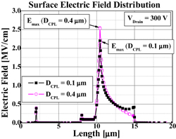
Fig. 3. Simulated surface electric field distribution at VDrain = 300 V.
Download figure:
Standard image High-resolution imageWe fabricated the LDIMOSFET devices using parameters discussed above. For device fabrication, on-axis HPSI 4H-SiC wafers were used. High temperature (500 °C) multiple implantations of aluminum (Al+) and nitrogen (N) were carried out to obtain p-base, n+ source/drain, and CPL regions. For the p-base region, Al+ implantation was performed at 0.6 µm depth with 2.73 × 10¹³/cm2 dose. For the CPL region, N implantation was used at 0.3 µm depth with dose of 3.38 × 10¹²/cm2. Ion implantation for ohmic contacts were performed with doses of 2.81 × 10¹⁵/cm2 and 2.38 × 10¹⁵/cm2 for n-source/drain (N/N+) and p-source (Al/P+), respectively. Doses for each region were chosen by considering the activation ratio of the HPSI substrate (N: 25.2%, Al: 27.9%, which was verified by experiments) and concentration degradation due to the deep traps within HPSI substrate.18) The expected NCPL and DCPL of the CPL region are 2 × 10¹⁶/cm3 and 0.3 µm, respectively.
LCPL was varied from 5 to 20 µm. A 55-nm-thick gate oxide was thermally grown followed by NO treatment. After that, 700-nm-thick n+ polysilicon is deposited for the gate electrodes. Then a 200-nm-thick SiO2 passivation layer was deposited. After the passivation, Ni-silicide for ohmic contact was formed and annealed at 950 °C for 90 s. Finally, a pad metal was deposited for electrodes. The contact resistance of silicide n+ source and drain was 6 × 10⁻⁵ Ω·cm2. To clarify the effect of the CPL region, LDIMOSFET without a CPL region was also fabricated.
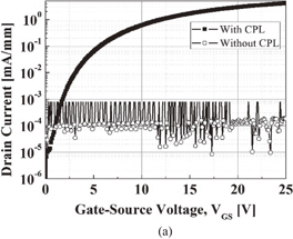
Figure 4 shows current characteristics of the device measured at VDrain = 1 V (LCPL = 5 µm, WChannel = 150 µm). This figure shows that only the device with CPL functions as a transistor. The maximum transconductance (gm) of the device is 0.244 mS/mm. The extracted channel mobility of the device at the maximum transconductance is 21.7 cm2·V−1·s−1. The reported mobility range of the Al-implanted MOSFETs fabricated on the 8° off-axis epitaxial layer is 6 to 9 cm2·V−1·s−1.19) In contrast, mobility range of the Al-implanted MOSFET fabricated on the on-axis epitaxial layer is 9 to 19 cm2·V−1·s−1, and they explain that the mobility increase is due to the lower surface roughness. In our device, we used on-axis substrate to avoid the surface roughness scattering caused by the step bunching and we observed mobility comparable to those measured in the device implemented on the epitaxial layer grown on the on-axis wafer. This results suggests that our mobility increase is related to the lower surface roughness in the on-axis substrate.
Download figure:
Standard image High-resolution image
Fig. 4. Drain currents (a) and transconductances (b) as a function of gate voltages. Currents measured in two devices (with and without a current path layer) are compared.
Download figure:
Standard image High-resolution imageThe extracted threshold voltage of the device by using the gm-max method is 7 V. The device without CPL shows very low drain current, due to the highly resistive drift region. There are considerable amount of intrinsic deep traps such as Z1/2 and EH6/7 in the semi-insulating substrate,20,21) which removes free carriers in the device without CPL. Figure 4 shows that CPL can replace the epi-layer in the LDIMOSFET structure.
Figure 5 shows measured drain currents as a function of drain voltage. The device with CPL shows transistor characteristics (LCPL = 5 µm). Gate voltage was changed from 0 to 25 V with 5 V increment. In the figure, the highest drain current is 22 mA/mm. Although the current flow is restricted to a thin layer (0.3 µm depth), the device exhibits large current due to the high carrier concentration in the CPL. Currents in the device without CPL slightly increase when drain voltage exceeds 10 V. This small increase of current comes from the drift flow of electrons due to the high electric field between p-base and n+ drain. A specific on-resistance of the device 17.2 mΩ·cm2 at VG = 25 V and VD = 1 V. When the LCPL was increased from 5 to 20 µm, the specific resistance of the device also increased, from 17.2 to 89.8 mΩ·cm2.

Fig. 5. Drain currents as a function of drain voltages. Currents were measured in two devices (with and without a current path layer).
Download figure:
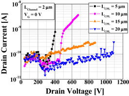
Standard image High-resolution imageThe maximum breakdown voltage of a conventional lateral device implemented on conducting substrate is determined by the thickness and doping concentration of the epi-layer. Thick lightly doped epi-layer under the drift region is required to prevent breakdown in the vertical direction.22) In other words, breakdown voltage is limited by the depletion in the vertical direction. In our device, epi-layer and drift region of the conventional device is replaced by semi-insulating substrate and CPL region. Because the doping concentration of the semi-insulating substrate is extremely low, maximum breakdown voltage of the device is determined by the depletion in the CPL region. Therefore, breakdown voltage of our device depends on LCPL, DCPL, and NCPL. The measured breakdown voltages for different LCPL are shown in Fig. 6. The current shows a sharp rise at high drain voltages, and we define this voltage as the breakdown voltage.
Fig. 6. Breakdown characteristics measured in devices with different lengths of current path layer (LCPL).
Download figure:
Standard image High-resolution image
As shown in the figure, longer LCPL shows higher breakdown voltage, and the maximum voltage of 1093 V was observed in the device with LCPL = 20 µm. The observed breakdown voltages show almost linear dependence on LCPL, and this suggests that the whole CPL regions are depleted in this configuration. Our simulation results also confirmed that entire region of CPL was depleted, even in the device with LCPL = 20 µm.
Maximum breakdown voltage (BV) of 1093 V was achieved with low specific on-resistance (Ron,sp) of 89.8 mΩ·cm2 at LCPL = 20 µm. The figure of merit (BV2/Ron,sp) of the fabricated device in this paper is 13.3 MW/cm2. The breakdown voltage of the fabricated device can be improved by using a field plate. Due to the two-dimensional effects at the bottom corner of the p-base and n+ drain, field crowding occurs at the edges leading to the field spikes, and the breakdown voltage is reduced as a result. This can be avoided by using field plates placed on top of the gate and drain.
The specific on-resistance of the device can be improved by adopting the RESURF principle.23,24) Parameters for the full depletion with higher doping in the CPL region can be found by the simulation. The effect of the field plates and RESURF principle is under investigation.
In conclusion, 4H-SiC LDIMOSFET have been designed and fabricated on on-axis HPSI substrate without using an epi-layer. We confirmed that the CPL could replace the epi-layer of the conventional device, without sacrificing their performance. Measured effective channel mobility of 21.7 cm2·V−1·s−1 was obtained, and high breakdown voltage and low specific on-resistance were achieved. Our device exhibited a specific on-resistance of 89.8 mΩ·cm2 with a threshold voltage of 7 V, when LCPL = 20 µm. The measured maximum breakdown voltage was 1093 V, yielding a figure of merit (BV2/Ron,sp) of 13.3 MW/cm2. These results show that 4H-SiC LDIMOSFET fabricated on a semi-insulating substrate without an epi-layer is a prospective candidate for power integrated circuits.
Acknowledgement
This research was supported by Korea Electrotechnology Research Institute (KERI) Primary research program through the National Research Council of Science and Technology (NST) funded by the Ministry of Science, ICT and Future Planning (MSIP) (No. 17-12-N0101-11).