
Abstract
A process for the simultaneous fabrication of microcavity structures on both sides of a film was proposed and demonstrated to develop a free-standing-type integrated absorber–emitter for use in solar thermophotovoltaic power generation systems. The absorber–emitter-integrated film comprised a heat-resistant Ni–W alloy deposited by electroplating. A two-step silicon mould was fabricated using deep reactive-ion etching and electron beam lithography. Cavity arrays with different unit sizes were successfully fabricated on both sides of the film; these arrays are suitable for use as a solar spectrum absorber and an infrared-selective emitter. Their emissivity spectra were characterised through UV–vis–NIR and Fourier transform infrared spectroscopy.
Export citation and abstract BibTeX RIS

Content from this work may be used under the terms of the Creative Commons Attribution 4.0 license. Any further distribution of this work must maintain attribution to the author(s) and the title of the work, journal citation and DOI.
Solar thermophotovoltaic (STPV) power generation has attracted intensive interest because of its ability to achieve high conversion efficiency beyond the Shockley–Queisser limit1) of conventional photovoltaic cells.2–4) The key component of an STPV system is an integrated absorber–emitter, which comprises a solar light absorber and a wavelength-selective thermal emitter. The former is heated by concentrated, broad-spectrum solar radiation, causing its temperature to increase. This high temperature stimulates the emitter, which radiates a narrow-bandwidth infrared light with a wavelength similar to the band-edge wavelength of the subsequent photovoltaic (PV) cell to maximise the conversion efficiency.5) Therefore, the spectral modification of both the absorbance and emissivity of a material, on the basis of Kirchhoff's law of thermal radiation, is strongly required for both STPV emitter and absorber.6–9)
The high-temperature operation of STPVs requires heat-resistive materials. A microcavity structure formed on a heat-resistive metal surface is one promising approach, and extensive efforts have been dedicated to the development of microcavity fabrication processes, including the fast-atom beam etching of tungsten10) and the selective etching of a Ni-based superalloy.11) However, the integration of a microstructured emitter and absorber is difficult because it requires either the formation of microcavities with different dimensions or a complicated heterointegration process.12)
We have developed a microcavity fabrication method based on the electroplating of heat-resistive Ni–W alloy13–15) on a microstructured silicon mould and its lost moulding.16) Although the integration of an STPV absorber–emitter on a free-standing thin film offers advantages such as reducing the heat capacity and reaching a high temperature within a short time, its fabrication remains challenging. Therefore, in this study, we present a novel method for the simultaneous fabrication of both an absorber and an emitter with different dimensions on opposite sides of a free-standing Ni–W film; this approach considerably simplifies the absorber–emitter integration process. Using two different masks, we prepared a two-stage structured mould on a silicon surface and subsequently used an electroplating method and silicon lost-moulding method to fabricate thin films with different microstructures on opposite sides. In this study, we also include measurements and assessments of the optical characteristics of the fabricated samples.
A rectangular cavity on a flat metal surface has resonant modes, and its wavelengths are given by17)
where l, m, and n are integers ( and
and  ) and Lx, Ly, and Lz denote the size of a microcavity (Lx and Ly are the aperture sizes). In contrast, a periodic array of microcavities with a spoof surface plasmon polariton (SPP) resonant mode at the wavelength is given by18)
where Λ is the period of the array, i and j are integers, and ε is the dielectric function of the metal. By approximating a metal as a perfect conductor, this equation can be simplified to  . The longest wavelength among λlmn and λSPP gives a cutoff wavelength λC, which determines the absorbance spectrum. The absorbance increases when the wavelength is smaller than λC and decreases when the wavelength is larger than λC. The emission regime change is characterised by an aperture ratio AR = LxLy/Λ2. When the AR is high, λlmn determines λC, whereas when the AR is low, λSPP dominates λC.18)
Figure 1 shows a brief description of the fabrication process. As illustrated in Fig. 1(d), microcavities are formed on both sides of the suspended Ni–W film wherein they modify spectral emissivity. The fabrication process is briefly explained as follows: A silicon mould is fabricated as shown in Fig. 1(a). The mould consists of square pillars with different heights, i.e., short square pillars are surrounded by tall pillars. A Ni–W alloy film is electroplated on the mould, and the gaps between pillars are filled by the alloy film, as shown in Fig. 1(b). As a result, a sparse array of large cavities is formed at volumes surrounded by the sidewalls of the tall pillars and the tops of the short pillars. This large cavity can be used as an emitter, and the cavity size can be controlled by adjusting the number of short pillars, the height difference between the tall and the short pillars, and the duration of electroplating. In contrast, a dense array of small cavities is formed on the backside of the Ni–W alloy film after the removal of the silicon mould, as shown in Fig. 1(c). This short cavity can be used as an absorber, and the size of the cavity corresponds to the size of each pillar. With this approach, cavities with different sizes can be formed on both sides of a Ni–W film via a single electroplating deposition, as shown in Fig. 1(d). Light waves with a wavelength substantially longer than λC are reflected by the microcavity-structured surface, whereas light waves with wavelengths shorter than λC are absorbed. To fabricate a solar absorber and selective IR emitter, microcavities on both sides of suspended Ni–W thin films must be carefully designed to achieve effective conversion from broad sunlight to narrow thermal emission.

Fig. 1. Schematic of the process used to fabricate an integrated absorber–emitter.
Download figure:
Standard image High-resolution imageFigure 2 shows the detailed fabrication process of the absorber–emitter. First, a Cr layer of 40 nm thickness was sputtered onto a 2 × 2 cm2 silicon substrate (a). The mask pattern for the tall pillars was created by electron beam lithography (EBL) with a negative EB resist (SAL601-SR7) (b) and Cr etching using an aqueous solution (c). The short pillar pattern was drawn by the second EBL using the same resist (d). The pillars were formed through a two-step deep reactive-ion etching (deep RIE) process (e, f). After the first round of deep RIE, an O2 plasma asher was used to remove the second resist mask and expose the Cr pattern as the mask layer for the second round of deep RIE. Thus, pillars with two different heights were produced. Some residuals produced between deep RIE processes could be removed using SF6 plasma with the RIE apparatus. Scanning electron microscopy (SEM) images of the mould after the aforementioned steps are shown in Fig. 3. Cr and Au were then sputtered onto the mould as a seed layer with thicknesses of 10 and 50 nm, respectively, and a Ni–W alloy was electroplated19,20) (g). After silicon dry etching at the backside using deep RIE and XeF2 gas etching followed by seed layer etching, a film with microstructures on both sides was obtained (h).

Fig. 2. Detailed fabrication process for the integrated absorber–emitter.
Download figure:
Standard image High-resolution image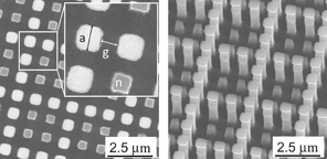
Fig. 3. SEM images of a Si mould.
Download figure:
Standard image High-resolution imageAs shown in Fig. 3, the design parameters of a mould are defined as follows: a is the width of a pillar, h1 and h2 are the heights of the tall and short pillars, t and ts are the thicknesses of the Ni–W layer and seed layers (60 nm), respectively, g denotes the gap spacing between the pillars, and n denotes the number of short pillars between tall pillars. The cavity sizes and periods for both absorbers and emitters are calculated as
Table I shows the design parameters of the pillars, together with the expected longest wavelengths for each regime [λ101 and  ]. For all designs, h1, h2, and (t + ts) were fixed at 7, 2, and 0.5 µm, respectively. Samples A, B, and C have the same absorber cavity dimensions (a and g) and different n values, corresponding to different emitter cavity dimensions L. Samples A and D have identical n values and their a and g parameters are swapped, so they have different emitter cavity dimensions L and identical emitter cavity periods Λ. Therefore, samples A to D are used for emitter characterization. Samples B, E, and F have identical g and n values (g = 0.5 µm and n = 2) and different a values (B: 0.7, E: 0.5, and F: 0.9 µm, respectively), corresponding to different absorber cavity dimensions. Therefore, they are used for absorber characterization.
Table I. Summary of fabricated mould and emitter dimensions.
| Design | a (µm) | g (µm) | n | Absorber | Emitter | ||||
|---|---|---|---|---|---|---|---|---|---|
| AR (%) | λ101 (µm) | λSPP (µm) | AR (%) | λ101 (µm) | λSPP (µm) | ||||
| A | 0.7 | 0.5 | 1 | 47 | 1.6 | 1.2 | 9 | 1.4 | 2.4 |
| B | 0.7 | 0.5 | 2 | 47 | 1.6 | 1.2 | 28 | 3.7 | 3.6 |
| C | 0.7 | 0.5 | 3 | 47 | 1.6 | 1.2 | 42 | 5.9 | 4.8 |
| D | 0.5 | 0.7 | 1 | 27 | 1.2 | 1.2 | 14 | 1.8 | 2.4 |
| E | 0.5 | 0.5 | 2 | 38 | 1.2 | 1.0 | 25 | 3.0 | 3.0 |
| F | 0.9 | 0.5 | 2 | 53 | 2.0 | 1.4 | 30 | 4.5 | 4.2 |
The fabricated samples on both sides of the Ni–W alloy film were characterised spectroscopically over the wavelength range from 0.2 to 10 µm. Two instruments, a UV–vis–NIR spectrometer [Jasco MSV-370 and a microscope with a 16× Cassegrain objective (NA = 0.57)] and a Fourier transform infrared [FT-IR; Jasco FT/IR 4100 and IRT-5000 IR microscope with a 16× Cassegrain objective (NA = 0.57)] microspectrometer system, were used in the wavelength ranges of 0.2–2.5 and 2.5–10 µm, respectively, and the specular reflectance R was measured. Emissivity was calculated as 1 − R.
Figure 4 shows the SEM images of the fabricated emitter-side large cavities for each design from A to F. The actual L values for samples A, B, C, and D of 0.7, 2.0, 3.0, and 0.5 µm, respectively, agreed well with the designed values (0.7, 1.9, 3.1, and 0.9 µm, respectively), except for sample D because of fabrication errors.
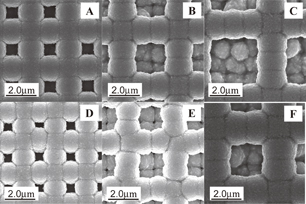
Fig. 4. SEM images of the emitter side of samples A to F.
Download figure:
Standard image High-resolution imageFigure 5 shows the emissivity spectra collected for the emitter sides of samples A, B, C, and D together with a flat Ni–W film. All the measured spectra have absorption peaks at around 4.2 µm, which corresponds to atmospheric CO2 absorption, and plot leaps at 2.5 µm, which are due to focal point alignment error between two instruments. The emissivities of samples A to D are increased at short wavelength ranges from flat Ni–W films. There are two possible mechanisms for this effect: the first one is the artificial increase due to diffraction. The second one is the real increase because of the existence of resonant modes. Since diffraction occurs with the wavelength range of λ < Λ and the condition that the m-th order diffraction is caught by the objective can be expressed as Λ·NA/m < λ, emissivity spectra can be affected especially at the wavelength range of Λ·NA < λ < Λ.

Fig. 5. Emissivity spectra of the emitter side of samples A, B, C, and D.
Download figure:
Standard image High-resolution imageIn Fig. 5, the longest peak wavelengths of samples A, B, C, and D are observed at 1.9, 4.0, 5.7, and 2.5 µm, respectively. Those of B and C are larger than each Λ and agree well with the λ101 estimated on the basis of fabricated dimensions (3.9 and 5.7 µm, respectively). Therefore, as λ101 is larger than λSPP for samples B and C, the governing regime of λC is attributed to single-cavity resonance. In samples A and D, the expected λ101 values from the fabrication result were 1.5 and 1.0 µm, respectively, and they are smaller than the expected λSPP (2.4 µm). The measured longest peak wavelength for sample D agrees well with λSPP. In the case of sample A, the observed peak does not agree with λ101 or λSPP. A possible interpretation of this is the shift of λ101 because of the underestimation of the emitter L value due to the edge extrusion effect during electroplating and the existence of a larger cavity inside. In addition, the spectral overlap between λ101 and λSPP, can also be considered, because a shoulder can be seen around 2.4 µm, while it is very weak and disturbed by a plot leap owing to two instruments. Although the diffraction may affect the peak wavelength ranges of samples A and D, because the diffraction is not the resonant effect and considered to affect broadly as a baseline of spectra, the existence of peak wavelengths can be attributed to resonant modes. The use of an integrating sphere may give a more quantitative result by excluding the contribution of diffraction.
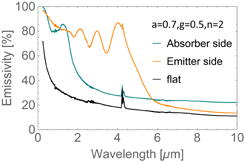
Figure 6 shows the SEM images of the absorber side of samples B, E, and F. The measured L values of 0.6, 0.4, and 0.8 µm, respectively, were slightly different from the designed values (0.82, 0.62, and 1.02 µm, respectively). Figure 7 shows their emissivity spectra. The longest peak wavelengths of samples B, E, and F are 1.3, 1.25, and 1.7 µm, respectively. In samples B and F, the peak wavelengths agree well with the theoretical estimation of λ101 based on fabricated dimensions (1.4 and 1.8 µm, respectively). For Sample E, the result is inconsistent with the estimated λ101 (1.0 µm) or λSPP (1.0 µm). This result can also be due to the incomplete fabrication of a mould or the transfer to a Ni–W film, as shown in Fig. 6, because of the smallest size.

Fig. 6. SEM images of the absorber side of samples B, E, and F.
Download figure:
Standard image High-resolution image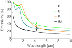
Fig. 7. Emissivity spectra of the absorber side of samples B, E, and F.
Download figure:
Standard image High-resolution imageFigure 8 shows the results of a comparison of the emissivity of the two sides of sample B. Different cutoff wavelengths were achieved on the two sides of the same film. However, the emissivity at the long-wavelength region of the absorber side was increased, which may decrease the conversion efficiency of an STPV because of the re-emission from the absorber. This result is attributed to the film bending as a result of cracks or internal stress on the film.
Fig. 8. Comparison of the emissivity spectra of both sides of sample B.
Download figure:
Standard image High-resolution image
We successfully fabricated films with microstructures on both the front and back sides by an electroplating method and semiconductor processing techniques. Through our mould design, we achieved radiation peaks with different wavelengths. From this point forward, our focus is to test and verify the actual conversion efficiency of the samples in a thermovoltaic system. Moreover, the internal stress of the film must be reduced to increase its strength.
Acknowledgments
The microfabrication in this study is supported by the Nanotechnology Platform program of the Ministry of Education, Culture, Sports, Science and Technology (MEXT) at the VLSI Design and Education Center (VDEC), University of Tokyo. This study is financially supported by the Ring-Ring Project of JKA No. 27-116 and JSPS KAKENHI Grant Number 16K14129.