
Abstract
Sputter-deposited indium–tin oxide (ITO) electrodes became ohmic contacts for unintentionally doped β-Ga2O3(010) substrates with a carrier concentration of 2 × 1017 cm−3 after rapid thermal annealing in a wide range of annealing temperatures of 900–1150 °C. The formation of an ohmic contact is attributed to interdiffusion between ITO and β-Ga2O3, as evidenced by the results of transmission electron microscopy and energy-dispersive X-ray spectroscopy. The interdiffusion decreases the band gap and increases the donor concentration of β-Ga2O3 at the interface, and forms an intermediate semiconductor layer desirable for carrier transport. The ITO ohmic contact is particularly useful for future β-Ga2O3 devices operated at high temperatures.
Export citation and abstract BibTeX RIS
1. Introduction
The formation of ohmic contacts has been one of the major issues for wide-band-gap compound semiconductors, such as SiC, GaN, and ZnSe.1) Compared with narrow-band-gap semiconductors, wide-band-gap ones tend to form Schottky barriers at the metal/semiconductor interfaces because of their large gaps. To decrease the barrier height and/or width, the insertion of an intermediate semiconductor layer (ISL) with a smaller band gap and/or a higher doping concentration has been attempted to improve carrier transport across the interface.2) This ISL formation technology, including electrode material selection and pre- and/or posttreatment, is thus a key to the realization of low-resistivity ohmic contacts, and the technology strongly depends on each semiconductor.3–5)
The fabrication of ohmic contacts for β-Ga2O3 has been attempted along with the accelerated development of β-Ga2O3-based devices. Among compound semiconductors, β-Ga2O3 has recently been widely regarded as a next-generation wide-band-gap semiconductor6–8) owing to its very large band gap of 4.4–4.6 eV9,10) and the availability of large melt-grown single-crystal wafers.11–13) These two attractive features have encouraged the research and development of β-Ga2O3-based devices such as solar-blind photodetectors,14–17) high-power Schottky diodes,18–21) and high-power field-effect transistors.22–25) In these devices, In- and Ti-based electrodes are often utilized as ohmic contacts, where ISLs are formed by pretreatment with plasma exposure,14) reactive ion etching,21–23,25) and ion implantation17,23,25,26) and/or posttreatment of thermal annealing.15,16,19,20,23–25) However, In contact is unsuitable for device patterning because of its low melting point of 157 °C, and Ti contact degrades the electrical properties above 600 °C, probably via the oxidation reaction with β-Ga2O3. Thus, reliable ohmic contacts durable at high temperatures are potentially required to gain a high flexibility of process design and a broad range of device applications.
Here, we propose indium–tin oxide (ITO) ohmic contacts for β-Ga2O3. ITO is widely used as a transparent conductive oxide for optoelectronic applications, and its fabrication processes are already established.27) It is expected that interdiffusion between ITO and β-Ga2O3 upon thermal annealing will result in a desirable ISL for ohmic contacts because ITO is composed of In2O3 and SnO2, which are utilized to decrease the band gap by alloying28) and increase the donor concentration by the substitutional doping of Sn4+ into Ga3+ sites,19) respectively. A similar interdiffusion has already been reported for ITO ohmic contacts to p-GaN, at which a mixed interfacial layer, that is, an ISL, is generated upon rapid thermal annealing (RTA).29) In addition, ITO is considered to have a negligible effect on the series resistance of a β-Ga2O3-based device because the typical resistivity of ITO (10−4 Ω cm) is lower than that of heavily doped β-Ga2O3 (1.4 × 10⁻³ Ω cm).26)
In this paper, we report the successful formation of ITO ohmic contacts to unintentionally doped (UID) β-Ga2O3 substrates by RTA. At the ITO/β-Ga2O3 interface, the presence of the aforementioned ISL layer was revealed by transmission electron microscopy (TEM) and energy-dispersive X-ray spectroscopy (EDS).
2. Experimental methods
The current–voltage (I–V) characteristics of ITO electrodes were compared with those of Ti electrodes as follows. Circular Pt/ITO and Pt/Ti bilayer electrodes (100/140 nm in thickness and 200 µm in diameter for both electrodes) were deposited through a stencil metal mask on chemomechanically polished UID β-Ga2O3(010) substrates with a carrier concentration of 2 × 1017 cm−3 by conventional RF-magnetron sputtering (for ITO) and vacuum electron-beam evaporation (for Pt and Ti) without additional heating. A 2-in. ITO ceramic target ( wt %) was sputtered by Ar ions produced by applying a 100 W RF (13.56 MHz) under an Ar pressure of 8–9 Pa. After the deposition, the samples were annealed in N2 flow under atmospheric pressure for 30 s at various temperatures (800–1200 °C for Pt/ITO and 450–700 °C for Pt/Ti). This RTA process is effective not only to modify the electrode/semiconductor interface structure but also to improve the conductivity of ITO layers. The resistivity of our ITO single layer deposited on an Fe-doped semi-insulating β-Ga2O3(010) substrate under the same deposition conditions was over 106 Ω cm, but the value markedly decreased to 10−4 Ω cm after RTA at higher temperatures of 700–1100 °C, as shown in Fig. 1. To evaluate the electrical properties, I–V measurements were conducted between neighboring electrodes (center-to-center distance was 300 µm) at room temperature. In these measurements, Pt electrodes on ITO contacts were useful in finding where the transparent ITO contacts were. Although the thermal dewetting of Pt was initiated from 900 °C, the dewetted Pt particles on ITO contacts still acted as markers.

Fig. 1. Resistivity of ITO layer on semi-insulating β-Ga2O3 substrate annealed at various temperatures.
Download figure:
Standard image High-resolution imageCross-sectional TEM observation was performed for an ITO/β-Ga2O3 interface after RTA. A TEM specimen was prepared by focused ion beam lift-out and subsequent Ar ion milling for an ITO (140 nm)/β-Ga2O3(010) sample fabricated by sputtering and subsequent RTA at 1000 °C with the same procedures. The interface was observed by bright-field TEM from a viewing direction of [001] under an acceleration voltage of 200 kV. EDS was also performed with an electron probe diameter of 0.3 nm to analyze the composition gradient at the interface. The spatial resolution of EDS was 10–20 nm.
3. Results and discussion
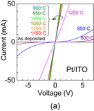
We found a wide process window for forming ITO ohmic contacts. Figures 2(a) and 2(b) show the I–V characteristics of Pt/ITO and Pt/Ti electrodes, respectively. The contact resistances of as-deposited electrodes were so high that the currents between the electrodes were lower than 0.2 and 5 µA at 5 V, for Pt/ITO and Pt/Ti electrodes, respectively. The resistances significantly decreased after RTA, and I–V behaviors changed with the annealing temperature. In the case of Pt/ITO electrodes, I–V curves were nonlinear (double Schottky) at 850 °C and lower temperatures, became linear (ohmic) at higher temperatures of 900–1150 °C, and reverted to nonlinear (double Schottky) at 1200 °C [see Fig. 2(a)]. The reappearance of nonlinearity at 1200 °C may be related to the degradation in the electrical conductivity of the ITO layer, as seen in Fig. 1. This temperature dependence of the I–V characteristics indicates the presence of a wide range of process window, in which the ITO/β-Ga2O3 interface is modified to be desirable for carrier transport. In contrast, we could not find a process window for obtaining Pt/Ti ohmic contacts. Although the electrical properties of the contacts were improved by RTA up to 550 °C, they were degraded at higher annealing temperatures [see Fig. 2(b)]. The failure in forming Ti ohmic contacts may be attributed to a relatively low doping concentration of β-Ga2O3, which is insufficient to decrease the barrier width for carrier tunneling. From these results, the following two important findings are derived. (i) ITO ohmic contacts can be realized for β-Ga2O3 with a relatively low doping concentration (∼1017 cm−3) by postannealing alone. (ii) ITO ohmic contacts maintain their ohmic property even after annealing up to 1150 °C. These advantages over Ti-based electrodes simplify the current device fabrication process and enable the realization of high-temperature operating devices.
Download figure:
Standard image High-resolution image
Fig. 2. Typical I–V characteristics of (a) Pt/ITO and (b) Pt/Ti electrodes annealed at various temperatures.
Download figure:
Standard image High-resolution imageWe confirmed the presence of an ISL layer at the interface by TEM and EDS observations. Figures 3(a) and 3(b) show TEM cross-sectional images near the interface between the ITO layer and the β-Ga2O3 substrate after RTA at 1000 °C. The ITO layer consisted of grains (50–200 nm in diameter) having numerous voids (10–20 nm in diameter, light regions). We speculate that the voids were generated during the high-temperature RTA process because such voids are not seen in conventional ITO layers on glass substrates. The high-temperature annealing also affected the interfacial structure. We can see that the ITO/β-Ga2O3 interface is not abrupt with ambiguous crystal lattices near the interface. In addition, there are some grainlike-structure voids wedging into the β-Ga2O3 side (lighter contrast areas marked by ellipses). This particular interfacial structure suggests that ITO and β-Ga2O3 were interdiffused to create a composition graded layer together with some grains during RTA, and some of the grains on the TEM specimen surface were tipped during the preparation process, leaving grainlike voids.

Fig. 3. (a) and (b) Cross-sectional TEM images at ITO/β-Ga2O3 interface after RTA at 1000 °C. (b) corresponds to the region marked by dashed rectangle B in (a). Ellipses in (a) and (b) indicate voids at the interface (see the text for details). (c) Line profiles of normalized EDS intensities for Ga, In, and Sn at the interface along dashed lines C and C' in (b). The solid and dashed lines of the profiles correspond to lines C and C', respectively.
Download figure:
Standard image High-resolution image
The interdiffusion was also confirmed by EDS line scanning at the interface, as shown in Fig. 3(c). EDS line profiles were taken along lines C (without void) and C' (with void) [see Fig. 3(b)]. Although Ga, In, and Sn intensities for line C' near the interface are lower than those for line C, thus reflecting the void structure, the overall profiles for both lines are similar. Their intensities vary gradually from unity (base material) to noise level near the interface, where the Ga profile and In/Sn profiles are asymmetric. Both Ga profiles have longer tails extending into the ITO side than those of In and Sn into the β-Ga2O3 side. Such asymmetric tailing structures indicate that Ga diffusion into ITO is enhanced compared with In and Sn diffusion into β-Ga2O3, which is reasonable considering the differences in crystallinity between ITO and β-Ga2O3 (low and high qualities, respectively) and ion radius between cations (Ga3+: 0.47 and 0.62 Å, Sn3+: 0.55 and 0.69 Å, and In3+: 0.62 and 0.8 Å for IV and VI coordination numbers, respectively).30) Taking the EDS spatial resolution of 10–20 nm into account, the thickness of the composition graded layer is at least 10–20 nm. We believe that this intermixing layer acts as the aforementioned ISL, and improves carrier transport to realize ohmic contacts.
4. Conclusions
We proposed ITO ohmic contacts for β-Ga2O3 in accordance with the conventional approach of ohmic contact fabrication using the ISL with a small band gap and a high doping concentration. Our prepared ITO contacts indeed had ideal ISL layers and exhibited ohmic behavior after RTA. We are convinced that ITO will be a suitable alternative material for ohmic contacts, particularly for high-temperature stable β-Ga2O3-based devices. To consider practical application, we are now attempting to measure the specific contact resistance of ITO ohmic contacts.
Acknowledgments
The authors would like to thank H. Kawanowa (Ion Technology Center Co., Ltd.) for valuable discussions regarding TEM and EDS analyses. This work was supported by JSPS Grants-in-Aid for Scientific Research (Nos. 26709020 and 16K13673) and a research grant from the JGC-S Scholarship foundation.