

Abstract
High-performance AlGaN/AlGaN hetero-field-effect-transistor (HFET)-type photosensors with high photosensitivity were fabricated using p-type GaN comprising three-dimensional island crystals. The p-type GaN layers were grown on AlGaN layers at a high AlN molar fraction, and the area of p-type GaN comprising three-dimensional island crystals increased as the thickness of the p-type GaN film decreased, resulting in a reduced p-type GaN coverage ratio. The p-type GaN layers comprising three-dimensional island crystals and showing low coverage ratios were then used to fabricate HFET-type photosensors with high photosensitivity. A high light sensitivity of 1.5 × 10⁴ A/W was obtained at a source–drain voltage (VSD) of 0.5 V for a photosensor with a p-type GaN thickness of 20 nm. Moreover, the dark current was suppressed to 10−10 A/mm and the photosensor achieved an extremely high photocurrent to dark current density ratio.
Export citation and abstract BibTeX RIS
1. Introduction
High-performance ultraviolet (UV) light-emitting diodes (LEDs) have been developed for use in sterilization and medical applications.1–10) Accordingly, it is necessary to develop UV photosensors with wavelength selectivity, low dark currents, and a low noise equivalent power.11–14) As AlGaN ternary alloys have wide direct bandgaps ranging from 3.4 to 6.2 eV, they are suitable for photosensors that operate in the near-UV to deep-UV regions.15,16)
Previously, we reported the fabrication of AlGaN/AlGaN heterostructure-field-effect-transistor-type (HFET-type) photosensors with high sensitivity for UV light with wavelengths of 220–280 nm.17) In these photosensors, a two-dimensional electron gas (2DEG) is induced at the undoped Al0.6Ga0.4N/undoped Al0.5Ga0.5N heterojunction interface. A p-type GaN optical gate was also used between the source and the drain. As the 2DEG is not immediately generated at the AlGaN/AlGaN heterointerface beneath the p-type GaN layer, the dark current of photosensors is reduced.18,19) Therefore, this structure realizes both high photosensitivity and low dark current; the photosensors achieve a high photosensitivity exceeding 103 A/W with a dark current on the order of 1 × 10⁻¹¹ A/mm at a source–drain voltage (VSD) of 3 V. In addition, the photocurrent to dark current (Ip/Id) ratio in these photosensors was of the order of 103. Currently, the UV light sensor with the highest photosensitivity is a photomultiplier tube (PMT), which exhibits a photosensitivity of the order of 105 A/W and an Ip/Id ratio of the order of 104 (Hamamatsu Photonics R6354). Thus, to achieve light detection characteristics comparable to those of PMTs, it is essential to reduce the dark current and improve the photosensitivity of the HFET-type photosensor.
Studies conducted on LEDs have revealed that light extraction efficiency can be improved by a surface treatment such as moth-eye processing on the substrate, which increases light intensity.20–30)
Therefore, to increase the photosensitivity of AlGaN/AlGaN HFET sensors, specific surface structures were investigated. It was previously reported that the initial growth of p-type GaN on an AlN layer results in the formation of three-dimensional island crystals, even when p-type GaN is grown on AlGaN using a high AlN molar fraction.31,32) In the present study, p-type GaN comprising these three-dimensional island crystals was demonstrated to improve the photosensitivity of AlGaN/AlGaN HFET-type photosensors. When p-type GaN layers were grown on AlGaN at a high AlN molar fraction, the area of p-type GaN comprising three-dimensional island crystals increased as the thickness of the p-type GaN film decreased, resulting in a reduction in p-type GaN coverage ratio. Specifically, reducing the thickness of the p-type GaN layer from 200 to 20 nm decreased the p-type GaN coverage ratio of the AlGaN barrier layer from 90.3 to 65.3%. HFET-type photosensors fabricated using p-type GaN films with a low coverage ratio and a thickness of 20 nm exhibited a high light sensitivity of 1.5 × 10⁴ A/W at a VSD of 0.5 V. Moreover, the dark current was suppressed to 10−10 A/mm; therefore, the photosensors with the three-dimensional island crystal structure achieved an extremely high Ip/Id ratio.
2. Experimental procedure
Figure 1 shows a schematic view of an AlGaN/AlGaN HFET-type photosensor with a p-type GaN optical gate. Device wafers were grown by metal organic vapor phase epitaxy (MOVPE) on sapphire (0001) c-plane substrates. Trimethylaluminum (TMAl), trimethylgallium (TMGa), bis(ethylcyclopentadienyl)magnesium (Et-Cp2Mg), and ammonia (NH3) were used as the sources of Al, Ga, Mg, and N, respectively. After the growth of a 1.8-µm-thick AlN layer at 1250 °C on the sapphire (0001) c-plane substrate, a 320-nm-thick undoped Al0.5Ga0.5N layer and a 35-nm-thick undoped Al0.6Ga0.4N barrier layer were then grown at 1050 °C. Finally, after flowing Mg for 30 s to form a stable, high-concentration magnesium layer prior to crystal growth, a Mg-doped p-type GaN layer was grown at 1030 °C. The Mg doping concentration of this p-type GaN layer was set at 2 × 1019 cm−3 and determined by secondary ion mass spectrometry analysis. Five samples with different p-type GaN thicknesses of 20, 50, 100, 150, and 200 nm, which were determined by growth rate, were grown. It is difficult to dope Mg at concentrations when the p-type GaN thickness is less than 20 nm; thus, we set the p-type GaN thickness at more than 20 nm. The AlN molar fraction of each AlGaN layer was determined from (0002) 2θ–ω scans and  reciprocal space mapping results obtained by X-ray diffraction analysis.
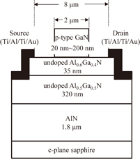
Fig. 1. Schematic view of device structure.
Download figure:
Standard image High-resolution imageTo fabricate each photosensor, the Mg acceptors in the p-type GaN layer were first activated by annealing at 850 °C for 5 min in N2. Mesa isolation was then performed by Cl2 inductively coupled plasma (ICP) etching. A p-type GaN optical gate with a length of 2 µm and a width of 100 µm was also fabricated by ICP etching, except in the photodetection area. The interval between the source and the drain was 8 µm. Subsequently, Ti (30 nm)/Al (100 nm)/Ti (20 nm)/Au (150 nm) layers were deposited as the source and drain on the unintentionally doped Al0.6Ga0.4N barrier layer and annealed at 810 °C in N2. No antireflection coating was applied to any devices in this study.
Photocurrent was measured using a semiconductor parameter analyzer (Agilent Technologies HP-4155B) at room temperature (RT). The monochromatic sensitivity characteristics of the sensors were determined using a xenon lamp (Asahi Spectra HAL-320) and a spectroscope. Current was measured after irradiating the sample with UV light at 10 nm intervals in the wavelength range from 220 to 320 nm. The monochromatic light irradiation density was held constant at approximately 45 µW/cm2.
3. Results and discussion
Figure 2 shows scanning electron microscopy (SEM) images (surface and bird's eye views) of five samples with p-type GaN layers of (a) 200, (b) 150, (c) 100, (d) 50, and (e) 20 nm thicknesses. As shown in Fig. 2, the area of the p-type GaN layer comprising three-dimensional island crystals increased as the film thickness decreased. Table I shows a summary of the p-type GaN coverage ratios in the AlGaN barrier layers. The ratios in each wafer were determined by calculating the exposure ratio of each AlGaN barrier layer from the surface SEM images using image processing software (Asahi-Kasei Engineering Azo v2.5). As shown in Table I, the coverage ratio of the p-type GaN layer correlates with the thickness of p-type GaN and it was greatly reduced at a thickness smaller than 50 nm.
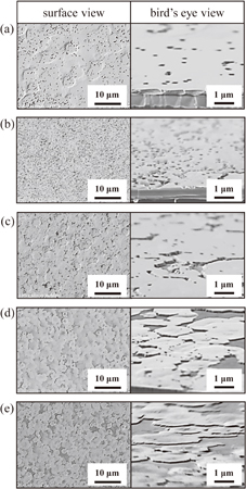
Fig. 2. SEM images (surface and bird's eye views) of five samples with p-type GaN layers of (a) 200, (b) 150, (c) 100, (d) 50, and (e) 20 nm thicknesses.
Download figure:
Standard image High-resolution imageTable I. Coverage ratio of the p-type GaN layer on the AlGaN barrier layer. The values of each wafer were calculated using the exposure ratio of the AlGaN barrier layer as determined from SEM surface images using image processing software (Asahi-Kasei Engineering Azo v2.5).
| p-type GaN thickness (nm) | Coverage ratio of AlGaN barrier layer (%) |
|---|---|
| 200 | 90.3 |
| 150 | 81.5 |
| 100 | 80.6 |
| 50 | 65.8 |
| 20 | 65.3 |
Figure 3 shows the monochromatic photosensitivities of the photosensors fabricated with p-type GaN layers of different thicknesses over the wavelength range from 220 to 320 nm. The peak wavelength for the photosensitivities of the photosensors was 250 nm, and the photosensors did not detect light at wavelengths greater than 300 nm (cut-off). Furthermore, the photosensitivity of the photosensor fabricated using the thinnest (20 nm) p-type GaN optical gate was higher than 104 A/W. Therefore, this photosensor exhibited an extremely high light detection capability comparable to that of PMTs.
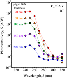
Fig. 3. Monochromatic photosensitivities of photosensors fabricated with p-type GaN layers of different thicknesses.
Download figure:
Standard image High-resolution imageIn addition, the dependences of the photocurrent and dark current on p-type GaN optical gate thickness is shown in Fig. 4. Photocurrent was determined after irradiating each sample at a wavelength of 250 nm (irradiation density: 45 µW/cm2), and dark current was measured at a VSD of 0.5 V. The circles represent the mean of 10 photosensors fabricated with different p-type GaN thicknesses, and the error bars indicate the standard deviation. Notably, the photocurrent increased as the thickness of the p-type GaN layer decreased. The photosensor with a p-type GaN layer thickness of 20 nm exhibited a photocurrent on the order of 10−6 A/mm. Furthermore, although the dark current increased as the thickness of the p-type GaN layer decreased, even in the photosensor with the thinnest p-type GaN layer (20 nm), the dark current was low on the order of 10−10 A/mm. These results confirmed that there is a relationship between the photosensor characteristics and the thickness of the p-type GaN layer.

Fig. 4. Dependence of photocurrent and dark current on the thickness of the p-type GaN optical gate. Photocurrent was determined after irradiation at a wavelength of 250 nm (irradiation density: 45 µW/cm2), and dark current was measured in a dark room at a VSD of 0.5 V. The circles represent the mean of 10 different photosensors fabricated with different p-type GaN thicknesses, and the error bars indicate the standard deviation.
Download figure:
Standard image High-resolution imageNext, we calculated photocurrent to investigate the cause of the current increase, and the calculated values were compared with the experimental values in Fig. 5. The calculations were performed considering only the transmittance of the p-type GaN layer, which was determined using the photocurrents obtained from the photosensor with a 200-nm-thick p-type GaN layer. The transmittance P of p-type GaN is given by

where d is the thickness and α is the light absorption coefficient of the p-type GaN layer. The light absorption coefficient α of p-type GaN at a wavelength of 250 nm was assumed to be 2.0 × 105 cm−1.33,34) As seen in Fig. 5, the experimental values were much higher than the calculated values.

Fig. 5. Comparison of the experimental and calculated photocurrents obtained for photosensors fabricated using p-type GaN films of different thicknesses. The calculated values were determined by considering only the transmittance of the p-type GaN layer based on the photocurrent obtained for a photosensor with a p-type GaN thickness of 200 nm.
Download figure:
Standard image High-resolution imageHere, we discuss the causes of the difference between the experimental and calculated values. Previously, we demonstrated that it is possible to significantly reduce the dark current in the HFET-type photosensors using the p-type GaN gate; in contrast, the dark current of the HFET-type photosensor without the p-type GaN gate is high.14) Therefore, it is important that the depletion layer in this device is formed using the p-type GaN gate.
Therefore, the depletion layer thickness is changed depending on the p-type GaN thickness; thus, we speculated that the 2DEG concentration also changes. We examined the impact of the p-type GaN thickness change on 2DEG concentration by theoretical calculation using band gap modeling software (STR SiLENSe ver5.4). As a result, we confirmed that the 2DEG concentration decreased when the p-type GaN thickness was 5 nm or larger, and that the Mg concentration of p-type GaN was 2 × 1019 cm−3. In addition, the depletion rate did not change with the decrease in p-type GaN thickness (except in the case of 5 nm or less), and the 2DEG concentration was confirmed to be constant. Thus, it is surmised that 2DEG concentration is not affected by the thinning of the p-type GaN.
Alternatively, it is inferred that the electric field applied to the depletion layer increases. Since the resistivity of the depletion layer is high, a large electric field E is applied to the depletion layer. The current density J is given by

where q is the electrical charge, n is the carrier density, and μ is the electron mobility. Because a large electric field is applied when the depletion layer width decreases, the photocurrent increases. So far, we confirmed that current increases in inverse proportion to gate length when the gate length decreases from 3.5 to 1 µm.35) Therefore, it is inferred that the photocurrent in this study increased owing to the short gate effect.
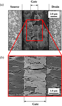
We observed a gate portion to confirm whether a short gate was formed. Figure 6 shows SEM images of the photosensor with a 20-nm-thick p-type GaN layer after device operation [Figs. 6(a) and 6(b) show the surface and bird's eye view images, respectively]. An extremely thin p-type GaN optical gate can be seen in the figure. Therefore, it is considered that the p-type GaN optical gate comprising three-dimensional island crystals created the same effect as a short gate structure. In addition, when the exposed area of the AlGaN barrier layer was increased, the percentage of the short gate also increased. Thus, the short gate effect is thought to be facilitated by the thinning of the p-type GaN layer. Although it is difficult to form extremely short gates of submicron order using conventional photolithography methods, they can be readily manufactured using p-type GaN layers comprising three-dimensional island crystals. In contrast, when the exposed area of the AlGaN barrier layer increased, the depletion of carriers in the 2DEG layer was not sufficient, which is the likely cause of the increase in dark current. However, because the UV light reached the channel layer without being absorbed in the areas of the optical gate where no p-type GaN is present, the photocurrent significantly increased. Therefore, it is concluded that the photocurrent significantly increased owing to the enhancements of the short gate effect and UV light absorption.
Fig. 6. SEM images after using a photosensor with a p-type GaN layer with a film thickness of 20 nm: (a) surface image and (b) bird's eye view.
Download figure:
Standard image High-resolution image
4. Conclusions
AlGaN/AlGaN HFET-type photosensors with very high sensitivity were fabricated using p-type GaN comprising three-dimensional island crystals. The area of the p-type GaN comprising three-dimensional island crystals increased as the film thickness decreased when the p-type GaN layer was grown on AlGaN layers at a high AlN molar fraction. Simultaneously, the coverage ratio of the p-type GaN layer on the AlGaN layer was reduced. Decreasing the thickness of the p-type GaN layer from 200 to 20 nm resulted in a reduction in p-type GaN coverage ratio on the AlGaN barrier layer from 90.3 to 65.3%. An HFET-type photosensor fabricated using a low p-type GaN coverage ratio (20-nm-thick layer) exhibited a high light sensitivity of 1.5 × 10⁴ A/W. In addition, the photocurrent to dark current ratio was greater than 104. Consequently, the performance of this photosensor was comparable to that of a conventional photomultiplier tube.
Acknowledgments
This study was partially supported by the Program for the Strategic Research Foundation at Private Universities, 2012–2016 of the Ministry of Education, Culture, Sports, Science and Technology (MEXT), a MEXT Grant-in-Aid for Specially Promoted Research No. 25000011, and a MEXT Grant-in-Aid for Scientific Research A (No. 15H02019).