

Abstract
Silicon nanowire Schottky barrier tunnel field effect transistors (NW-SBTFETs) are promising structures for high performance devices. In this study, we fabricated NW-SBTFETs to investigate the effect of nanowire structure on the device characteristics. The NW-SBTFETs were operated with a backgate bias, and the experimental results demonstrate that the ON current density is enhanced by narrowing the width of the nanowire. We confirmed using the Fowler–Nordheim plot that the drain current in the ON state mainly comprises the quantum tunneling component through the Schottky barrier. Comparison with a technology computer aided design (TCAD) simulation revealed that the enhancement is attributed to the electric field concentration at the corners of cross-section of the NW. The study findings suggest an effective approach to securing the ON current by Schottky barrier width modulation.
Export citation and abstract BibTeX RIS
1. Introduction
Si-nanowire field effect transistors (Si-NW FETs) are promising device structures for high-performance devices because of their immunity to the short channel effect (SCE) owing to good electrostatic control of the channel.1–8) However, lateral spread of the dopant profile into the channel from the source/drain (S/D) region increases the leakage current in the OFF state,9) and a random dopant fluctuation in the source region causes a variability of NW-FET.10) To solve these problems, a Schottky barrier tunnel FET (SBTFET) with metal S/D, especially silicided S/D, was proposed.11–14) Among various metal S/D, NiSi is one of the most ideal materials owning to low series resistance and low temperature processing for S/D formation.15) In an SBTFET, the gate controls the Schottky barrier tunneling current by modulating the Schottky barrier width (SBW) [Fig. 1]. SBTFETs are known to be immune to SCE as is in the case of NW-FETs.11) Recently, the metal S/D structure has been used to secure the ON current. For example, Zhang et al.16) realized a very steep subthreshold slope of 3.4 mV/dec. Huang et al.17) showed a capability of boosting the ON current of a band-to-band tunnel FET. The ON current is sustained by the tunneling current through the SB between source and channel, so that the enhancement of the tunneling current has a significant impact on the practicality of these devices.

Fig. 1. Schematic view of energy band diagram at source/channel interface in SBTFET.
Download figure:
Standard image High-resolution imageIn this study, we fabricated NW-SBTFETs to investigate the effect of nanowire structure on the device characteristics. We have found that the ON tunneling current is significantly enhanced in narrower NWs.
2. Experimental methods
Figures 2 and 3 show the fabrication process flow of NW-SBTFETs. First, a (100)-oriented silicon-on-insulator (SOI) wafer was thermally oxidized in dry O2 atmosphere at 850°C for 3 h to form a thermal SiO2 film on the SOI surface [Fig. 3(a)]. The SOI layer is a p-type Si with a dopant density of 1.0 × 1015 cm−3 and is 45 nm thick. The thickness of the buried oxide (BOX) layer is 145 nm, and the total thickness of the SOI wafer is 750 µm. The thermal SiO2 film was used as a hard mask for the following patterning process of NWs and contact pads.
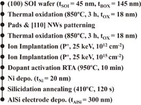
Fig. 2. Process flow of NW-SBTFET fabrication.
Download figure:
Standard image High-resolution image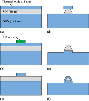
Fig. 3. Schematic of oxidized Si-NW fabrication.
Download figure:
Standard image High-resolution imageThe SiO2 hard mask was patterned by electron beam lithography and etching with a buffered hydrofluoric acid (BHF) solution [Figs. 3(b) and 3(c)]. Next, the SOI layer was etched with tetramethylammonium hydrooxide solution18,19) to fabricate the NWs with 〈110〉 orientation and contact pads [Fig. 3(d)]. The sidewalls of NWs are oriented with the {111} plane. Both ends of the bundle of 10 NWs are connected to a pair of contact pads.
After the patterning, the SiO2 hard mask was removed by BHF, followed by thermal oxidation in dry O2 atmosphere at 850 °C for 3 h to form a thin oxide layer to protect the NW surface. The thermal oxide thickness is 18 nm. The Si-NW core width (W) varies from 68 to 120 nm. After oxidation, phosphorous ions (P+) were implanted with an energy of 25 keV with a dose of 1.0 × 1012 cm−2. To form ohmic contacts on the drain-side pad, P+ ions were implanted with a dose of 1.0 × 1015 cm−2 at a beam energy of 25 keV, followed by activation annealing at 950 °C for 10 min.
Next we removed a part of the oxide layer covering NWs and the source-side pads by BHF, and 20 nm thick Ni was deposited by sputtering. Then, Ni silicide was formed by annealing at 410 °C for 120 s. The unreacted residual Ni was removed by a mixture of sulfuric acid and hydrogen peroxide. The oxide layer on the drain-side pad was removed by BHF, and 300 nm thick AlSi was deposited by sputtering. Finally, AlSi electrodes were patterned by etching in a mixture of phosphoric acid, acetic acid, and nitric acid.
A schematic of the fabricated device is shown in Fig. 4(a). Figures 4(b) and 4(c) show a scanning electron microscopy (SEM) image of Ni silicide NW and a cross-sectional SEM image of Si-NWs, respectively. The NW length is 5 µm. In Fig. 4(b), the Ni silicide region is observed as relatively bright colors in the left part of the image.20) FET operation was performed by applying a backgate voltage (Vbg). The electrical properties were observed by an Agilent B1500A semiconductor device analyzer.

Fig. 4. (a) Schematic of SBTFET, (b) SEM image of Ni silicided NW, and (c) SEM image of cross-sectional NW. The NW width ranges from 68 to 120 nm.
Download figure:
Standard image High-resolution image3. Results and discussion
To confirm silicide/Si Schottky contact formation, we evaluated the diode characteristics by measuring the Jd–Vds relationship at Vbg = 0 V [Fig. 5(a)]. The forward bias current was linearly extrapolated to zero volt to obtain the thermionic emission current JS [inset of Fig. 5(a)] in the Richardson–Dushman equation21) given by

where A* is the effective Richardson constant of Si with a value of 110 A cm−2 K−2, T is the temperature, q is the elementary charge, ΦB is the Schottky barrier height (SBH), V is the applied voltage, and k is the Boltzmann's constant.
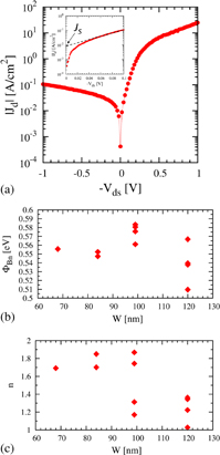
Fig. 5. (a) Diode characteristics of SBTFET for NW width of 120 nm, (b) correlation between Schottky barrier height ΦB and NW width W, and (c) correlation between ideal factor n and NW width W.
Download figure:
Standard image High-resolution imageThe SBH estimated by the thermionic emission model ranges from 0.50 to 0.60 eV [Fig. 5(b)], which is lower than the value of 0.67 eV found in the literature22) for a planar NiSi/Si interface. The ideal factor n estimated by the thermionic emission model increases as the NW narrows [Fig. 5(c)], indicating that the electron–hole recombination rate is greater in narrower NWs.
In NWs with 120 nm width, Id increases exponentially with Vbg [Fig. 6(a)]. A comparison of the Id–Vbg characteristics of 68 and 120 nm wide NWs at Vds = 0.5 V [Fig. 6(b)] shows that the ON current density is enhanced in the narrower NW devices. At Vbg = −10 V, OFF leakage current is observed for the 68 nm wide NW, which contrasts the characteristic exhibited by the 120 nm wide NW. The OFF leakage current can be attributed to the electron–hole recombination current, which is supported by the degradation of the ideal factor in narrower NWs [Fig. 5(c)].
Download figure:
Standard image High-resolution image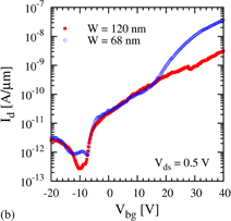
Fig. 6. Id–Vbg characteristics (a) for various drain voltages Vds and (b) with different NW widths.
Download figure:
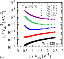
Standard image High-resolution imageThe Fowler–Nordheim (FN) plot23,24) shows a negative linear slope for Vbg > 20 V [Fig. 7(a)]. This region with the negative slope does not depend on the temperature [Fig. 7(b)], meaning that the dominant current component is the FN tunneling through the SB, and not the thermionic emission. In low Vds region (1/Vds > 3), the FN plot depends on the temperature, which indicates that thermionic emission current becomes dominant. Therefore, our fabricated NW devices can be confirmed as operating as an SBTFET in the high Vds region.
Download figure:
Standard image High-resolution image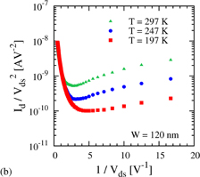
Fig. 7. FN plot for (a) various backgate voltages Vbg and (b) various temperatures for Vbg = 40 V.
Download figure:
Standard image High-resolution imageThere may be two sources for the enhancement of the ON current density in narrower NW devices: (1) the increase in the tunneling current by trap-assisted tunneling (TAT) and (2) SBW modulation due to the electric field concentration at the NW edge. The basis for the hypothesis (1) is provided by the present experimental results. As shown in Fig. 5(c), the ideal factor is degraded in narrower NWs, which indicates an increase in the trap density in the SB. The origin of the trap is considered as the surface defects of Si-NWs in the vicinity of the silicide/Si interface. The narrower NWs have larger specific surface area, so that the effect of the surface trap is more significant. Therefore, TAT via these traps may contribute to the enhancement of the ON current. In this regard, Mori et al. proposed an ON current boost technology of the band-to-band tunnel FET by intentionally generating isoelectronic traps (IETs).25–27) The second hypothesis is based on the peculiar shape of our fabricated NW devices. As shown in Fig. 4(c), the cross-sections of the fabricated NWs are trapezoidal in which the bottom edges have an acute angle. Therefore, the electric field may concentrate at the bottom edges of NWs when a backgate voltage is applied. In what follows, we discuss the possibility of these hypotheses.
To estimate the contribution of TAT, we carried out a two-dimensional TCAD simulation.28) Universal Schottky tunneling model29,30) and Schenk model31) were employed to reproduce the Schottky barrier tunneling (SBT) and TAT, respectively (Fig. 8). Figure 9 shows a schematic of the simulated device structure, and Table I lists the parameters. The contact resistance was set to 2500 Ω on the basis of the measured contact resistance value of a test element group (TEG) on the same wafer. The SBH at the channel (n+-Si)/drain interface was set to 0 eV.
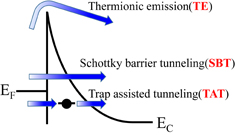
Fig. 8. Schematic of current component through Schottky barrier.
Download figure:
Standard image High-resolution image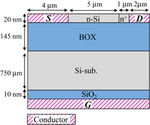
Fig. 9. Schematic of simulated device structure.
Download figure:
Standard image High-resolution imageTable I. Device parameters used in simulation.
| Drain voltage (V) | 2.0 |
| Work function (eV) | 4.7 |
| Doping density (n) (cm−3) | 1.0 × 10¹⁶ |
| Doping density (n+) (cm−3) | 6.5 × 10²⁰ |
| Trap density (cm−3) | 4.0 × 10¹⁷ |
| Trap level (eV) | 0.9 |
| Contact resistance (Ω) | 2500 |
The Id–Vbg characteristics of the simulated device reproduce the experimental result of the 90 nm wide NW (Fig. 10) because TAT induces OFF-state leakage current and degrades the subthreshold slope. However, TAT does not contribute to the ON current density, which differs from the case of band-to-band tunnel FETs using IET-assisted tunneling.25–27) The difference in the impact of TAT between the SB tunnel and the band-to-band tunnel can be understood as follows. SB tunneling preferentially occurs at the Fermi level, because the barrier width increases as the energy level decreases. Therefore, even if the channel includes a high density of intra-band traps, the effect of TAT hardly depends on the gate bias. On the other hand, band-to-band tunneling uniformly occurs between the valence band top of the source and conduction band bottom of the channel. Therefore, the TAT current enhances the ON current in band-to-band tunnel FETs.
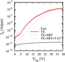
Fig. 10. Experimental and simulated Id–Vbg characteristics.
Download figure:
Standard image High-resolution imageWe investigated the possibility of the second hypothesis by analyzing the electric field distribution in the 60 nm wide NW [Fig. 11(a)] and 120 nm wide NW [Fig. 11(b)] at Vbg = 40 V. The electric field is concentrated at the bottom edges of the NW, and the extent is larger in the narrower NWs. The enhancement of the electric field in the narrower NW is induced by the interference between the fringe fields around the bottom edges of the NW. The ON current flows are concentrated in the high electric field part of the NW, which leads to the increase in the current density in the narrower NW. This is numerically demonstrated by the three-dimensional TCAD simulation [Fig. 12]. The simulated Id–Vbg characteristics clearly show that the ON current density enhancement can be attributed to the electric field concentration in narrow NWs.
Download figure:
Standard image High-resolution image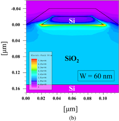
Fig. 11. Simulated electric field distribution for Vbg = 40 V with NW width of (a) 60 and (b) 120 nm.
Download figure:
Standard image High-resolution image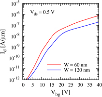
Fig. 12. Simulated Id–Vbg characteristics for NWs with 60 and 120 nm width. The simulation takes thermionic emission current and SBT current into account, and employs the same device structures shown in Fig. 11.
Download figure:
Standard image High-resolution image
It has been reported that a rectangular Ω-gate NW-MOSFET exhibits high drivability due to high inversion electron density concentrated at the corners of NW8,32) as well as the present analysis. Therefore, a cross-sectional shape including corners at sharp edges is more preferable than a circular shape for enhancing the ON current of NW devices of both conventional MOSFETs and SBTFETs.
4. Conclusions
NW-SBTFETs with different NW width were fabricated, and we found that the ON current density is enhanced in narrower NWs. The ON current density enhancement is explained by the SBW modulation due to concentration of the electric field at the bottom edges of NWs. To secure the ON current density by SBW modulation, engineering the NW shape with corners is an effective approach.
Acknowledgments
This work was supported by a Grant-in-Aid for Challenging Exploratory Research (26630135) from the Ministry of Education, Culture, Sports, Science and Technology, Japan. We are grateful to Professor T. Tanii for advice on electron beam lithography process, Mr. O. Hirai of Waseda University Micro Technology Lab. for assistance with the ion implantation process, and Mr. T. Sasaki of Waseda University Research Organization for Nano and Life Innovation for advice on electrical characteristics measurement.