
Abstract
This paper presents a review on state-of-the-art of thin-film transistor (TFT) technology and its wide range of applications, not only in liquid crystal displays (TFT-LCDs), but also in sensing devices. The history of the evolution of the technology is first given. Then the standard applications of TFT-LCDs, and X-ray detectors, followed by state-of-the-art applications in the field of chemical and biochemical sensing are presented. TFT technology allows the fabrication of dense arrays of independent and transparent microelectrodes on large glass substrates. The potential of these devices as electrical substrates for biological cell applications is then described. The possibility of using TFT array substrates as new tools for electrical experiments on biological cells has been investigated for the first time by our group. Dielectrophoresis experiments and impedance measurements on yeast cells are presented here. Their promising results open the door towards new applications of TFT technology.
Export citation and abstract BibTeX RIS
1. Introduction
Thin-film-transistor (TFT) technology is a well-known technology widely used in flat-panel displays, computers, smart phones, video game systems and personal digital assistants. This technology has revolutionized video systems, allowing flat panels with increasingly larger dimensions to be obtained: 164 in. is the diagonal dimension of the substrates used nowadays for TFT liquid crystal display (TFT-LCD) fabrication.
TFTs are actually MOSFET transistors. Their fabrication technology has a history almost as long as that of CMOS technology, but it took several decades before it was mature enough to reach the production level.1) Actually the improvement and development of TFT technology has three aspects: the improvement of the semiconductor layer, the stability of the process for large scale fabrication, and the development of process equipment to produce increasingly large devices. Initially it was mainly the first aspect that limited the rate of the development of this technology. In Sect. 2, we present the history of the development of TFT technology.
This technology was applied from the beginning to TFT-LCDs. However, other applications have been investigated in the last 20 years, in areas as diverse as X-ray detection,2,3) microelectronic devices (memory4)), chemical sensing,5,6) and bio-chemical sensing.7) In the last field, organic thin film transistors (OTFTs) have played an important role.8) These applications and their working principles are described in Sect. 3.
TFT technology has, however, to our knowledge, never been used for biological cells applications. We believe that the structure of TFT array substrates fabricated by this technology might make them extremely useful as electroactive substrates for electrical manipulation as well for electrical sensing on biological cells. We also believe that such substrates might have a wider range of applications than multi electrode arrays (MEAs) realized by more standard microfabrication techniques or by CMOS processing.9–11) Finally, we intend to develop and use such devices as electronic platforms for extended in vitro electrical studies on biological cells.
Section 4 thus explains for which aspects TFTs might be of interest for electrical in vitro experiments on biological cells, by comparing them with more standard devices with microelectrodes such as MEAs and CMOS.
We have performed several types of experiments on TFT array substrates, which might be applied to biological cells. Our goals are twofold. First, we would like to investigate the areas of use of TFT array substrates and their limits. At the same time, we would like to develop a TFT platform for biomedical applications, and to study in vitro particular diseases, by performing electrical and optical analyses. In particular, we aim to study in vitro amyotrophic lateral sclerosis (ALS), a disease which results in the death of neurons that control muscle cells.12) Towards achieving this aim, we are investigating several possible areas of application for such a platform. Experiments on the use of dielectrophoresis (DEP) to place, separate, and release cells, and on the use of impedance spectroscopy to monitor the growth and viability of cells have been performed and are presented Sect. 5. The experiments were performed with yeast cells as they are easier to manipulate and to culture than neurons and muscle cells.
Finally, we discuss the positive aspects of these first results and the known limits of TFT array substrates as electroactive platforms, in Sect. 6.
2. History of development of TFT technology
The first TFT was fabricated in 1962, about two years after the fabrication of the first MOSFET, and TFTs are actually MOSFET transistors.13) In 1973, the first TFT-LCD was demonstrated,14) defining the main direction of the research and development for TFT technology.
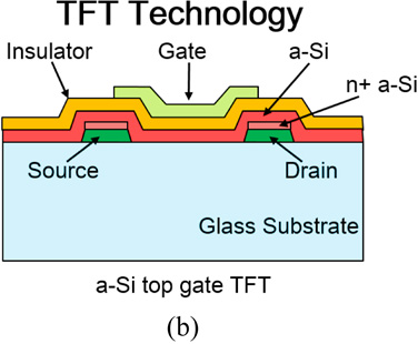
TFTs and MOSFETs do not face the same problem in their fabrication. This difference explains why it took more than two decades for TFT-LCDs to reach commercialization. The main difference between CMOS technology and TFT technology resides in the process steps. CMOS technology involves, among other step: implantation, layered growth from the substrate, and deposition, while TFT technology only involves deposition. This has important consequences, for the crystalline quality of the source and drain pockets and the channel: the carrier mobility is clearly much higher in CMOS than sin TFTs because of the preservation of the crystallinity with the implantation technique, while deposition allows only amorphous layers to be obtained. On the other hand, a major advantage of TFT technology over CMOS technology is that, since only a deposition process is involved, transistors can be fabricated on any kind of substrate, including glass and plastic which are transparent with almost no limitation on the size of the substrate. This explains why the technology has since the beginning been preferred for the development of LCD panels. Figure 1 shows typical cross-sections of a p-MOSFET and a top gate n-type TFT with amorphous silicon as the semiconductor material for the channel. Table I lists the differences in the fabrication technologies.

Download figure:
Standard image High-resolution image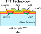
Fig. 1. Cross section of (a) p-MOSFET and (b) amorphous silicon top-gate TFT. TFT technology uses only deposition for the growth of the layers, while CMOS technology uses also implantation and growth from the substrate.
Download figure:
Standard image High-resolution imageTable I. Comparison of CMOS technology and TFT technology.
| CMOS technology | TFT technology | |
|---|---|---|
| Layer growth technology | Implantation, deposition, growth from substrate | Deposition (sputtering, PECVD) |
| Process temperature | High temperature (> 600 °C) | Low temperature (< 600 °C) |
| Quality of layers | High crystalline quality of source and drain pockets and channel | Amorphous or polycrystalline |
| Carrier mobility in the channel (cm2 V−1 s−1) | 500 | 0.5–200 |
| Type of substrate | Semiconductor substrates: opaque | Any kind of substrate, including glass or plastic: transparent |
| Substrate dimensions | Millimeter size | Centimeter to meter size |
The first TFT was a CdS TFT, which was followed by a CdSe TFT in 1973.13,14) Both had a reasonably high carrier mobility, of above 40 cm2 V−1 s−1. However, owing to difficulties in the fabrication, such as the stability of the quality of the semiconductor on a large surface, and the reliability of the devices, application to LCDs did not reach commercialization. At the beginning of the 1980s owing to the development of hydrogenated amorphous silicon (a-Si:H), which greatly improved the stability and the characteristics of TFTs, this technology underwent a major improvement, allowing the production of active matrix (AM) LCDs, and: in 1989 the first TFT-LCD was commercialized. Improvement of the semiconducting layer followed owing to with the development of other materials. Table II summarizes the evolution and compares the different semiconductor materials developed for TFT-LCDs, since the 1960s. The development of transparent oxide semiconductors such as indium gallium zinc oxide (IGZO) was a major step forward in improving even further characteristics of TFTs. Power consumption was further reduced due to the high carrier mobility, and transparent transistors were obtained giving larger aperture ratio of the LCDs.15)
Table II. Evolution and description of the semiconductor materials used in TFTs.
| Compound semiconductor | Year of development | Deposition technology | Carrier mobility (cm2 V−1 s−1) | Description |
|---|---|---|---|---|
| CdSe | 1971 | PECVD | 40 | High mobility but difficulty in large-scale processing |
| a-Si:H | 1979 | PECVDb) | 1 | Suitable for large-scale processing |
| poly-Si | 1996 | a-Si:H depo. + laser annealingc) | 100 | High mobility |
| Organica) | 2000 | Evaporation, coating | 0.1–30 | Transparent Easy and cheap fabrication Many semiconductor polymers |
| IGZO | 2004 | Sputtering | 10–20 | Transparent material High mobility |
a) pentacene, rubrene, PPV, etc.
b) from SiH4
c) over 1000 °C
The dimensions of products are another aspect of the development of the technology. The first commercialized TFT-LCD had a diagonal dimension of 10.4 in. Nowadays, TFT-LCD manufacturing plants are involved with the 10th generation of the mother glass, which corresponds to glass substrates as large as 2850 mm per 3050 mm (164 in.). The 11th generation of the mother glass, 3200 mm per 3600 mm (189 in.) is under development and should be implemented soon. Behind the fabrication of increasingly large panels, companies, such as SHARP, LG, Samsung, and Innolux are making considerable effort to develop stable processes on large-scale substrates and to create increasingly large equipment for the deposition, lithography, etching, and testing of even larger substrates.
The main application of TFTs is LCD panels. However, TFTs are also widely used in X-ray detectors as sensors. TFT devices can also be found in many sensing applications. State-of-the-art applications using TFT technology are reported in the following section.
3. State-of-the-art applications using TFT technology
With the development of TFT technology for TFT-LCDs, new applications began to appear from the 90's. At the end of the 90's flat-panel X-ray detectors were commercialized3) for medical diagnoses such as the detection of fractures, lesions, and tumors. In these systems, the detection of X-rays can be performed using photodiodes fabricated on top of the TFTs.3) Another more common way is to cover the surface of the TFT array substrate with a layer of an X-ray photoconductor material such as cadmium telluride (CdTe). When an incident X-ray reaches the surface of the photoconductor, an electric charge corresponding to the incident X-ray dose is produced that migrates towards the pixel electrode then is stored in a storage capacitor integrated inside the TFT array.16) A greatly enhanced resolution can be achieved with such devices, which are widely produced by companies including Fujifilm.
Some physical sensors, such as resistive pressure sensors, are among the most widely used and have been developed for TFT touch screens. They have been manufactured since the beginning of the 2010's by companies including LG Display, AUO, and JDI.17) The TFT array substrate is integrated with an OLED layer and a pressure sensor layer. The latter transduces a pressure into an electrical signal, which is in turn transmitted to TFTs which control and modulate the OLED. The pressure sensor can be a pressure sensitive rubber whose resistance changes with the pressure, such as poly(methyl methacrylate) (PMMA) or a soft polymer containing conductive particles.18)
Other physical sensors applications for e-skin technology for instance, when TFTs are fabricated on a flexible substrate, using organic-TFTs (OTFT), have great interest for robotics.19) Finally, uncooled infrared sensors arrays for thermal imaging are other types of physical sensors for applications like IR spectroscopy, pollution control or monitoring of semiconductors wafers during processing.20,21)
In parallel to physical sensors, many studies have been performed in the field of chemical and biochemical sensing.
For all these sensors, postprocessing of the TFT array substrate is needed in order to add a layer sensitive to the species to be detected. Many of these sensors are OTFTs because of the easier postprocessing. Among the chemical sensors, ion-sensitive field-effect transistor (ISFET) sensors are well known. In such devices the gate of the TFT has to be extended in order to increase the area of the surface used for detection, and these sensors have to be covered with a thin layer of an insulator such as silicon nitride. A typical sensitivity of 54 mV/pH has been reported.22)
Concerning TFT gas sensors, many applications related to the environment and the detection of hazards have been realized. They are in competition with commercially available gas sensors, which are often based on metal oxides and operate at high temperatures. The advantages of TFT gas sensors are the short response time, high sensitivity, and room-temperature functioning. However, stability with time and usage is a limitation. They use conductive polymers as active layers, which are easy to fabricate by deposition and whose structure and composition can be adjusted according to the application and the species to be analyzed.23) The active layer is a transducer, which converts chemical information (concentration, compound) into a physical signal by means of chemical reactions or the absorption of molecules. Chemical reactions and absorption change the electrical characteristics of the polymer layer, causing a change in the source–drain current or in the gate voltage. These sensors have been developed for various applications, such as single-chemical (ammonia, toluene, propanol, and humidity sensing), as well as for the discrimination of a mixture as an electronic nose.6,8,24)
Most TFT biosensors are based on OTFT technology. Those that are not based on OTFTs generally use semiconductors with high mobility such as ZnO or carbon nanotubes. Many applications involve the fabrication of immunosensors for cancer detection.25,26) Biosensors are very specific sensors, as molecular recognition is usually performed by means of complementary couples such as antigens/antibodies, and enzyme/enzymatic substrate or by the hybridization of a DNA-probe strand and a DNA-target strand. Similarly to chemical sensors, a sensitive layer is necessary to transduce the biochemical signal into a physical parameter that is electrically measurable. The antibodies, enzyme, or DNA-probes are attached onto the sensitive layer. The reaction of the target molecules with the complementary molecules changes the surface electrical characteristics of the sensing layer, causing charge accumulation or increasing or decreasing the conductivity. These variations are detected by the TFT whose source–drain current is modulated by these effects. The first applications that were targeted were the detection by enzymatic reactions. In particular, glucose sensing using glucose oxidase was among the first targets.27,28) Other enzymatic OTFT sensors were developed afterward for the sensing of urea, penicillin and lactates.29–31) Non-enzymatic OTFT sensors have also been reported for the sensing of: lactic acid, biotin, C-reactive protein (CRP), which is an important protein for detecting cardiovascular diseases, and DNA.26,32,33)
TFT technology has been used not only for LCDs, but also for physical, chemical and biochemical sensing. However, the structure of the TFT devices used for LCDs exhibit very interesting characteristics for applications involving biological cells and can potentially be used as an electrical platform for experiments on cells.
The following section begins with a description of the features of TFT devices. Then the basis of their features on possible biological cell applications are discussed.
4. Possible use of TFT devices for cell-based applications
4.1. Description of TFT array substrates and features
The TFT array substrates discussed in this article were directly taken from the screens of smart phones.
Figure 2(a) presents a close-up view of a screen observed with a microscope. The RGB (red, green, and blue) pixels are clearly seen. Figure 2(b) shows the cross section of a screen. This screen consists of a lower glass, called a "TFT array substrate" in this review article, with a polarizer on the bottom and an array of TFT pixels on the top, and an upper glass with a color filter on the bottom and another polarizer on the top. Between both glasses, a spacer filled with liquid crystal can be found.
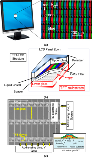
Fig. 2. Description of a TFT-LCD panel. (a) Microscopic view of a screen; the RGB pixels can be clearly seen. (b) Schematic cross section of a TFT-LCD panel; the lower glass is called "TFT array substrate". (c) Microscopic view of the lower glass with the array of ITO microelectrodes connected to the drain of the corresponding TFT.
Download figure:
Standard image High-resolution imageThe working principle is as follows. Light coming from the inside of the screen and arriving at the bottom of the TFT array substrate crosses the whole device. If one TFT pixel is switched on, the liquid crystal changes its conformation in the pixel area, and the light can no longer cross the upper glass in this pixel area. In this way, RGB colors can be selected.
Figure 2(c) is a microscopic view of a lower glass with a cross section of a p-Si bottom-gate TFT. The array of TFT pixels is an array of indium tin oxide (ITO) microelectrodes connected to the drain of an array of TFTs. The TFTs on one line have a common source line, while the TFTs on one column have a common gate line. When applying a voltage to one gate line and one source line, the TFT at the intersection of both lines is switched on. All other TFTs are still off. The ITO electrode connected to the drain of the TFT that is on also becomes polarized. In this way, it is possible to individually control each ITO electrode.
The substrate of the TFT is glass, which is transparent. ITO is also transparent, which means that ITO microelectrodes are transparent. TFT array substrates are thus transparent glass substrates with a dense array of transparent microelectrodes. The only nontransparent parts are the source and gate lines and part of the transistors, if they are made of IGZO.
Typical microelectrodes have dimensions of 30 × 100 µm2 and are separated by 5 µm. Thus, around 82% of the surface is occupied by microelectrodes.
Since transistors have a width and length of between 5 and 10 µm and gate and source lines have a width of around 5 µm, about 80% of the surface is transparent.
4.2. Possible use of TFT array substrates for experiments on biological cells
When working with biological cells in in vitro studies, optical observation of the shape, organization, motion, and structure of cells under white or fluorescent light is essential to study phenomena. Standard optical analyses use inverted microscopy, which allows close-up view observation, from the bottom and through the substrate, of the cells cultured on the substrate. Inverted microscopy observation allows more precise observation than conventional microscopy, in the case that cells are cultured in a Petri dish or in microchambers. However, this type of observation is limited to transparent substrates.
Optical observation with a microscope is a key technology used for decades which has proven to obtain accurate analyses. However, in addition to optical analyses, electrical experiments are of great interest and can be complementary to optical analyses. In particular, using microelectrodes, numerous electrical experiments can be performed very locally on biological cells inside a cell culture.34)
Toward realizing an in vivo environment with an in vitro system, it is essential to work with cell cultures and, if possible, with multiple cultures of cells, as this is the case in the human body. However, at the same time, the analysis of a few cells or single cells out of many cells, such as single neuron excitation or activity recording, or following up the growth or viability of a cell culture, becomes more complex. By integrating microelectrodes on a substrate, another type of data can be obtained, which might confirm and complement optical data, and new types of experiments can be performed at the same time. In particular, electrical measurements do not require a fluorescent dye for detection, while, for instance, the optical observation of neuron excitation requires fluorescence. Also, quantitative data can be directly obtained by a simple potential measurement. For instance, the rate of growth of a cell culture or the deterioration of the viability of cells under certain experimental conditions can be more precisely monitored and instantaneously measured by impedance spectroscopy with microelectrodes than by simple optical observation.35) Finally, by integrating microelectrodes on a substrate, electrical experiments on a single cell or a few cells out of many cells can be performed such as the electrical excitation or the activity potential measurement of a single neuron cell;11) the DEP of cells to gather, release, and separate them;36) and the impedance measurements to monitor cell adhesion or growth,37) cell viability,38) and cell differentiation.39)
The above discussion demonstrates the advantages of integrating microelectrodes on substrates for advanced investigations of cell cultures.
In terms of devices, substrates with integrated electronics, which already exist for experiments on cells, can be either MEA devices, such as those commercially available through MED64 Company, or CMOS devices with an integrated array of microelectrodes or sensors.10,11) However, for both technologies, the area with the microelectrodes remains small (mm2), which is a limitation if a multicellular culture is studied for instance. Moreover, the density of microelectrodes in MEAs is as low as 20%, often causing misalignment problems between the cells and the microelectrodes. Also, CMOS devices are not transparent, which limits the precision of optical observation.
Comparing TFT array substrates with the above devices, they can be considered as advanced MEAs. Actually, such substrates can be envisaged as large transparent electroactive substrates. Their transparency allows observation with an inverted microscope. The area with electrodes is much larger than that MEAs and CMOSs, as substrates can be cm2 size or even larger if needed. They can be as large as standard Petri dish boxes or 96-well plates, which are widely used in cell biology. Such dimensions, allow us to investigate multicell cultures, or to create large multipurpose microfluidic devices. The high density of individually addressable microelectrodes provides the possibility of activating individual electrodes at the desired location on the device, without taking into consideration the alignment between the electrodes and cultured cells. This problem of alignment is a current one in the case of MEAs fabricated with standard microtechnology.
On the basis of these considerations, we have investigated the possibility of using TFT array substrates as electrical platforms for biological cell applications, also allowing optical observation. We focused on using the TFTs as switches to control and apply DC or AC signals to ITO microelectrodes. We performed a set of experiments to determine the area of utilization of such substrates. Electrical characterization in DC and AC of the device, as well DEP and impedance measurements were then performed for this purpose and are presented in the following section.
5. Electrical experiments on TFT array substrates
5.1. TFT array substrates and the experimental setup
The TFT array substrates used in our research were obtained by detaching the upper glass of a TFT-LCD for a smart phone from the lower glass. The lower glass was used as a substrate as it contains an array of microelectrodes controlled by individual TFTs, similar to the one in Fig. 2(c). The TFT array substrate was then cleaned, with acetone then ethanol and rinsed with deionized water (DIW) to remove the liquid crystal material.
Once cleaned, the substrate was wire-bonded to a printed circuit board. A microfluidic chamber or a microfluidic channel made of PDMS was attached onto the substrate to contain the liquid during experiments. The gate lines were connected to a power supply, and the source lines were connected to a function generator. The whole system was placed under a microscope for observation during the experiments. Figure 3 presents the setup used. The first experiment performed was to characterize the TFTs.
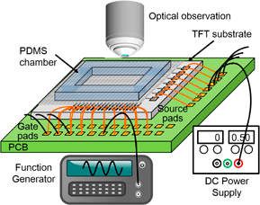
Fig. 3. Setup used during the experiments.
Download figure:
Standard image High-resolution image5.2. Electrical characterization of one TFT
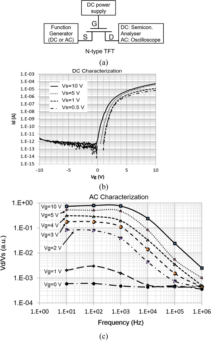
TFTs used for screens are n-type transistors operating under DC voltage. However, many electrical experiments on biological cells require AC voltage, such as DEP and impedance spectroscopy sensing. This is the reason why DC and AC characterizations of one TFT were performed, the results of which are presented in Fig. 4. Figure 4(a) shows the equivalent circuit of one TFT as connected for the measurements. A DC voltage was applied to the drain by a DC power supply, a DC or AC voltage was applied to the source by a function generator, and the output signal from the drain was measured by placing a probe on one ITO electrode with an Agilent B1500A semiconductor analyzer in the case of DC characterization and with an oscilloscope in the case of AC characterization. For AC characterization, as shown in Fig. 4(c), clear attenuation of the output signal at the microelectrode with increasing frequency is observed for frequencies above 1 kHz. This is due to the characteristics of the TFTs. This means that when working with higher frequencies, the amplitude of the output signal will be lower.

Fig. 4. Characterization of one TFT. (a) Equivalent circuit of a TFT as connected for the measurements. (b) DC characterization: graph Id(Vg) for source voltages of 0.5, 1, 5, and 10 V. (c) AC characterization of the drain voltage versus the frequency. Attenuation of the signal can be observed at frequencies above 1 kHz.
Download figure:
Standard image High-resolution image5.3. Bio-compatibility and microfluidic compatibility of TFT array substrates
Before beginning electrical experiments on cells, experiments on the biocompatibility of the substrates were conducted to demonstrate the good biocompatibility with fibroblast cells, primary brain neurons from chicks and liver cells. The adhesion of these cells on the substrate has to be improved however. Part of these results have been published in Ref. 40. The possibility of attaching a microfluidic device made of PDMS on top of the surface as well as observation through the substrate with a fluorescent inverted microscope was also confirmed.40)
5.4. Electrical manipulation by dielectrophoresis with TFT array substrates
DEP is a technique to catch, repulse, and separate cells.36) The principle consists of applying an electric field gradient to induce a dipolar moment on a cell or particle, which in turn is displaced either towards the maximum of the field gradient (positive DEP) or towards the minimum of the field gradient (negative DEP) according to the permittivity of the particle, that of the medium, and the frequency of the AC signal applied. This technique is often used for the separation of particles or cells. The signal has frequencies from kHz to MHz order and amplitudes from 100 mV to V order.
The structure of TFT array substrates is ideal for performing DEP locally, in particular, to place cells in particular areas on the device or to release them on selected areas. It can be used for patterning cells, concentrating cells, and recovering cells after experiments. DEP has been performed on microbeads and yeast cells in DIW, which has a resistivity of 18.6 MΩ·cm. Microbeads and yeast cells have been used for tests and demonstrating the possibility of using TFT array substrates for DEP and in high-frequency experiments. Actually, DEP usually occurs above 10 kHz. At these frequencies, the output signal of the microelectrodes of TFT array substrates is strongly attenuated.
However, despite the attenuation of the output signal, we successfully carried out DEP at 100 kHz with a gate voltage of Vg = 1 to 3 V and a source voltage of Vs = 3 to 4 V. Figure 5 presents the results of the DEP experiments, which show that microbeads exhibit negative DEP, while yeast cells exhibit positive DEP. These results confirm that TFT array substrates can be used for DEP, even if the signal has 20 dB attenuation, according to Fig. 4(c).

Download figure:
Standard image High-resolution image
Fig. 5. DEP experiments on a TFT array substrate. (a) Microbeads exhibit negative DEP: they escape from the eight microelectrodes, which are in the ON state. (b) Yeast cells exhibit positive DEP: they are attracted by the microelectrodes in ON state. Gate voltage: DC, 1 or 4 V; source voltage: AC, 3 or 4 V, 100 MHz.
Download figure:
Standard image High-resolution image5.5. Impedance spectroscopy measurements using TFT array substrates
Impedance spectroscopy is a well-known technique to monitor cell growth in a cell culture, to characterize the viability of cells, and to obtain information on the shape, size, membrane, and inner parts of cells.35,37–39) The principle consists of measuring the complex resistance (impedance) across two electrodes. The frequency range for impedance spectroscopy measurements is from 10 kHz to 100 GHz order. According to the frequency applied to cells, different data can be obtained. For lower frequencies under 1 MHz, information on the number, size, and shape of cells can be obtained.35) For frequencies above 1 MHz but under 10 MHz, information on the membrane can be obtained. For frequencies above 10 MHz to 100 GHz order, information on the inner part of cells, such as the cytoplasm characteristics, can be obtained. Considering the AC characterization of TFT array substrates and the results of DEP, impedance spectroscopy should be performed only at lower frequencies under 1 MHz, otherwise the attenuation of the output signal will be too strong.
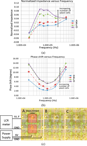
Impedance spectroscopy measurements on TFT array substrates have been performed for frequencies from 1 kHz to 2 MHz. The purpose here was to investigate the possibility of monitoring the growth of cells during their culture on TFT array substrates. An increase in the impedance with the number of cells was expected. Actually, if the number of cells on an electrode increases, the effective electrode area is reduced, which increases the impedance across the electrode. Here too, yeast cells were used to investigate the possibility of impedance spectroscopy with TFT array substrates. Cell culture growth was simulated by performing DEP to accumulate cells at the level of the measurement electrodes.
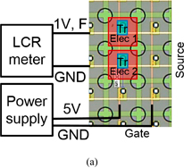
Figures 6(a) and 6(b) shows respectively the measurement setup and the corresponding equivalent circuit used for impedance spectroscopy measurement of yeast cells in DIW. A DC power supply of 5 V was applied to two neighboring gate lines, while an Agilent E4980A LCR meter was connected to two neighbor source lines, on which an AC signal of 1 V with a frequency ranging from 1 kHz to 2 MHz was applied. The measurement was performed between the two electrodes, which are in red in the figure and are named "Elec 1" and "Elec 2". The TFTs of these two electrodes are shown in blue and are named "Tr". Some rounded structure can be seen at the corners of the electrode. These are structures fabricated underneath the ITO electrodes for other purposes, and do not have any influence on the impedance measurements. Thus they are neglected in this section.
Download figure:
Standard image High-resolution image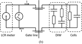
Fig. 6. (a) Measurement setup and (b) equivalent circuit for the impedance measurement. (a) The ITO microelectrodes on the substrate appear in gray color and are square. The circles on the substrate correspond to insulator patterns which were fabricated under the ITO microelectrodes but do not have any influence on the measurement.
Download figure:
Standard image High-resolution imageFigures 7(a) and 7(b) respectively show the variation of the normalized impedance and the variation of the phase shift obtained from the impedance data of DIW when the number of yeast cells between the electrodes is increasing. The variation of the normalized impedance was obtained by calculating the difference between the impedance with cells and without cells (only DIW), and dividing it by the impedance without cells. At around 100 kHz, a clear variation of the impedance of 10 mΩ order was observed with increasing number of the cells. This is why we have only shown the impedance for frequencies between 10 kHz and 1 MHz for better visualization of the results. These results show that the impedance as well as the phase increase with the number of yeast cells. This is due to the fact that at this frequency, cells act as an insulating layer owing to their lipid membrane, which is opaque to the electric field. The results are similar to those obtained in other publications.37) The yeast cells accumulated at the level of the measurement electrodes, as shown on Fig. 7(c), when using DEP, imitating cell multiplication during a culture. Accumulation can be easily obtained because the frequency range of the measurement is the same as that required for the DEP of yeast cells: around 100 kHz. To avoid DEP when measuring, a short measurement time can be applied, as DEP is a relatively slow process.
Fig. 7. Results of impedance measurements. (a) Variation of normalized impedance with the concentration of yeast cells. (b) Variation of phase with the concentration of cells. (c) Photographs of the measurement area with increasing concentration of cells. The cells accumulate by DEP.
Download figure:
Standard image High-resolution image
These results show that impedance spectroscopy measurements on TFT array substrates are possible. It should be possible to use this technique to monitor cell cultures on TFTs. However, additional experiments have to be carried out in order to provide more quantitative results related to the number of yeast cells.
6. Discussion
The different experiments described in the last section were performed to investigate the possibility of using TFT array substrates as platforms for electrical experiments on biological cells, as well as to investigate the possible areas of application of such substrates.
Compared with MEA and CMOS devices, TFT array substrates have the advantage of 80% transparency, a density of microelectrodes as high as 82%, and the possibility of coverage with independent microelectrodes as large as standard Petri dish boxes or 96-well plates. Owing to the high density of microelectrodes, alignment is no longer necessary between cells and microelectrodes as microelectrodes are everywhere and almost any cell on the surface is in contact with a microelectrode. In addition, the successful culture of different types of cells, such as fibroblasts, primary chick brain cells, and liver cells, showed the biocompatibility of the substrate. Finally, successful fluorescence observation and microfluidic attachment demonstrated the optical and microfluidic compatibility of such substrates. Thus, from the structural and dimensional viewpoints, TFT array substrates are very interesting and perfectly compatible with standard cell biology experiments.
From the electrical viewpoint, TFTs are fabricated to be used in DC mode. Thus, the DC usage of the microelectrodes is straightforward, allowing them to be used in ISFETs for instance. Actually, because TFTs are transistors, they can be used as ISFETs to sense the pH or ion activity of cells for instance. This aspect is under study by our group.
In parallel, many electrical experiments on biological cells use electrical pulses or an AC signal, such as those involving the electrical excitation of neurons,11) electroporation,41) DEP,42) and impedance spectroscopy.35) This is why the AC usage on the microelectrodes is particularly essential. When characterizing microelectrodes in AC, clear attenuation at frequencies above 1 kHz appeared. This attenuation might adversely affect experiments on biological cells due to the possible insufficient amplitude of the signal. However, despite this concern, the results obtained for the manipulation of cells by DEP and impedance spectroscopy demonstrated that AC electrical experiments are possible with such substrates.
From the results obtained, it can be concluded that such substrates can be used with frequencies under 1 MHz. In particular, the placement and separation of cells by DEP, at least for frequencies up to 100 kHz, have been demonstrated. Impedance spectroscopy to monitor cell culture growth has also been demonstrated, and other applications, such as the monitoring of cell viability and cell attachment, are under investigation.
Pulsed signals also have many applications to the study of biological cells. We are also investigating this area with the aim of performing the electroporation of cells and cell excitation, particularly for neuron excitation. However, for these types of signals, which usually have a low frequency of under 1 kHz, some problems of damage to ITO microelectrodes have already been observed. We are now working to solve this problem.
Regarding the development of an electrical platform for biomedical applications, such as the study of motor neuron/muscle cell interactions in the case of ALS disease, the results obtained demonstrate the possibility of monitoring cell culture growth on such a platform and cell placement. It is also predicted that all experiments involving lower frequencies should be possible, especially neuron excitation and activity recording, which are essential tool, in experiments on neurons.
7. Conclusions
In this article, we discussed the possibility of using TFT technology for experiments on biological cells. A detailed background on the history of TFT technology development and common applications such as LCDs, X-ray detection, pressure sensing for touch panel displays, IR sensing, and chemical and biochemical sensing has been given.
An area of research has never been, to our knowledge, investigated with this technology: the use of TFT array substrates to perform the electrical excitation, manipulation, and sensing of biological cells. These substrates have many advantages compared with those fabricated with more standard technologies such as MEA and CMOS technologies. TFT array substrates are large transparent electroactive substrates with a dense array of transparent microelectrodes that are individually controllable. Such substrates are very attractive for biological applications with cells as they also allow optical observation as well as electrical interactions with cells without the need for alignment between cells and microelectrodes. They are similar to advanced MEA devices.
Our aim is to develop a platform with TFT array substrates for the biomedical study of motor neuron/muscle cell interactions that occur in ALS disease. To develop this platform, the monitoring of cells growth and the possibility of cell excitation and recording are essential.
Several experiments have been performed on a TFT array substrate, removed from a smart phone screen toward achieving this aim and to investigate the possibility of using it as a platform for biomedical applications. Characterization of the transistors with an AC signal showed clear attenuation of the signal above 1 kHz. Despite this attenuation, experiments on dielectrophoresis for cells placement on the substrate and on impedance spectroscopy to monitor cell culture growth were successfully performed at frequencies around 100 kHz.
Thus, it can be concluded that TFT array substrates can be used for frequencies under 1 MHz. This is a sufficiently large range of frequencies to perform experiments on dielectrophoresis and impedance spectroscopy. Other experiments that require the use of pulses such as neuron cell excitation and cell electroporation are under way. These experiments are providing very promising results and demonstrate the possibility of using TFT array substrates as platforms for the biomedical investigation of cells.
Acknowledgements
This work was partially supported by advice and microprocessing by VDEC and the NanoTech Platform at the University of Tokyo.