
Abstract
This review article focuses on the development of processes for the manufacture of organic electronic circuits. Beginning with the first report of an organic transistor it highlights the key developments leading to the successful manufacture of microprocessors and other complex circuits incorporating organic transistors. Both batch processing (based on silicon integrated circuit technology) as well as mass-printing, roll-to-roll (R2R) approaches are discussed. Currently, the best circuit performances are achieved using batch processing. It is suggested that an emerging, large mass-market for electronic tags may dictate that R2R manufacture will likely be required to meet the high throughput rates needed. However, significant improvements in resolution and registration are necessary to achieve increased circuit operating speeds.
Export citation and abstract BibTeX RIS
1. Introduction
Considerable progress is being made towards the commercialization of organic electronics. The major success story to date is the organic light emitting diode (OLED), first reported by Tang and VanSlyke1) in 1987. OLEDs are now well-established in a variety of displays but usually driven by a silicon backplane. The commercialization of organic electronic circuits, now often subsumed into plastic, printed or flexible electronics, has been slower. Nevertheless, the promise of low-cost organic thin film transistor (TFT) production onto flexible substrates, with the latter providing opportunities for achieving products with different form factors, continues to drive research and development into improved manufacturing routes for organic electronic circuits. One of the early goals was the replacement of silicon backplanes in displays, but metal oxide TFT technology2) is now overtaking organics for this role. Until a reliable, low-temperature, solution processable oxide technology for plastic film substrates is developed, organics may still have a significant part to play in this domain. Other achievable goals for organic electronics include radio-frequency identification tags for product tracking and security branding, wearable electronics, logic and analogue circuits for disposable multi-analyte sensors as well as biomedical applications. The "Internet of Things" is also opening new avenues of exploitation with the possibility of flexible integrated circuit tags being embedded in a wide range of mass-market objects that can be interrogated by near-field communication systems.3)
This article provides a brief review of the progress being made towards the commercial production of organic electronic circuits, beginning with an overview of some of the key, early reports before proceeding to discuss recent developments in roll-to-roll (R2R) and batch production approaches for fabricating such circuits.
2. Early developments
Field-effect measurements on organic materials were undertaken as early as 1971 by Bauser and Pernisz4) who used an electrode above an anthracene crystal to modulate the surface current along the crystal. Although the aim of the measurements was to investigate surface states on the anthracene crystal, the experimental arrangement acted as a crude field-effect transistor with air as the gate dielectric. Despite this early demonstration, it was not until 1987 that Koezuka et al.5) reported the first working organic field-effect transistor (OFET).
As in many later works, the substrate was oxidized silicon, which acted both as a gate electrode and gate dielectric. Gold source and drain electrodes were deposited onto the oxide with the semiconductor, polythiophene, electrodeposited over the electrodes and into the channel thus forming a bottom-gate, bottom-contact transistor (inset Fig. 1). The output characteristics of the resulting device, shown in the main figure, display good saturation and clear control of the device current by the applied gate voltage. The slight non-linearity in the characteristics at low drain voltage suggests the presence of contact effects, which can be expected in this TFT configuration. It may, in part, account for the relatively low hole mobility, 2 × 10⁻⁵ cm2 V−1 s−1, measured in the device, compared with 8.5 × 10⁻⁴ cm2 V−1 s−1 reported a few years later6) for a similarly fabricated device based on poly(3-methylthiophene).
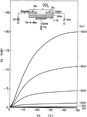
Fig. 1. Output characteristics of the first organic field-effect transistor. The transistor had the bottom-gate, bottom-contact structure (see inset). Electropolymerisation of polythiophene over the source and drain electrodes caused the polymer to spread into and fill the channel region above the SiO2 gate dielectric. Reprinted with permission from Ref. 5. © 1987 Elsevier B.V.
Download figure:
Standard image High-resolution imageIn the same period, a number of laboratories7,8) were spin-casting polymers such as poly(3-hexylthiophene), P3HT, and reporting hole mobilities in the range up to ∼10−4 cm2 V−1 s−1. Sirringhaus et al.9) have since demonstrated hole mobilities as high as 0.1 cm2 V−1 s−1 in P3HT-based TFTs. More recently, mobilities well in excess of 1 cm2 V−1 s−1 have been achieved in TFTs formed from solution-processed blends of small molecules in a host polymer.10,11)
Some years later Garnier and co-workers showed that TFTs could be fabricated from π-conjugated small molecule acenes and thiophenes12,13) with reported mobilities ∼0.05 cm2 V−1 s−1. A key milestone was reached in 1997, when Lin et al.14) reported bottom-gate, top-contact, evaporated pentacene TFTs with mobility ∼0.6 cm2 V−1 s−1. The ability to fabricate OTFTs with mobilities comparable to amorphous silicon (∼1 cm2 V−1 s−1) showed that organic materials had the potential to replace silicon in many applications, including display backplanes. As will be discussed later, organic materials with even higher mobilities have been reported since then, including n-type materials for use in complementary circuits.
Reports of organic integrated circuits began to emerge around the turn of the century, the first being a solution-processed, all-polymer 15-bit decoder (Fig. 2) fabricated by the Philip's group.15,16) This was followed rapidly by complementary circuits such as shift registers demonstrated by Crone et al.17) Using a precursor pentacene route for semiconductor deposition, Gelinck et al.18) were able to demonstrate a 64 pixel × 64 pixel electrophoretic display and a 32-stage shift register requiring 1,888 operational TFTs. Someya and his team in Japan developed the idea of large-area organic electronics. They demonstrated the concept by creating artificial skin using a rubber pressure pad connected to a TFT addressable array.19,20) Such demonstrations provided a strong stimulus for further research and development into better materials and improved production methods for OTFTs and circuits, which have been described in several recent books.21–23)

Fig. 2. A 15-bit mechanically programmable code generator fabricated by Philips is an early example of an all-polymer integrated circuit. Reprinted with permission from Ref. 15. © 1998 AIP Publishing LLC.
Download figure:
Standard image High-resolution image3. Manufacturing processes
3.1. General principles
The general criteria determining the eventual design of organic TFTs are readily derived from the standard equations describing the current ID flowing from source to drain electrodes, i.e.,
in the linear regime and
in saturation. Here W and L are the channel width and length respectively, μ the mobility, Ci the capacitance per unit area of the gate dielectric, and VD, VG, and VT the drain, gate, and threshold voltages, respectively. From these we may identify two important materials related parameters, namely, the carrier mobility μ in the semiconductor and the dielectric constant, εr, of the gate dielectric which together with di, the dielectric thickness determines its capacitance per unit area, Ci (= εrε0/di with ε0 the permittivity of free space). The combination of semiconductor and dielectric used also implicitly determines VT, through (i) the morphology-dependence of the density of states in the semiconductor near the interface and (ii) carrier trapping states in the insulator at or near the interface.
In many research studies pentacene, a p-type semiconductor, has been the active material of choice. Recently, though, as a consequence of their higher mobility and better environmental stability dinaphthothienothiophene (DNTT)24–26) and its soluble analogue C10-DNTT27) have become more widely used. Also emerging are high-mobility n-type organic materials, e.g., naphthalene diimide,28) a necessary development for implementation of organic complementary circuits.
While much early work utilised SiO2 as the gate dielectric, a wide range of alternative materials have been investigated.29) Ideally, Ci should be as large as possible which can be achieved using thin films with high dielectric constant. However, polar surfaces are generally incompatible with high mobility owing to dipolar dispersion.30) Often, therefore, a bilayer dielectric is used in which case a high dielectric constant layer is coated with a low polarity material. Examples include aluminium oxide covered in a self-assembled monolayer (SAM)31) or capped with a styrene based polymer.32) Also reported are polystyrene-capped nanocomposite films of poly(vinyl phenol) and barium titanate.33)
While ID depends explicitly on the channel dimensions W and L, other important dimensions include the thickness of the semiconductor layer and the degree to which it extends beyond the channel width W. These can lead to parasitic source–drain currents that add to both the off- and on-currents in the TFT, the latter leading to over-estimate of carrier mobility.34)
Any manufacturing process must, therefore, be able to deposit or create patterned layers of metal, semiconductor and insulator of the relevant dimensions — ideally L < 5 µm and di < 500 nm. This is exemplified in the diagrams in Fig. 3 which show (a) cross-section and (b) plan views of a bottom-gate top-contact OTFT. Additive printing of the necessary materials is preferred as it results in less material wastage and eliminates the need for post-deposition patterning. In principle, additive printing can also overcome the need to create the vias in pre-deposited films required for connecting lower level conducting tracks to upper level tracks as seen in the cross-section diagram [Fig. 3(d)] of the enhancement load inverter in Fig. 3(c). As more complex circuits are built, it becomes necessary also to connect VOUT from one stage to VIN of another, which again requires connection through a via in the semiconductor and dielectric layers.
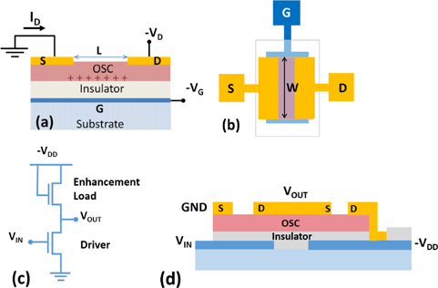
Fig. 3. Diagrams of (a) the cross-section and (b) plan views of bottom-gate, top-contact OTFT. In (b) the organic semiconductor (OSC) is patterned to avoid parasitic source–drain currents outside the channel area. (c) Circuit diagram of a unipolar, enhancement load inverter and (d) cross-sectional diagram of the fabricated structure.
Download figure:
Standard image High-resolution image3.2. R2R processing
Organic electronics has long been associated with low-cost, low-temperature fabrication of circuits on flexible substrates using one or more of several commercial methods such as inkjet, gravure, flexographic and screen printing. Other applicable methods include slot-dye and spray coating, organic vapour jet printing and micro-contact printing. Reviews35,36) of these various methods for fabricating OFETs were published recently. Here we concentrate mainly on the production of functional circuits.
Inkjet printing was an early candidate for the manufacture of high-resolution circuits with the demonstration of an inverter operating at several hundred Hz.37) In this case only the electrodes were printed. The semiconductor and dielectric layers were spin-coated with vias created by localised printing of the solvent for the dielectric.38) Later workers39,40) used a combination of inkjet and gravure printing to fabricate their OTFTs while Chung et al.41) demonstrated a fully inkjet production process. Using a combination of inkjet and screen printing, Verihlac et al.42) reported a 5-stage ring oscillator operating at 300 Hz. More recently, Kjellander et al.43) inkjet-printed TIPS-pentacene onto a pre-patterned bottom-gate, bottom-contact transistor template, thereby realising a 19-stage ring oscillator operating at 500 Hz.
While inkjet printing can achieve high resolution, printing speeds are generally low. In mass-printing processes, a trade-off can be made between resolution and printing speed. For example, Hübler et al.44) used a combination of offset, gravure and flexographic printing at a web-speed of 60 m/min to realise a 7-stage ring oscillator. However, the poorer resolution (L = 100 µm) led to a much lower operating frequency, ∼4 Hz. Using single-walled carbon nanotubes as the active semiconductor, Noh et al. were able to produce a range of fully operational gravure-printed circuits with L = 170 µm. These included a half adder, full adder and D-flipflop,45–47) albeit operating with stage delays longer than 10 ms.
Recently, a strong case was made for R2R fabrication of organic circuits using vacuum-evaporation methods only, thereby avoiding the use of solvents.48,49) It was argued that the printing of fine metal lines is already a commercially-used, high-speed R2R production process.50,51) Systems for rapid deposition of active layers in organic light emitting diodes using organic vapour phase deposition (OVPD) are also well-advanced.52) Furthermore, OVPD has been used for OFET production53) and may be combined with high-resolution masks for patterning structures54) or, alternatively, a small-diameter vapour jet used for local deposition of the semiconductor.
For the dielectric layer, Abbas et al.55) adapted a commercial route used for depositing polymeric coatings onto moving plastic webs. They based their approach on the vacuum-evaporation and in-situ polymerisation of the monomer tripropyleneglycol diacrylate (TPGDA) as the gate dielectric. Combining the dielectric process with evaporated films of DNTT, the group demonstrated a high transistor yield (∼90%), from a vacuum-evaporation process operating in a R2R-compatible environment.56) The method was used successfully to demonstrate 5-stage ring oscillators operating at ∼2 kHz26) corresponding to a stage delay ∼50 µs, using TFTs with channel lengths of 50 µm. Although requiring the application of a thin polystyrene buffer layer on the TPGDA to achieve device stability by reducing dielectric surface polarity, this represented a major advance over circuits produced entirely by mass-printing methods. Also reported were a range of logic gates [inverters, NOR and NAND gates, and a Set–Reset (S–R) latch] and a current mirror circuit.57) With little or no recourse to the use of solvents, the vacuum-route to R2R has many attractions. Many problems such as low carrier mobility, poor dielectric properties and low yield in mass-printing processes are directly related to solvent use. Vacuum-compatible approaches to buffering the dielectric surface are being developed by the group who have also reported more rapid deposition of the semiconductor onto localised areas using OVPD.56)
Further performance improvements could be readily achieved using the vacuum evaporation route described above. For example, improving the resolution and registration ability that is currently achievable in the high-speed metal patterning process would allow significant improvement in transistor performance. In principle, reducing the channel length from 40 to 10 µm could, potentially reduce the stage-delay by an order of magnitude, with further improvement possible by reducing parasitic gate-to-source and gate-to-drain overlap capacitances.26)
As will be seen in the next section, these are the prime reasons for the significantly better performance of batch-produced circuits using processes derived from silicon device manufacture.
3.3. Batch processing
Batch processing is inherently a slower process than R2R production. However, this is compensated by significant improvement in TFT performance and considerable increase in the circuit complexity that is possible. The technology is based on that used for silicon integrated circuit production. For processing flexible plastic substrates, e.g., polyimide, poly(ethylene naphthalate), or poly(ethylene terephthalate), the plastic film is laminated onto a silicon wafer or other suitably rigid carrier and delaminated after processing is complete. Generally, bottom-gate architecture is favoured (see inset Fig. 1) with gold or aluminium gate electrodes formed by photolithography. The gate dielectric may be a spin-coated and UV-photopatterned polymer film58) or a sputtered aluminium oxide layer coated in a SAM layer59) to achieve lower voltage operation, although not as low as achieved by Zschieschang et al.25,27) using thinner electrolytically grown oxide layers. Gold source and drain electrodes are photolithographically patterned on the dielectric. Finally, the semiconductor is deposited from (i) a solution-processed pentacene precursor,58) (ii) by thermal evaporation of pentacene,59) or (iii) by inkjet printing a soluble small molecule such as TIPS-pentacene.43) Isolation of TFTs to minimise parasitic effects can be achieved by exposure to an oxygen plasma through an appropriate shadow mask60) or by containing the active semiconductor within areas defined by an integrated photoresist shadow mask.59)
Following the demonstration of an electrophoretic display and 32-stage shift register by the Philips group in 2004,18) a steady stream of publications emerged. Examples include the 2007 report by Cantatore et al.58) of an RFID transponder capable of reading a 64-bit tag at a data rate of 150 bits/s. In 2010, Myny et al.59) reported an 8-bit RFID transponder chip based on 2 µm design rules which provided a data rate of 50 kbps compatible with Electronic Product Coding and with a rail voltage of just 18 V.
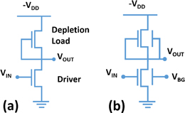
The particular problem posed by many but not all OTFTs is the positive threshold voltage which results in significant drain current when VG = 0 V. Consequently, inverters necessarily are designed with the load transistor operating in the depletion (VGS = 0 V) mode i.e., gate electrode connected to the source as in Fig. 4(a) rather than the drain electrode as in Fig. 3(c). Including a second or back-gate in the pentacene TFT, as shown in Figs. 4(b) and 4(c), allows VT to be controlled over a wide range61–63) with the added advantage of increasing the noise margin of the inverter. Using this approach, Myny et al.63) built an 8-bit, 40 instructions/s microprocessor (see Fig. 5) operating from a supply voltage of 10 V and a back gate voltage of 50 V. They demonstrated that the microprocessor was capable of executing the multiplication of two 4-bit numbers.
Download figure:
Standard image High-resolution image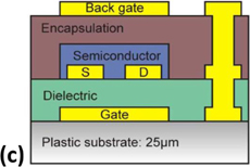
Fig. 4. (a) Single and (b) dual gate, unipolar depletion load inverter. (c) Cross-section of a dual gate organic TFT. Reprinted with permission from Ref. 63. © 2012 IEEE.
Download figure:
Standard image High-resolution image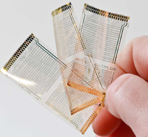
Fig. 5. Photographs of 8-bit microprocessors fabricated on flexible foil. Reprinted with permission from Ref. 63. © 2012 IEEE.
Download figure:
Standard image High-resolution imageIn a later publication3) a similar microprocessor was demonstrated, but this time based on complementary logic (organic p-type and oxide n-type semiconductors). Also by including a write-once-read-many (WORM) instruction generator, the microprocessor could be made "application specific" simply by inkjet printing silver ink into wells to complete the connections to input and load TFTs in the instruction generator (Fig. 6).

Download figure:
Standard image High-resolution image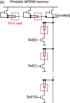
Fig. 6. (a) Block diagram of the instruction generator used for programming the multi-input NAND WORM memory for an application specific microprocessor. (b) The memory is programmed by inkjet printing silver ink into the print wells to complete the required connections. Additional load TFTs can be included in the circuit depending on the number of input TFTs utilised. Reprinted with permission from Ref. 3. © 2014 Macmillan Publishers Ltd.
Download figure:
Standard image High-resolution imageThis move towards application specific integrated circuits is also the theme of the recent report by Sou et al.64) who demonstrated a programmable logic array based on Plastic Logic's backplane technology. In this case, silver wire connections and poly(3,4-ethylenedioxythiophene):poly(styrene sulfonate) (PEDOT:PSS) resistors were inkjet-printed between OTFTs or logic blocks to achieve particular electronic functionality e.g., multiplexing.
4. Future perspective
From the foregoing, it is clear that by adopting a batch processing approach, electronic circuitry can now be manufactured with sufficient functionality for a range of applications. Evaporable and solution processable semiconductors such as C10-DNTT are available with significantly higher mobility than pentacene suggesting that even better performance is within reach simply by changing the active semiconductor. The major challenge for this approach now lies in upscaling to meet the potentially large market resulting from the electronic labelling of mass consumer goods when the "Internet of Things" becomes fully realised. To meet the demand, increases in throughput rate must be achieved while retaining high yield and reducing production costs.
In principle, R2R manufacture has the capability of meeting high throughput rates at low cost. After all, this is the basis of most printed packaging operations and was a major driver for printed electronics. To date, however, the performance of devices and circuits produced by mass-printing methods lags far behind that achievable by batch processing. Improvements in resolution and registration, both of which can be achieved by reducing web speed, could lead to the production of circuits with sufficient functionality for some applications.
While batch processing lends itself to wafer or sheet level testing during production, this poses a major challenge for R2R manufacture. Any manufacturing errors must be identified rapidly and corrected "on the fly" before major production losses occur. There is a need, therefore, for methods that allow rapid evaluation of film quality, pattern definition and device functionality. Optical techniques are probably best suited for such applications and can range from direct visual inspection of patterned layers to electro-optical techniques based on, for example, charge-induced changes in reflectance spectra65–67) for visualising active channels in TFTs.
In general, preparing dielectric and semiconducting layers using vacuum-based processes result in higher mobility devices produced at higher yield. Already good progress has been made in fabricating circuits in a vacuum R2R environment26,48,49,55–57) with higher mobilities giving considerably better circuit performance than that achieved by all mass-printing (solution process) methods. With routes to further significant improvements already identified49) vacuum-R2R-processing is certainly worthy of further research and development effort.
Nanoimprint lithography (NIL) is a R2R-compatible processing route that can provide a route to TFTs meeting submicron design rules68–70) while solvent-soaked stamps could be used for removal of material to create vias.71) Whether NIL stamps can be maintained in pristine condition during continuous use is open to question, suggesting that the approach may be more suited to batch production.
The biggest challenge to organic electronics comes from metal oxide semiconductor technology which, until recently, had been hampered by (a) the need for high temperature processing to achieve high mobility TFTs and (b) the lack of stable p-type material. The first restriction can be overcome to a degree by trading-off performance against processing temperature. While some p-type oxides are now becoming available, stability is still an issue. This deficiency affords an opportunity for p-type organics in hybrid oxide/organic complementary technology as demonstrated effectively by Myny et al.3) With stable, high mobility n-type organic semiconductors becoming available, an all-organic complementary technology is also practical.72)
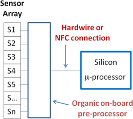
Other opportunities for organic electronics lie in, for example, integrated sensor systems where data from multi-parameter sensors can be pre-processed by an on-board organic microprocessor prior to transmission via a hardwire or wireless link to a server (Fig. 7). Such systems will require fabrication of analogue circuits, for example, comparators (for which current mirror sources are essential57)) and differential amplifiers, a strategy for which has already been demonstrated.73) With considerable effort being directed towards using organic electronics in biomedical applications74,75) multi-sensor systems with on-board data processing could prove particularly useful.
Fig. 7. Schematic of a multisensory array. The on-board data-preprocessor undertakes initial data analysis prior to transmission to the main control computer via a hardwire or near-field communication (NFC) connection.
Download figure:
Standard image High-resolution image
5. Conclusions
Organic electronics has come a long way since the first report of an organic transistor in 1987. Clear routes to batch production are now in place. Although current R2R routes for continuous production still lag behind in terms of achievable circuit performance, sufficient progress has been made in the last 5 years or so to suggest that by improving resolution and registration, useful circuits could be manufactured at moderately high speed. The "Internet of Things", nano-imprint lithography and biomedical applications will act to stimulate further activity worldwide. While challenges do remain, a commercially successful organic integrated circuit technology is becoming a reality.