
Abstract
Cu2ZnSn(S,Se)4 (CZTSSe) solar cells are fabricated with CdS and (Cd,Zn)S buffer layers of different thicknesses to investigate sputtering damage on the absorber surfaces during ZnO:Al/ZnO layer deposition. In this work, the sputtering damage is scrutinized by photoluminescence (PL) measurement. The damage (i.e., non-radiative recombination centers) near the absorber surfaces investigated on the basis of PL peak intensity decreases with increasing thickness of the buffer layer. Furthermore, the intensity in the solar cells with the CdS buffer is higher than that with the (Cd,Zn)S buffer layer, suggesting that the CdS buffer layer demonstrates better capability of preventing sputtering damage near the CZTSSe surface than the (Cd,Zn)S buffer. PL ratio defined as the ratio of the PL peak intensity after sputtering to the PL peak intensity before sputtering is utilized to quantify sputtering damage. The solar cell performance increases with increasing PL ratio up to 0.5, followed by saturation at a ratio higher than 0.5. Taken together, PL ratio is proposed as a tool for monitoring sputtering damage for improving cell performance.
Export citation and abstract BibTeX RIS
1. Introduction
Recently, the Cu(In,Ga)Se2 (CIGS) solar cell with an efficiency of over 20% has been realized by several groups; this solar cell is one of the thin-film solar cells with the highest efficiency.1–5) It has several advantages such as long-term reliability and radiation durability.6,7) CIGS includes indium (In), which is a rare metal. This makes it difficult for the CIGS solar cell to meet the drastically increasing demand of photovoltaic market worldwide. Therefore, In-free solar cells have been studied. One of the In-free solar cells is the Cu2ZnSn(S,Se)4 (CZTSSe) solar cell, which is composed of Cu2ZnSnS4 [band-gap energy (Eg) of 1.5 eV] and Cu2ZnSnSe4 (Eg of 1.0 eV).8–10) The CZTSSe solar cell has a conversion efficiency of over 30% theoretically.11) To date, the highest conversion efficiency of the CZTSSe solar cell is 12.7%,12) which is much lower than that of the CIGS solar cell. Research on the fabrication technology for the CZTSSe solar cell is accordingly conducted to improve its performance.13–16) CdS layers, which are deposited by chemical bath deposition (CBD), are normally utilized as buffer layers in the CZTSSe and CIGS solar cells.1,2,5,12–19) This is because the conduction band offset (CBO) of the CdS/CIGS interface is appropriate,20–22) and CdS can form high-quality-p–n junctions of the solar cells owing to the prevention of sputtering damage on the absorber surface during ZnO:Al(AZO)/ZnO fabrication.23,24) Nevertheless, the CdS buffer layer absorbs light with a wavelength shorter than 520 nm because its Eg is 2.4 eV.25) Therefore, the CZTSSe solar cell losses current owing to light absorption in the CdS buffer layer of 50–70 nm thickness.13,14,17–19) To eliminate this problem, thin CdS buffer and/or wide Eg buffer layers, such as Zn(O,S),26) (Zn,Mg)O,27) and (Cd,Zn)S, are used. (Cd,Zn)S has already been used in the CIGS solar cell,28,29) where its deposition process is the same as CdS fabrication.
In this work, thin CdS and (Cd,Zn)S buffer layers were deposited on CZTSSe solar cells. It is found that the sputtering damage near the surface of the CZTSSe absorber is formed after AZO/ZnO fabrication in spite of the presence of a thin CdS or (Cd,Zn)S layer on the absorber surface, thereby decreasing conversion efficiency. The sputtering damage was thus characterized by photoluminescence (PL) measurement.
2. Experimental methods
In this work, the structure of the CZTSSe solar cell is Al/AZO/ZnO/buffer layer/CZTSSe absorber/Mo/soda-lime glass (SLG) substrate. The samples of CZTSSe/Mo/SLG were fabricated by Solar Frontier. In their fabrication, after preparing a Mo layer as a back contact on an SLG substrate, a CZTSSe layer was deposited. First, metallic precursors were deposited on Mo-coated SLG substrates. The CZTSSe layers were then formed by sulfurization and selenization to the precursors.30) The Eg of the resulting CZTSSe layers in this work was constant at 1.08 eV, as calculated from external quantum efficiency (EQE). After the formation of the CZTSSe layers on the Mo-coated SLG substrates, HCl (1 M, 1 min) and KCN (1 wt %, 1 min) etchings were subsequently conducted at room temperature in order to remove impurities from the CZTSSe surface, where the impurities become shunt paths.31) The samples were successively annealed at 150 °C for 30 min in N2 atmosphere to decrease the density of defects acting as non-radiative recombination centers, which was observed in our previous work.32) The buffer layers in the CZTSSe solar cells were CdS and (Cd,Zn)S. The CdS growth solution was composed of CdSO4 + 8/3 H2O (1.125 mM), ammonia (2.368 M), and thiourea (56.25 mM), whereas the (Cd,Zn)S growth solution consisted of CdSO4 + 8/3 H2O (1.5 mM), ZnSO4 (7 mM), ammonia (0.37 M), and thiourea (50 mM). The CdS and (Cd,Zn)S buffers were next deposited by chemical bath deposition at 80 °C. The thicknesses were controlled by deposition time. The Eg values of CdS and (Cd,Zn)S were 2.38 and 2.58 eV, respectively. We also fabricated the CZTSSe solar cell without a buffer layer to compare with the cell with a buffer layer. After the buffer deposition, 50-nm-thick ZnO as a window layer and 300-nm-thick AZO as a transparent conductive oxide (TCO) were deposited by RF magnetron sputtering at a back pressure of 5 × 10⁻⁴ Pa. The working pressures of 0.25 and 0.4 Pa as well as RF powers of 50 and 110 W were used for the fabrication of ZnO and AZO, respectively. The target diameters of ZnO and AZO were 76.2 mm. Finally, front grids of Al were deposited by vacuum thermal evaporation. The active area of the solar cells was 0.24 cm2.
Current density–voltage (J–V) characteristics of the CZTSSe solar cells were measured under AM 1.5G illumination (100 mW/cm2) at 25 °C. EQE measurement in a range from 300 to 1300 nm was performed by two-source illumination (xenon and halogen lamps) using a rock-in detection system. After EQE measurement, internal quantum efficiency (IQE) was calculated using EQE/(1 − R), where R denotes the reflectance of the cell with the structure of AZO/ZnO/buffer layer/CZTSSe/Mo/SLG.
PL was furthermore measured utilizing a 532 nm laser with a pulse width less than 1 ns and at a repetition rate of 15 kHz. The average power density of the excitation laser was 1.87 mW, and the laser beam had an ellipse-shaped spot of 0.8 mm width and 1.0 mm height. The laser power was nearly identical to the number of photons entering the CZTSSe absorber with Eg of 1.05 eV under AM 1.5G illumination. Figure 1 shows the process of preparing the samples for PL measurement to evaluate the sputtering damage near CZTSSe surfaces caused by AZO/ZnO fabrication. As shown in the figure, the PL spectrum of the bare CZTSSe absorber in Fig. 1(a) was first measured. This PL spectrum is called the "PL spectrum before sputtering" and the PL peak intensity is called the "PL peak intensity before sputtering". Then, the buffer, window, and TCO layers were fabricated on the CZTSSe absorber to measure solar cell parameters, as shown in Fig. 1(b). Next, the buffer, window, and TCO layers were removed from the solar cell, as shown in Fig. 1(c), by HCl etching to measure the PL spectrum of the CZTSSe absorber. This PL spectrum is called the "PL spectrum after sputtering" and the PL peak intensity is called the "PL peak intensity after sputtering". The PL ratio was therefore defined as the ratio of the PL peak intensity after sputtering to the PL peak intensity before sputtering.

Fig. 1. Process of preparing the samples for PL measurement to evaluate the sputtering damage near CZTSSe surfaces caused by AZO/ZnO fabrication.
Download figure:
Standard image High-resolution image3. Results and discussion
Figure 2 shows the photo-J–V characteristics of the CZTSSe solar cells without the buffer layer as well as those with the 10-nm-thick CdS and 10-nm-thick (Cd,Zn)S buffer layers. Table I shows photovoltaic performance characteristics, corresponding to the J–V characteristics shown in Fig. 2. It is revealed that a short-circuit current density (JSC) of 37.5 mA/cm2 for the solar cell with the CdS buffer layer is higher than that with the (Cd,Zn)S buffer layer. The lowest JSC for the solar cell without the buffer layer is possibly attributed to the sputtering damage on the absorber surface. Figure 3 shows the IQEs of the corresponding CZTSSe solar cells shown in Fig. 2. The IQEs of approximately 400–900 nm are markedly affected by the buffer layer. The highest IQE in this range is observed in the cell with the CdS buffer layer, thus leading to the highest JSC, whereas the lowest is observed in the cell without the buffer layer. It is considered that the different IQEs in the range of about 400–900 nm shown in Fig. 3 are attributable to the different capabilities of the buffer layers to prevent the sputtering damage on the absorber surface after AZO/ZnO deposition. Therefore, it is intriguing to characterize the damage in the cells without buffer layers and in the cells with the CdS and (Cd,Zn)S buffer layers by PL measurement, which is a fast and non-destructive method.
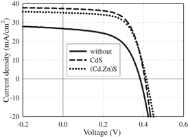
Fig. 2. Photo-J–V characteristics of the CZTSSe solar cells without and with 10-nm-thick CdS and 10-nm-thick (Cd,Zn)S buffer layers.
Download figure:
Standard image High-resolution imageTable I. Solar cell performance characteristics of the CZTSSe solar cells with different buffers.
| Buffer layer | JSC (mA/cm2) | VOC (V) | FF (%) | η (%) | RS (Ω cm2) | RSh (kΩ cm2) |
|---|---|---|---|---|---|---|
| Without | 26.7 | 0.384 | 56.4 | 5.79 | 0.512 | 0.178 |
| CdS | 37.5 | 0.408 | 64.0 | 9.77 | 0.477 | 0.437 |
| (Cd,Zn)S | 34.7 | 0.415 | 62.7 | 9.04 | 0.959 | 0.240 |
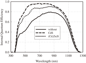
Fig. 3. IQEs of the CZTSSe solar cells without and with 10-nm-thick CdS and 10-nm-thick (Cd,Zn)S buffer layers.
Download figure:
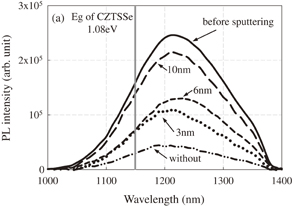
Standard image High-resolution imageFigure 4(a) shows the PL spectra after sputtering (dash lines) of the solar cells without buffer layers and those with CdS buffer layers of 3, 6, and 10 nm thicknesses and the PL spectrum before sputtering (solid line). Similarly, Fig. 4(b) shows the PL spectra after sputtering (dash lines) the cells without and with the (Cd,Zn)S buffer layers of 3, 6, and 10 nm thicknesses and the PL spectrum before sputtering (solid line). It is revealed that all the PL peak positions are located at approximately 1220 nm, corresponding to an energy of 1.02 eV. These PL spectra would be assigned to free-to-acceptor (FA) transition and/or donor-to-acceptor (DA) transition because their energies are lower than the Eg of CZTSSe absorbers (1.08 eV). These optical FA and DA transitions were reported by Luckert et al.33) Here, we investigated the correlation between the full-width at half maximum (FWHM) of PL spectra and the sputtering damage, but no correlation was observed. The CZTSSe absorbers have various defects of the donor-and-acceptor-types, which cause inherently large FWHM values before sputtering. Thus, no impact of sputtering damage on FWHM was observed in this study.
Download figure:
Standard image High-resolution image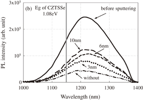
Fig. 4. (a) PL spectra after sputtering (dash lines) of the solar cells without and with CdS buffer layers of 3, 6, and 10 nm thicknesses and a PL spectrum before sputtering (solid line), (b) PL spectra after sputtering (dash lines) of the cells without and with (Cd,Zn)S buffer layers of 3, 6, and 10 nm thicknesses and a PL spectrum before sputtering (solid line). The 1.08 eV line is the Eg calculated from EQE.
Download figure:
Standard image High-resolution imageThe PL peak intensities after sputtering are lower than those before sputtering. The PL peak intensities after sputtering moreover decreased with decreasing CdS and (Cd,Zn)S thicknesses, where the PL peak intensities after sputtering of (Cd,Zn)S are lower than those of CdS of the same thickness. From the results, the non-radiative recombination centers (sputtering damage) near the CZTSSe surface could be estimated from the PL peak intensities after sputtering. In addition, they increase in density with decreasing in CdS and (Cd,Zn)S thicknesses, where the CdS buffer demonstrates better capability of preventing sputtering damage near the CZTSSe surface than the (Cd,Zn)S buffer. This is the reason why the photovoltaic performance of the solar cell with the CdS buffer is higher than that with the (Cd,Zn)S buffer, as shown in Table I and Fig. 2.
Figure 5 shows PL ratio as a function of buffer layer thickness. The PL ratio is here defined as the ratio of the PL peak intensity after sputtering to that before sputtering. In the figure, it is seen that the PL ratio of the cell without the buffer layer is below 0.2. The PL ratio also tends to increase with increasing thicknesses of both CdS and (Cd,Zn)S buffer layers, where the ratios for CdS are higher than those for (Cd,Zn)S at the same thickness. This clearly confirms that the CdS buffer shows a higher capability of preventing the sputtering damage on the CZTSSe surface than the (Cd,Zn)S buffer, leading to a higher cell performance for the former buffer. On the basis of the results, the PL ratio could be used as a practical indicator of sputtering damage.

Fig. 5. PL ratio as a function of buffer thickness of the CZTSSe solar cells without buffer (closed triangle) and with CdS (closed circles) and (Cd,Zn)S (open circles) buffer layers.
Download figure:
Standard image High-resolution imageFigure 6 shows the solar cell performance characteristics [JSC, open-circuit voltage (VOC), fill factor (FF), and the conversion efficiency (η)] as a function of PL ratio for determining sputtering damage. It is shown that VOC and FF are hardly affected by the PL ratio. On the other hand, JSC considerably increases with increasing PL ratio up to 0.5, followed by saturation at ratios higher than 0.5, thus leading to the improvement of η to approximately 8% at a ratio of 0.5 and a slight increase to about 10%, as depicted in Fig. 6(d).

Fig. 6. Solar cell parameters as a function of PL ratio. The closed triangles, closed circles, and open circles indicate the parameters of the solar cells without and with CdS and (Cd,Zn)S buffer layers, respectively.
Download figure:
Standard image High-resolution image
With the increase in the PL ratio up to 0.5, JSC and η improve, which is attributable to the reduction in sputtering damage on absorbers owing to the thicker buffer layer. In contrast, with the further increase in the PL ratio to higher than 0.5, namely, a greater increase in buffer layer thickness, the sputtering damage on the absorber surface decreases; however, these thicker buffer layers increase light absorption at shorter wavelengths (<520 nm). This leads to the slight increases in JSC and η in this PL ratio range. It is subsequently suggested that the high photovoltaic performance is achieved at a PL ratio of 0.5 or higher. This critical PL ratio of 0.5 is obtained when the CdS and (Cd,Zn)S buffer thicknesses are approximately 6 and 20 nm, respectively. The results obviously demonstrate that the PL ratio is a useful tool for evaluating the sputtering damage on the absorber surface to design the buffer layer (material and thickness) for the improvement of cell performance.
4. Conclusions
The CZTSSe solar cells were fabricated with CdS and (Cd,Zn)S buffer layers. It is found that the density of non-radiative recombination centers (sputtering damage) on the CZTSSe surface, investigated on the basis of PL peak intensity, decreases with increasing thicknesses of both CdS and (Cd,Zn)S buffer layers. In addition, the PL peak intensities after sputtering of the CdS buffer are higher than those of the (Cd,Zn)S buffer, suggesting that the CdS buffer layer demonstrates a better capability of preventing the sputtering damage on the CZTSSe surface than the (Cd,Zn)S buffer layer. Finally, the CZTSSe solar cells with η of approximately 10% are obtained when the PL ratio is 0.5 or higher. This PL ratio is proved to be a practical tool for investigating the sputtering damage on the absorber surface for the development of the CZTSSe solar cell.
Acknowledgments
This work was partly conducted within the research consortium of "Development of high-efficiency CZTS solar cells and submodules" in the Research and Development of Solar Energy Technology Project of the New Energy and Industrial Technology Development Organization (NEDO) of Japan. We acknowledge the Research Center for Photovoltaic Technologies, Advanced Industrial Science and Technology (AIST), for advice on solar cell fabrication.