Abstract
Many important processes take place at solid/liquid interfaces. To understand these processes, in situ real-time evaluation of the geometric, electronic, and molecular structures at solid/liquid interfaces at the atomic and molecular levels is essential. Owing to the presence of the liquid, however, techniques such as electron microscopy and low-energy electron diffraction, which are powerful tools for surface structural analysis in vacuum, cannot be used for solid/liquid interfaces. In this review, various techniques applicable to solid/liquid interfaces, including scanning probe microscopy, synchrotron-radiation-based X-ray techniques, and nonlinear spectroscopy, are briefly described. The characterization of the electrodeposition process of Pd layers on Au single-crystal electrode surfaces is presented as an example to demonstrate the importance of using multiple techniques in an integrated manner to understand the processes at solid/liquid interfaces.
Export citation and abstract BibTeX RIS
1. Introduction
Many important processes, including crystal growth, corrosion, electrode reactions, and biological processes, take place at solid/liquid interfaces. To understand these processes in detail, it is essential to clarify the geometric and electronic structures of interfaces as well as the molecular structure and orientation of reactants, products, intermediates, and solvent at the interface with atomic and molecular resolution in situ in real time. However, techniques such as electron microscopy, low-energy electron diffraction (LEED), and X-ray photoelectron spectroscopy (XPS), which are powerful tools for analyzing the surface structure and electronic state in vacuum utilizing electrons as a probe, cannot be applied to solid/liquid interfaces because of the presence of the liquid. Thanks to the significant research efforts during the last 25 years, many techniques that can be applicable to solid/liquid interfaces, such as scanning probe microscopy (SPM), nonlinear spectroscopy, and synchrotron-radiation-based X-ray techniques, as shown in Table I, have been developed and experiments using clean single-crystal surfaces in solution have become possible. As a result, the in situ real-time monitoring of structures at solid/liquid interfaces has become possible and the understanding of the reactions and processes at solid/liquid interfaces has considerably progressed.1) In the following sections, the application of the techniques summarized in Table I to study processes at solid/liquid interfaces, particularly electrochemical processes, are briefly described by showing mainly our results. The importance of using multiple techniques in an integrated manner to understand the processes at solid/liquid interfaces is also demonstrated by presenting an example.
Table I. Typical techniques used for in situ evaluation of solid/liquid interfaces.
| Technique | Object | Note | |
|---|---|---|---|
| Scanning tunneling microscopy | STM | Surface local (electronic) structure | Outermost layer of conductor only |
| Atomic force microscopy | AFM | Surface local structure | Applicable to insulator but outermost layer only |
| Surface X-ray scattering | SXS | Interfacial structure | Very high resolution, long range order required |
| X-ray absorption fine structure | XAFS | Local structure, oxidation number, coordination number | Restriction for substrate-surface species combination |
| Second harmonic generation | SHG | Symmetry and electronic structure of surface | Complicated analysis |
| X-ray photoelectron spectroscopy | XPS | Electronic structure | Vacuum required → New system for in situ operation is under development |
| IR reflection absorption spectroscopy | IRRAS | Identification and structure of molecules at interface | IR absorption by water |
| Sum frequency generation spectroscopy | SFG | Identification and structure of molecules at interface | IR absorption by water, complicated analysis |
| Surface enhanced Raman scattering | SERS | Identification and structure of molecules at interface | Limited objects |
| Ellipsometry | Thickness and optical properties of interfacial layer | ||
| Quartz crystal microbalance | QCM | Interfacial mass | Effect of viscosity |
2. Geometric structure
Reactions at solid surfaces are strongly dependent on geometric structures such as the orientation and atomic arrangement of the substrates. Although the geometric structure (atomic arrangement) of a solid surface with long-range order can be determined by LEED in vacuum, LEED cannot be used in solution since electrons significantly interact with matter. Scanning probe microscopies, i.e., scanning tunneling microscopy (STM) and atomic force microscopy (AFM), and X-ray techniques are applicable to solid/liquid interfaces.
2.1. STM
Using STM, which was developed by Binning and Rohrer of IBM Zurich Research Laboratory in 1982, atomic images of solid surfaces can be obtained in not only ultrahigh vacuum but also an ambient atmosphere, insulating liquids, and even electrolyte solutions, and its effectiveness in the field of electrochemistry has been demonstrated. Since there have already been many reviews on the principle of STM,2) here I concentrate on describing the application of STM to solid/liquid, particularly electrochemical, interfaces.
In ordinary STM measurements, a bias is applied between the very closely placed sample and tip, and the tunneling current flowing between them is used as a probe. When the tip is scanned over the sample surface, the tunneling current changes with the distance between the sample and the tip, reflecting the surface topography, and the surface structure can be imaged. However, this method cannot be applied to electrochemical systems without modification. Placing only a sample and a tip in a solution and applying a bias between them is equivalent to carrying out electrochemical reactions in a two-electrode configuration, in which the electrode potential of the sample cannot be controlled as there is no reference electrode and, therefore, it is not possible to examine a specific reaction by this method. Furthermore, a current equal to that flowing at the sample surface due to an electrochemical reaction (Faradaic current) flows at the tip because the tip serves as a counter electrode (CE), and since the Faradaic current is generally much larger than the tunneling current, STM measurement is impossible in this configuration. In addition, the tip surface may change as a result of electrochemical reactions at the tip surface. Therefore, for electrochemical STM measurement, a reference electrode (RE) and a CE in addition to the sample and the tip should be placed in an electrochemical cell [Fig. 1(a)] so that the potential applied to the sample [working electrode (WE)] and the tip can be individually controlled with respect to the RE and the desired electrochemical reaction at the sample can be induced while preventing an electrochemical reaction at the tip.3) In this case, the Faradaic current flows only between the sample and the CE, and only tunneling current flows between the sample and the tip. A material that is stable in the solution should be used as the tip material. It is also important to suppress the current at the tip by covering the tip surface, except for the very end of the tip, with insulating resin or glass to minimize the area of the tip exposed to the solution.

Download figure:
Standard image High-resolution image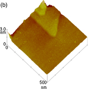
Download figure:
Standard image High-resolution image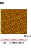
Download figure:
Standard image High-resolution image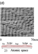
Fig. 1. (a) Schematic of electrochemical STM cell. (b–d) STM images of a Au(111) surface in a 50 mM sulfuric acid solution obtained under potential control. (b) 500 × 500 nm2 image obtained at +0.95 V, (c) 10 × 10 nm2 image obtained at +0.95 V, and (d) 70 × 70 nm2 image obtained at −0.2 V.
Download figure:
Standard image High-resolution imageFigures 1(b)–1(d) show STM images of Au(111) surfaces in sulfuric acid solution obtained under potential control. A large atomically flat terrace and steps of monatomic height that intersect at an angle of 60° are observed in a 500 × 500 nm2 image obtained at 0.95 V [Fig. 1(b)]. In the magnified image of 10 × 10 nm2, individual Au atoms, which are arranged hexagonally with a distance of approximately 0.29 nm, corresponding to a 1 × 1 structure, are observed [Fig. 1(c)].4) At −0.2 V, a herringbone structure, indicating the reconstruction of surface atoms into a  structure, is observed [Fig. 1(d)].5)
2.2. AFM
STM measurements cannot be performed for insulators and even metals when an insulating layer such as an oxide layer is formed on their surface, because STM uses the tunneling current between the tip and the sample as a probe. The potential range for the observation of a semiconductor electrode surface is also limited because of the existence of a space-charge layer in the reverse bias region. In contrast, AFM, which uses the atomic force between the tip and the sample, has a high spatial resolution similar to that of STM but is not restricted by the conductivity of the sample surface.6) Moreover, AFM has an advantage over STM as electrochemical reactions at the tip surface do not affect the measurement. AFM has been used to monitor the reactions at semiconductor electrode surfaces and the deposition of insulating materials since the early 1990s.7) Recently, the importance of AFM as a technique to determine the structure at solid/liquid interfaces including soft interfaces has increased with the development of non-contact AFM with high lateral resolution.8)
2.3. Synchrotron-radiation-based X-ray techniques
Although the structure of a solid surface can be determined with high resolution by STM and AFM, the information is limited to that of the outermost layer and three-dimensional structural information cannot be obtained. In addition, the lateral resolution is low. X-rays are an excellent probe light that can be used for structural analysis with atomic/molecular resolution because the wavelength of X-rays (0.01–10 Å) is equivalent to the size of atoms and ions. In addition, X-rays are considered to be ideal for the structural analysis of solid/liquid interfaces because they transmit through water without significant absorption. However, it is impossible to retrieve information on the electrode surface (or electrode/solution interface) selectively with a high signal-to-noise (S/N) ratio using X-ray sources in laboratories owing to their low intensity and directionality. Therefore, the application of X-ray techniques to electrochemical interfaces using such X-rays is limited to the study of material layers with a certain thickness. Because synchrotron radiation has high brilliance and directionality and a continuous wavelength distribution, it has brought about a revolutionary change in the use of X-rays in the field of surface science. Synchrotron-radiation-based X-ray techniques have been applied for the in situ structural evaluation of electrode/solution interfaces since around 1980.9,10)
2.3.1. Surface X-ray scattering
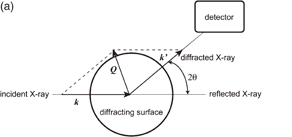
Surface X-ray scattering (SXS) techniques include surface X-ray diffraction (SXRD) and crystal truncation rod (CTR) analysis. In ordinary X-ray diffraction measurements, the incident angle of X-rays is higher than the critical angle at which total reflection starts to occur, and the bulk structure of three-dimensional crystals is determined by analyzing the intensity distribution of the diffracted light as a function of the angle of diffraction. On the other hand, in SXRD techniques, the incident angle of X-rays is less than 2–3 mrad, i.e., less than the critical angle, so that information on the surface can be selectively obtained. In this case, the X-rays penetrate only 1–10 nm into the sample and most of the X-rays are specularly reflected. However, when a two-dimensionally ordered structure is present at the sample surface, a small portion of the X-rays (that penetrate into the sample) are laterally diffracted by the surface structure (Fig. 2). In Fig. 2, k and k' are the incident and diffracted X-ray vectors, respectively, and Q is the scattering vector, which is given by Q = k' − k and is divided into a lateral component (Q∥) and a vertical component (Q⊥). 2θ is the angle of diffraction, ϕ is the azimuth of the sample surface, χ is the angle between the sample surface and Q, and α and β are the angles between the sample surface and k and k', respectively. In actual SXRD measurement, the intensity of diffracted light is measured when Q∥ is varied by changing the position of the detector (2θ) or by rotating the sample (changing ϕ) at a very small Q⊥ (β or χ). When Q∥ becomes equal to one of the reciprocal lattice vectors of the laterally ordered structure of the electrode surface, a diffraction peak is observed. The spacing of atomic rows, d, is determined from the value of Q∥ that corresponds to the peak. In addition, the orientation of the structure with an atomic spacing of d can be determined by rotating only the sample (changing ϕ) while keeping the detector at 2θ (constant Q∥, i.e., constant d). Thus, the two-dimensional structure of the electrode surface can be determined from the dependence of the intensity of diffracted light on Q∥ and ϕ.
Download figure:
Standard image High-resolution image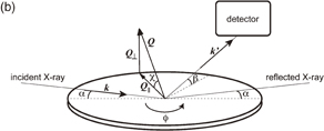
Fig. 2. Schematic of SXS showing X-ray vectors viewed from (a) directly above and (b) obliquely above the sample.
Download figure:
Standard image High-resolution imageWhen the lateral position of the detector is fixed (constant 2θ) and the detector is scanned only in the vertical direction (changing χ, i.e., Q⊥), a diffraction pattern called a CTR is obtained. While diffraction is observed only at Bragg positions in the ordinary XRD measurement for a bulk structure, diffraction is observed even between Bragg positions, reflecting the structure of the surface (interface), in the case of SXRD, and, therefore, the structure of the electrode in the vicinity of the surface in the vertical direction can be determined by CTR analysis. Since SXRD and CTR measurements can be carried out in the same experimental configuration, the structure of solid/liquid interfaces is generally determined by comprehensively analyzing the results of both measurements.
Figure 3(a) shows a schematic of an electrochemical cell used for SXS measurement.11) To minimize the scattering of X-rays by the solution and window, SXS measurements are carried out while maintaining a solution layer thin (a few µm) using an ultrathin polymer layer (thickness: a few µm) with high X-ray transmittance as a window. Since a too thin solution layer results in a nonuniform potential distribution, SXS measurements are generally carried out after the ultrathin polymer layer has been expanded to increase the solution layer thickness, a certain potential is applied to the electrode surface for a predetermined duration so that the electrochemical reaction proceeds uniformly, and then the thickness of the solution layer is decreased to stop further reaction. Figures 3(b) and 3(c) show the potential-dependent structural changes of a Au(111) electrode. Figure 3(b) shows SXRD patterns obtained by measuring the diffraction intensity along the vector (qr) in the reciprocal lattice plane shown in the inset,12) where the origin is the position of the diffraction peak corresponding to the 1 × 1 structure and the direction relative to the diffraction peak corresponding to the  structure is defined as qr. In the negative-potential region, in addition to a peak corresponding to the 1 × 1 structure at qr = 0, a peak corresponding to the
  reconstructed structure is observed at qr = 0.038 [Fig. 3(b) (A)]. In contrast, in the positive-potential region, the peak corresponding to the reconstructed structure disappears and the height of the peak corresponding to the 1 × 1 structure significantly increases [Fig. 3(b) (B)]. These results support the STM observation of the potential-dependent appearance and disappearance of the reconstructed structure shown in Fig. 1. More detailed information onthe potential-dependent three-dimensional structure at the Au(111)/H2SO4 solution interface can be obtained by combining the above results with those of CTR measurement [Fig. 3(c)].11) When the potential is made positive, the reconstructed structure present in the negative-potential region [Fig. 3(b) (A)] is lifted, sulfate anions are adsorbed on the 1 × 1 surface [Fig. 3(b) (A) and Fig. 3(c) (B)], oxygen species (hydroxide ions) are adsorbed on the 1 × 1 surface, and oxygen atoms penetrate into the Pt layer [Fig. 3(c) (C)]. When the potential is made negative again, the reverse processes take place almost reversibly but the surface at the original potential is slightly rougher than the initial structure and the formation of oxides and their reduction are not completely reversible when potential cycles are repeated. Thus, the potential-dependent three-dimensional structure of electrode/electrolyte interfaces can be clarified in detail by combining STM and SXS measurements.
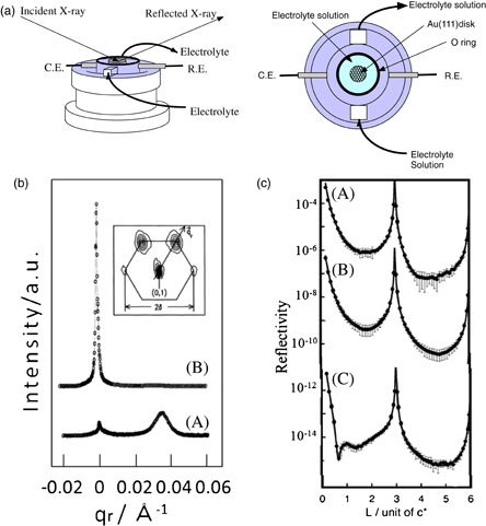
Fig. 3. (a) Electrochemical cell used for SXS measurement. (b) SXRD patterns of Au(111) electrode at (A) negative potential and (B) positive potential. (c) CTR at (A) 0 V, (B) +0.95 V, and (C) +1.40 V.
Download figure:
Standard image High-resolution image2.3.2. X-ray absorption fine structure
Since SXS is only applicable to crystalline solid surfaces because it utilizes the diffraction induced by structures with long-range order, for local structures of materials without long-range order, i.e., non-crystalline materials, X-ray absorption fine structure (XAFS) is used. X-ray absorption spectra are generally obtained by measuring the absorption of light by the sample, μt (μ, absorption coefficient; t, thickness of the sample), as a function of the incident light energy, as is the case in ultraviolet and visible absorption spectra measurement. Figure 4(a) shows a typical X-ray absorption spectrum. It is clear that the absorption of the X-rays markedly increases at the absorption edge, where the incident X-ray energy becomes equal to the binding energy, which is determined by the absorbing atom, the quantum numbers of inner-shell electrons to be excited, and the electronic configuration of the valence band. The absorption edge energy is expressed by the symbols for an element and electron shell. The spectrum in Fig. 4(a) is the X-ray absorption spectrum of the Pt-L3 edge. The absorption gradually decreases with increasing incident X-ray energy above the absorption edge, but at the same time a fine structure (oscillating structure) is observed over an energy of approximately 1000 eV above the absorption edge. The XAFS includes the X-ray absorption near-edge structure (XANES), which is observed approximately ±50 eV from the absorption edge, and the extended X-ray absorption fine structure (EXAFS), which is observed at higher energies. Many books and reviews are available on the analysis of the XAFS.13) Briefly, the XANES reflects the structure of an unoccupied orbital or band, and XANES analysis provides information on the orientation (symmetry) of unoccupied orbitals and the electron configuration (oxidation state). In contrast, EXAFS oscillation is caused by the interference between the emitted electrons as a result of X-ray absorption (traveling waves) and the electron waves backscattered by neighboring atoms, as shown in the inset of Fig. 4(a). Therefore, analysis of the EXAFS oscillation reveals the local structures including neighboring atomic species and their coordination number. The XAFS spectra of liquids and powders are generally obtained by measuring the intensity of X-rays before and after transmission through the sample as a function of X-ray energy (transmission mode). This method, however, cannot be applied to solid/liquid interfaces. Instead, spectra are obtained by measuring the intensity of fluorescent X-rays generated by X-ray absorption as a function of X-ray energy typically using a solid-state detector (SSD). In this case, information on structural anisotropy can also be obtained by measuring the polarization dependence. Figure 4(b) shows a typical electrochemical XAFS measurement system. The electrochemical cell used in SXS measurement can also be used for XAFS measurement.14) Figure 5(a) shows the EXAFS function χ(k) multiplied by the weighting factor k2 (k is the wavenumber of incident light) of K2PtCl42− solution and PtCl42− introduced into a viologen molecular layer formed on a Si(111) surface by ion exchange under various conditions. Here, χ(k) is obtained by subtracting the background (Δμt) from the XAFS spectrum, and the multiplication by the weighting factor k2 is carried out because χ(k) is the sum of the contributions by multiple scattering atoms.15) Figure 5(b) shows the model structures based on a FEFF simulation16) for the EXAFS region and the analysis of the XANES region. It is shown that Pt complexes, in which ligands (chloride ions) are replaced by oxygen species, serve as a catalyst for hydrogen evolution. The Fourier transform indicates that no Pt–Pt bonds are present, supporting the above results.

Download figure:
Standard image High-resolution image
Fig. 4. (a) Typical X-ray absorption spectrum (Pt-L3 absorption). Inset: Schematic of EXAFS oscillation. (b) Electrochemical XAFS measurement system.
Download figure:
Standard image High-resolution image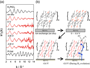
Fig. 5. (a) k dependence of k2-weighted EXAFS oscillation x(k) of PtCl42−, which was incorporated by ion exchange into a viologen molecular layer with an electron transfer function formed on a Si(111) surface, under various conditions, (b) model structures based on FEFF simulation for the EXAFS region and analysis of the XANES region.
Download figure:
Standard image High-resolution image3. Electronic structure
The reactivity of solid surfaces is significantly affected by not only the geometric structure but also the electronic structure of the surface. Photoelectron spectroscopy, a powerful tool for obtaining information on the electronic structure in vacuum, cannot be used in solution17) but techniques using light as a probe can be effectively applied for the analysis of solid/liquid interfaces.
3.1. XANES
As described above, XANES enables in situ monitoring of the oxidation state of a central atom at solid/liquid interfaces using X-rays as a probe. Figure 6 shows the results of XANES measurements, which were carried out to clarify the origin of the electrocatalytic activity enhancement of Pt for the oxygen reduction reaction (ORR) upon the addition of a CeO2 co-catalyst.18) Figures 6(a) and 6(b) show the XANES spectra of Pt and Ce, respectively. While the oxidation state of Pt can be evaluated from the intensity of the white line (the peak in the vicinity of the absorption edge), the shape of the XANES spectra of Ce strongly depends on the oxidation state of Ce. While two peaks corresponding to Ce4+ are observed in the spectrum of CeO2 [Fig. 6(b) (A)], an additional peak corresponding to Ce3+ is observed on the lower-energy side in the spectrum of carbon-supported Pt–CeOx [Fig. 6(b) (B)]. In the XANES spectrum obtained after Pt–CeOx is immersed in a sulfuric acid solution [Fig. 6(b) (C)], the two peaks corresponding to Ce4+ are hardly visible and only the peak corresponding to Ce3+ is observed. Figures 6(c) and 6(d) show the potential dependences of the white-line intensity of Pt in an ordinary carbon-supported Pt catalyst, and the white-line intensity of Pt and the intensities of Ce3+ and Ce4+ in carbon-supported Pt–CeOx, respectively. In the case of the ordinary Pt catalyst, Pt oxide is formed partially on the Pt surface at potentials where the ORR takes place. In contrast, in the case of the Pt–CeOx nanocomposite, Pt oxide formation is significantly suppressed and the amount of the Ce3+ component decreases and the amount of the Ce4+ component increases as the potential becomes more positive. These results indicate that the Ce3+ component in CeOx is oxidized instead of Pt because of charge transfer at the Pt/CeOx interface, resulting in the suppression of Pt oxidation. Since the catalytic activity of Pt for the ORR is known to decrease upon the formation of surface Pt oxide, it can be concluded that the Pt–CeOx nanocomposite shows higher electrocatalytic activity for the ORR because the intrinsic catalytic activity of Pt is expressed owing to the suppression of Pt oxide formation by CeOx.
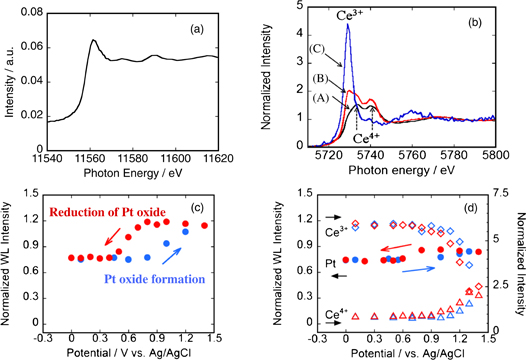
Fig. 6. (a) XANES spectrum of Pt–CeO2 at the Pt L3 edge. (b) Normalized XANES spectra at the Ce L3 edge of (A) pure CeO2, (B) C-supported Pt–CeOx, and (C) C-supported Pt–CeOx after immersion in 0.5 M H2SO4 solution for 30 min. Potential dependences of (c) normalized WL intensity of Pt in C-supported Pt catalyst, and (d) WL intensity of Pt and intensities in Ce3+ and Ce4+ of C-supported Pt–CeOx.
Download figure:
Standard image High-resolution image3.2. Second harmonic generation spectroscopy
When intense light is focused on a solid surface, light with twice the energy of the incident light is generated. This is one of the second-order nonlinear optical phenomena called second harmonic generation (SHG).19) SHG is not observed in isotropic media such as gas and liquid phases and is only observed at surfaces and interfaces where the inversion symmetry is broken. In addition, the SHG signal is resonantly enhanced when the energy of the incident light or second harmonic light (or both) becomes equal to the transition energy between energy states at the interface [Fig. 7(a), insets (i)–(iii)]. Therefore, the electronic spectrum at the interface can be obtained by measuring the SHG intensity as a function of the energy of the incident light. Figure 7(b) shows a schematic of a spectroelectrochemical cell used for electrochemical SHG measurement. By allowing only the surface of a specific index of a single-crystal electrode comes into contact with an electrolyte solution, both the electrochemical response and the SHG characteristics at the surface of the specific index are obtained. The laser light used for SHG measurement is gently focused on the electrode surface from the electrolyte solution (bottom) side after passing through a polarizer and a filter. Second harmonic (SH) light that is emitted almost coaxially with the reflected light is extracted using a filter and a monochromator then detected using a photomultiplier tube (PMT). Since both the incident light and the SH light are in the UV/visible region, absorption by the solution is generally not a problem. Figure 7(a) shows the wavelength dependence of the SHG enhancement factor associated with CO adsorption on a Pt electrode surface. This result suggests that the spectrum corresponds to the electronic transition from the Fermi level of Pt to an antibonding orbital of the adsorbed CO (2π*) [Fig. 7(a), insets].20) The anisotropy of the surface electronic structure can be determined by measuring the SHG intensity while rotating the sample,19) which is demonstrated to be effective for determining the surface chirality.21)

Download figure:
Standard image High-resolution image
Fig. 7. (a) Wavelength dependence of SHG enhancement factor associated with CO adsorption on Pt electrode surface. Insets (i)–(iii), principle of SHG; (iv) schematic energy diagram of Pt electrode with adsorbed CO. (b) Spectroelectrochemical cell used for electrochemical SHG spectroscopy.
Download figure:
Standard image High-resolution image4. Molecular structure
Information of not only the surface structure of a solid itself but also the structure of chemical species at the interface such as reactants, intermediates, products, the solvent, and reaction inhibitors is necessary to understand the reactions at solid/liquid interfaces. Vibrational spectroscopy is the most effective method to obtain such information.
4.1. Infrared reflection absorption spectroscopy
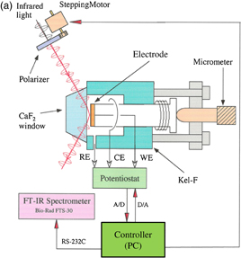
Although one of the most powerful tools for determining molecular structures is infrared (IR) spectroscopy, it was not successfully applied to study solid/liquid interfaces, because (1) it is difficult to separate the signal due to the molecular species at the solid/liquid interface from that due to molecules existing in abundance in the solution and (2) solvents, particularly water, strongly absorb IR light, until the pioneering work of Bewick et al. in the early 1980s opened a new era in the application of IR spectroscopy to electrochemical interfaces.10,22,23) They developed electrochemically modulated IR spectroscopy (EMIRS), in which the difference spectra between two modulating potentials reflecting the differences in the structure and the amount of adsorbates at these two potentials are obtained, thus greatly improving the sensitivity.23) They also minimized the interference due to IR absorption by water by pressing the electrode against an optical window to keep the thickness of the solution layer at 2–3 µm. EMIRS is a very simple method with high sensitivity and is suitable for obtaining the spectra of surface adsorbates separately from the strong IR absorption due to molecules in the solution bulk and a solvent such as water. However, EMIRS can be used only when the structure and the amount of the target adsorbed species change reversibly with the potential.
While s-polarized light that is perpendicular to the incident/reflection plane is not absorbed by surface molecules because its phase is shifted by 180° and the electric field vector is zero at the surface, p-polarized light that is parallel to the incident/reflection plane is absorbed by surface molecules because a strong electric field perpendicular to the surface is formed by the interference between the incident light and reflected light. Thus, information on the surface molecules is contained only in the p-polarized component. At a metal surface the maximum sensitivity is obtained when the incident angle of IR light is 80–85° and stretching vibration perpendicular to the surface is selectively observed because the direction of the electric field that excites the adsorbed molecules is perpendicular to the metal surface. The orientation angle of adsorbates can be determined on the basis of this surface selection rule. Furthermore, the reflection absorption spectrum of surface molecular species can be obtained by rapidly switching the incident light between p- and s-polarization under a constant potential [polarization modulation IR reflection absorption spectroscopy (PM-IRRAS)] using the following equation:

Here, Ip and Is are the intensities of p- and s-polarized light, respectively. PM-IRRAS does not require a reference substrate and the background can be removed easily. However, the sensitivity of PM-IRRAS in electrochemical systems is often insufficient and, therefore, subtractively normalized interfacial Fourier transform IR spectroscopy (SNIFTIRS) is more generally used in electrochemical systems. In SNIFTRS, spectra (interferograms) at the reference and measurement potentials are measured and integrated interchangeably, and the difference between the spectra at these two potentials is obtained. By doing so, the effects of the drift of the light source and other factors can be minimized, enabling spectra to be obtained with high sensitivity. One must note that the obtained result is a difference spectrum.
Figure 8(a) shows a typical spectroelectrochemical cell used for IRRAS. It has a CaF2 window and the distance between the electrode and the CaF2 window, i.e., the thickness of the solution layer, can be finely controlled by a micrometer. Figure 8(b) shows the spectra of a self-assembled monolayer of ferrocenethiol on a Au surface at various potentials using p-polarized light with the spectrum at 100 mV as a reference. The following electrochemical reaction is known to occur at the terminal ferrocene (Fc) moieties:

In the spectra observed at potentials of more positive than 650 mV, where the oxidation of Fc moieties takes place, downward peaks corresponding to an increase in absorption, such as the CH stretching vibration of the ferrocene ring, and upward peaks corresponding to a decrease in absorption, such as the CH stretching vibration of the methylene group of the alkyl chain, are observed, indicating that the molecular axis becomes more perpendicular to the Au surface [Fig. 8(c)]. These peaks are not observed in the spectra obtained with s-polarized light. When the potential is made more positive to +1.5 V, downward peaks corresponding to the CO stretching of CO2 and the SO stretching of SO2 are observed not only in the spectra obtained with p-polarized light but also in the spectra obtained with s-polarized light, showing that these chemical species exist in the solution. These findings indicate that Au–S bonds are broken by anodic oxidation, the molecules are dissolved in the solution, and some of them are oxidized to CO2.24)
Download figure:
Standard image High-resolution image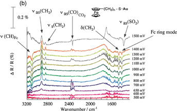
Download figure:
Standard image High-resolution image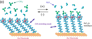
Download figure:
Standard image High-resolution image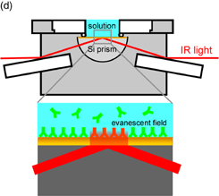
Fig. 8. (a) Spectroelectrochemical cell used for IRRAS. (b) Spectra of self-assembled monolayer of ferrocenethiol on a Au surface at various potentials using the spectrum at 100 mV as a reference (p-polarization). (c) Model. (d) ATR-IR (SEIRA) cell.
Download figure:
Standard image High-resolution imageThis technique suffers from the problems of the large solution resistance, a large time constant for the application of potential, nonuniform distribution of the potential, and suppressed diffusion of the reactants and products because of the low solution thickness of 2–3 µm, which is required to minimize the IR absorption by the solution. To avoid these problems, internal-reflection-type attenuated total reflection IR (ATR-IR) spectroscopy is often used. In ATR-IR spectroscopy, a thin metal layer, which is vacuum deposited on a prism surface that is in contact with the electrolyte solution, is used as an electrode as shown in Fig. 8(d). Although most of the IR light incident from the prism side is reflected at the prism/metal/solution interface, some of the IR light penetrates 200–300 nm into the solution and interacts with the molecules at the interface. By controlling the surface roughness and thickness of the thin metal layer, the IR absorption by the adsorbed molecules is markedly enhanced, which is known as surface-enhanced IR absorption (SEIRA). This enhancement effect decreases rapidly with increasing distance from the metal surface up to 2–3 nm, enabling the observation of molecules at the interface with high sensitivity and selectivity.25) Although ATR-IR spectroscopy has various advantages such as the same surface selection rule as reflection absorption IR spectroscopy [Fig. 8(a)] is applied, the sensitivity is at least ten times higher than that of the conventional IRRAS, there is no limit to the solution layer thickness, and, therefore, high-speed measurement is possible, it also has several disadvantages. For example, only a few metals such as Au, Ag, and Cu exhibit the SEIRA effect, and single-crystal electrodes with a well-defined surface structure cannot be used. Therefore, the above two techniques should be complementarily used depending on the purpose.
4.2. Surface-enhanced Raman scattering
When a material is irradiated with visible light with a given frequency, ν0, scattered light with an energy smaller than that of the original light with a frequency of ν0 − ν due to inelastic scattering (Stokes light) is detected in addition to elastically scattered light with the original frequency (Rayleigh light) [Fig. 9(a)]. The energy shift of Stokes light (change in frequency, ν) corresponds to the molecular vibration or lattice vibration of crystals and is thus used for the structural analysis of molecular species. Although both Raman spectra and IR spectra provide essentially the same information on the molecular vibration, their surface selection rules are different and, therefore, they are complementary. Since both excitation light and detection light are in the visible light region and there is no need to use IR light as a probe light in Raman scattering, measurement with a thick solution layer configuration is possible, and, therefore, the Raman scattering technique is considered to be very effective for the measurement at solid/liquid interfaces. However, the cross section of Raman scattering is small and, therefore, it is difficult to obtain Raman spectra of surface species. The application of Raman scattering for surface vibrational spectroscopy started in the 1970s when it was found that the Raman intensity is significantly increased if a roughened silver surface is used as a substrate.26) This phenomenon is called surface-enhanced Raman scattering (SERS). However, as for SEIRA, only a very limited range of substrates can be used and single-crystal surfaces cannot be used for SERS. We found recently that the Raman intensity is significantly enhanced by a factor of approximately 106 by depositing gold nanoparticles on a molecular layer formed on a metal surface including a single-crystal surface and that this technique is also applicable to even non-SERS-active metal substrates. We named the spectroscopy based on this concept gap-mode Raman spectroscopy.27) Figure 9(b) shows Raman spectra of a 4-chlorophenyl isocyanide (CPI) monomolecular layer formed on Pt(100) and Au(100) surfaces. No peak is observed in the Raman spectrum of CPI adsorbed on a Pt(100) surface shown in Fig. 9(b) (A) as expected. However, once Au nanoparticles are adsorbed on the CPI monomolecular layer on the Pt(100) surface, peaks are clearly observed, as shown in Fig. 9(b) (B), demonstrating that a Raman spectrum is obtained with high sensitivity on a non-SERS-active Pt single-crystal surface. This spectrum is different from the gap-mode Raman spectrum of a CPI monomolecular layer on a Au(100) surface shown in Fig. 9(b) (C), including the peak position of the C–N stretching vibration. This result indicates that gap-mode Raman spectroscopy provides information on the substrate-dependent structure of adsorbed molecules.28) Although these spectra were obtained in air, potential-dependent spectra in electrochemical systems have also been obtained.29)
Download figure:
Standard image High-resolution image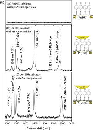
Fig. 9. (a) Principle of Raman scattering. (b) Raman spectra of (A) CPI molecular layer formed on Pt(100) surface without Au nanoparticles, (B) CPI molecular layer formed on Pt(100) surface with adsorbed Au nanoparticles, and (C) CPI molecular layer formed on Au(100) surface with adsorbed Au nanoparticles.
Download figure:
Standard image High-resolution image4.3. Sum frequency generation spectroscopy
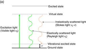
When two photons with different energies are incident, a photon with energy equal to the sum of the energies of the two input photons is generated. This phenomenon is called sum frequency generation (SFG) and is one of the second-order nonlinear optical phenomena such as SHG.30) SFG does not take place in centrosymmetric media and occurs only at interfaces where centrosymmetry is broken. Figure 10(a) shows the principle of SFG spectroscopy. If visible light with a fixed angular frequency of ωVIS and IR light with a variable angular frequency of ωIR are used as incident light and the angular frequency of the IR light becomes equal to that of the transition energy of the absorbed species (ωn) on the surface, the intensity of the SFG light (ωSFG) is resonantly enhanced. A surface (interfacial)-selective vibrational spectrum [Fig. 10(a), lower figure] is obtained by plotting the SFG intensity as a function of ωIR (note that the SFG light with intensity ωSFG is in the visible region). Molecules in a solution do not contribute to the SFG spectra and only information on the molecules at solid/liquid interfaces is obtained because the solution bulk is centrosymmetric. As is clear from the energy diagram in the upper part of Fig. 10(a), only transitions that are both IR- and Raman-active are SFG-active.

Download figure:
Standard image High-resolution image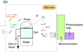
Download figure:
Standard image High-resolution image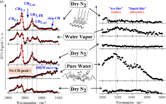
Fig. 10. (a) Principle of resonant enhancement of SFG intensity with SFG spectrum. (b) SFG measurement system for solid/liquid interface. (c) SFG spectra of CH (left) and OH (right) regions of alkylated poly(vinyl pyridine) brushes obtained in various environments.
Download figure:
Standard image High-resolution imageFigure 10(b) shows a schematic of the SFG measurement system used for solid/liquid interfaces. An internal-reflection mode with a prism is generally adopted to avoid the absorption of IR light by the solvent (particularly water). The IR and visible lights incident from the back side of the prism are totally reflected at the solution/prism interface, and the emitted sum frequency light is separated from the reflected light spatially and/or by using a filter and monochromator and then detected by a photomultiplier tube.
Figure 10(c) shows how the structure of alkylated poly(vinyl pyridine) brushes formed on a prism surface changes with the environment, as observed by SFG spectroscopy.31) The SFG spectra in the CH stretching region [Fig. 10(c), left figure] show that (1) the alkyl chain is almost in the all-trans conformation in dry nitrogen as the SFG intensity of the CH stretching of the methyl group is much stronger than that of the CH stretching of the methylene group, although the number of methylene groups is much larger than that of methyl groups, (2) the SFG intensity of the CH stretching of the methyl group and that of the methylene group decreases and increases, respectively, showing the introduction of gauche defects, upon contact with water vapor, (3) the original structure is recovered upon subsequent contact with dry nitrogen, (4) no CH stretching peaks are observed upon contact with liquid water, indicating the completely disordered conformational structure of the alkyl chain, and (5) it takes time for the brushes to return to their original conformational structure after they have been in contact with liquid water even if they are placed in dry nitrogen. The SFG spectra in the OH stretching region [Fig. 10(c), right figure] show that water with a similar structure to that obtained upon contact with pure water is present at the surface even when the brushes are in contact with water vapor. In addition, the SFG intensity is relatively high in the low-wavenumber region, indicating that a high fraction of interfacial water is highly hydrogen-bonded, which is observed when water is in contact with a hydrophobic surface.
Both external- and internal-reflection configurations can be used when SFG spectroscopy is applied to electrochemical systems. In the external-reflection configuration, the electrode should be pressed onto an optical window so that the thickness of the solution layer between them can be minimized (2–3 µm) and the absorption of IR light by water can be suppressed, similar to the case of IR spectroscopy as explained above. In the internal-reflection configuration, the SFG measurements are carried out using a thin metal layer (thickness, 20–30 nm), which is deposited on a window that is transparent to IR light (e.g., CaF2, Al2O3, etc.) by vacuum deposition or sputtering, as a WE.32) The advantages and disadvantages of these two configurations for IRRAS given in Sect. 4.1 also apply to SFG spectroscopy. Furthermore, in the case of the internal-reflection mode, the thin metal layer may be damaged and even peel off when the laser light is too strong.
5. Thickness and mass of interphase
In addition to information on the geometric, electronic, and molecular structures of an interface as explained above, that on the thickness and mass of the interphase is essential to understand the processes at solid/liquid interfaces.
5.1. Ellipsometry
When light incident on an interface is reflected, the changes in the amplitude and phase are different between p- and s-polarized light because the amplitude reflection coefficient of p-polarized light, rp (= Erp/Eip), is different from that of s-polarized light, rs (= Ers/Eis), where Eip and Eis are the electric-field vectors of p- and s-polarized incident light, respectively, and Erp and Ers are the electric-field vectors of p- and s-polarized reflected light, respectively. The experimentally obtained amplitude ratio, tan Ψ, and phase difference, Δ, between the p- and s-polarized light are correlated with the ratio of the amplitude reflection coefficient of p-polarized light to that of s-polarized light, as expressed by

When linearly polarized light, in which the amplitudes of p- and s-polarized light are the same and their phase difference is 0, is used as the incident light, the reflected light is elliptically polarized, and Eq. (3) is rewritten as

The amplitude reflection coefficient is determined by the interaction of light with a material and depends on the complex index of refraction and the layer thickness. Although two values, Ψ and Δ, are experimentally obtained in ellipsometry, it is not possible to analytically obtain the complex index of refraction or the layer thickness from the values of Ψ and Δ. On the other hand, it is possible to calculate Ψ and Δ from the complex index of refraction and the layer thickness. Therefore, the complex index of refraction and the layer thickness are determined by comparing the values of Ψ and Δ calculated for the complex index of refraction and the layer thickness based on an appropriate optical model with the experimentally determined values of Ψ and Δ. The spectra of Ψ and Δ can be obtained by spectroscopic ellipsometry, in which the measurements are carried out while changing the wavelength of the incident light. Since both the incident and reflected light are generally visible in ellipsometry, the measurements are rarely affected by the solvent, and, therefore, ellipsometry is easily applicable to the evaluation of solid/liquid interfaces. It has been used to monitor the growth of thin films and the corrosion process at solid/liquid interfaces for many years,33) but it is also possible to follow processes in real-time at the monolayer level34,35) such as potential-dependent changes in the optical properties and thickness of a self-assembled monolayer of ferrocenethiol induced by oxidation-reduction of the terminal ferrocene group (Fig. 8).34)
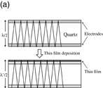
5.2. Quartz crystal microbalance
When an electric field is applied between two electrodes, which sandwich an AT-cut quartz crystal, standing waves with a resonant frequency determined by the thickness of the quartz crystal are generated. If a material is deposited (adsorbed) on the electrode surface, the thickness increases and the frequency of the standing wave decreases (Fig. 11).36) Assuming that the density and piezoelectric property of the material deposited (absorbed) on the surface of the quartz crystal are the same as those of the quartz, the relationship between the change in resonant frequency, Δf, and the change in mass, Δm, is expressed as

where f0 is the fundamental frequency, ρq and μq are the density and modulus of rigidity of the quartz, respectively, and A is the area exhibiting a piezoelectric response. The minus sign in Eq. (5) means that the frequency decreases with increasing mass. For example, at a resonant frequency of 5 MHz, a change in frequency of 1 Hz corresponds to a change in mass of ca. 17 ng/cm2. Since the change in surface mass can be measured with a very high sensitivity at a monatomic layer or monolayer level, this technique is called a quartz crystal microbalance (QCM) (or nanobalance). When a QCM is used to investigate solid/liquid interfaces, one of the electrodes is made to be in contact with the solution. When a QCM is applied to electrochemical systems, the electrode in contact with the solution is used as the WE, the potential of which is controlled by using a potentiostat. Figure 11(c) shows the simultaneously recorded current and Δf (resonant frequency, 5 MHz) as a function of potential at a Au electrode modified by a self-assembled monolayer of ferrocenethiol measured in a 1 M HClO4 solution while the potential was scanned at 20 mV/s. The changes in the surface mass during the oxidation-reduction cycle (Fig. 8) of the terminal ferrocene moieties of the self-assembled ferrocenethiol monolayer are detected. The charge, which is obtained by integrating the current during the oxidation-reduction cycle with respect to time, is linearly related to Δf (or Δm). From the slope of this linear relation, the surface mass change is calculated to be 100 g/F, which is equivalent to the molecular weight of perchlorate ion, confirming that the change in mass is associated with ion pair formation between the ferrocenium cation generated by the oxidation of the terminal ferrocene moiety and the perchlorate anion at the surface.37)
Download figure:
Standard image High-resolution image
Download figure:
Standard image High-resolution image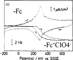
Fig. 11. (a) Model for the relation between the thickness of a quartz crystal, the resonant frequency, and the decrease in frequency caused by the deposition/adsorption of a material on the electrode surface. (b) Example of an electrochemical QCM measurement. (c) Potential dependences of simultaneously recorded current and Δf (resonant frequency, 5 MHz) at a Au electrode modified by a self-assembled monolayer of ferrocenethiol in a 1 M HClO4 solution while the potential was scanned at 20 mV/s.
Download figure:
Standard image High-resolution image6. Example of comprehensive analysis of processes at solid/liquid interfaces: Monitoring of electrodeposition process and structural evaluation of thin Pd layer on Au single-crystal electrode
In this section, the effectiveness of using multiple techniques in an integrated manner for analyzing interfacial processes is demonstrated by the monitoring of the electrochemical deposition of a thin Pd layer on a Au(111) single-crystal electrode surface to form metal electrodes with high catalytic activity as an example.
Figure 12(a) (A) shows a 10 × 10 nm2 STM image of a Au(111) surface in a 0.5 M H2SO4 solution containing 0.1 mM of a Pd complex (PdCl42−) obtained at 0.95 V, which is more positive than the Pd deposition potential. This is completely different from the STM image of the Au(111) surface obtained in a sulfuric acid solution without the Pd complex shown in Fig. 1(c). Hexagonally arranged spots with a nearest-neighbor distance of approximately 0.78 nm [ times that of the Au(111) lattice] are observed, indicating the adsorption of some species from the solution. The symmetry of the adlattice is rotated by ca. 20° relative to that of the Au(111) substrate, suggesting that the adlayer structure is (
 ) R19.1°. When QCM measurement is carried out at the Au electrode in a 0.5 M H2SO4 solution while keeping the potential at 0.95 V and adding K2PdCl4 solution to make a final concentration of 0.1 mM while gently stirring the solution, the surface mass is increased by ca. 87 ng/cm2, suggesting the adsorption of PdCl42−. The number of adsorbed PdCl42− species calculated from the change in surface mass was 2.1 × 10¹⁴/cm2, i.e., ca. 15% of that of the Au(111) surface atoms, which is in good agreement with that expected for the monolayer adsorption of PdCl42− with a (
 ) R19.1° structure on the Au(111) surface, as shown in the STM image.4)

Fig. 12. (a) Potential dependences of simultaneously recorded current (upper) and mass changes (lower) at a Au(111) electrode in a 0.5 M sulfuric acid solution containing 0.1 mM PdCl42− while the potential was scanned at 5 mV/s. Inset STM images: (A) at +0.95 V, 10 × 10 nm2, (B) at +0.95 V, 300 × 300 nm2, and (C) at +0.80 V, 300 × 300 nm2. (b) Relationship between charge and mass change. (c) Model for the epitaxial growth of Pd layer on Au(111) with PdCl4 adlayer.
Download figure:
Standard image High-resolution image
Figure 12(a) shows simultaneously recorded current (upper panel) and mass changes (lower panel) during the potential sweep (5 mV/s) at the gold electrode after the adsorption of PdCl42− is completed at +0.95 V. As soon as the potential scan is started, a cathodic current starts to flow and the surface mass starts to increase. The cathodic current reaches a peak at +0.88 V and remains almost constant as the potential is made more negative. Even after the potential scan is reversed to the positive direction at +0.35 V, the cathodic current and the surface mass continue to flow and increase, respectively, up to ca. +0.8 V. When the potential becomes more positive than +0.8 V, an anodic current flows and the surface mass decreases. Linear relations are obtained between the surface mass and the charge, which is obtained by integrating the current [Fig. 12(b)], for both the cathodic and anodic regions. From the slopes of these linear relations, the surface mass change is calculated to be 51.3 g/F for both the anodic and cathodic processes, which is in good agreement with the value expected for the following two-electron reduction process of the PdCl42− to Pd [Eq. (6)] and the anodic dissolution of Pd by the reverse reaction (53.2 g/F).

Thus, it is concluded that Pd is deposited by the reaction given by Eq. (6) in the potential region where the cathodic current is observed and is dissolved by the reverse reaction of Eq. (6) in the potential region where the anodic current is observed.4)
Insets (B) and (C) in Fig. 12(a) show in situ STM images of the Au(111) electrode surface during Pd deposition in the sulfuric acid solution containing 0.5 mM PdCl42−. Before the reaction [Fig. 12(a) (B); 300 × 300 nm2], two steps of monatomic height at the center and two large atomically flat terraces are observed. When the electrode potential is stepped from +0.95 to +0.8 V, at which Pd is expected to be deposited, while the STM tip is scanned from bottom to top, Pd nuclei are immediately generated on the terraces at the position indicated by the arrow and their sizes increase with time [Fig. 12(a) (C); 300 × 300 nm2]. The cross section at the dotted line in Fig. 12(a) (C) reveals that the layer is of monatomic height and the generated Pd nuclei grow two-dimensionally. As time passes, the Au surface is completely covered with a Pd monolayer [Fig. 12(a) (C), upper region]. Then, the next, i.e., the second, Pd layer of monatomic height starts to grow two-dimensionally on the terrace and from the step edge. Eventually, the surface is almost covered with the second Pd layer. Thus, Pd deposition on a Au(111) surface follows a layer-by-layer growth mechanism, in which the next layer starts to be deposited after the deposition of the previous layer is completed.4) The STM image with a higher resolution (40 × 40 nm2) shows that the Pd complex is adsorbed not only on the Au(111) substrate but also on the deposited Pd layer with the same structure, suggesting that PdCl42−, which adsorbs on the surfaces of both the Au(111) substrate and the deposited Pd layer, significantly affects the mechanism of Pd layer growth.
After about 70 Pd layers were deposited, the bulk structure of these layers was evaluated by XRD. There are diffraction peaks corresponding to Pd(111) and Pd(222) in addition to those corresponding to Au(111) and Au(222) from the substrate. However, peaks corresponding to Pd(200), Pd(220), and Pd(311), which are observed for polycrystalline Pd, are not observed, confirming that the Pd deposited on the Au(111) substrate has a (111) structure, reflecting the surface structure of the Au substrate [Fig. 12(c)].4)
Although the above results show that Pd is deposited on the Au(111) surface epitaxially by layer-by-layer growth mode, a mismatch exists between the deposited Pd(111) layer and the Au(111) substrate because the atomic radius of Pd is approximately 4% smaller than that of Au. Therefore, it is interesting to clarify the crystallographic relationship between the Pd overlayer and the Au(111) substrate. Since the lateral resolution of STM is not high enough to distinguish such a small difference in the atomic radius, SXS, which has much higher resolution, is used to analyze the fine structure of the deposited Pd layer. It is found that Pd in the first layer is deposited at the hcp sites of the Au(111) substrate with the same interatomic spacing as that of Au(111) (4% larger than that of Pd; pseudomorphic), rather than that of Pd.38)
The thin Pd layers formed as above exhibit very interesting electrochemical properties. For example, the first Pd layer is more difficult to oxidize and its oxide is more easily reduced than the second and subsequent layers (i.e., the bulk).39) There are two reasons for this to be considered. One is the effect of the surface structure, as the interatomic spacing of the first Pd layer is different from that of the bulk, and the other is the effect of the electronic structure, as that of the first Pd layer is affected by the Au substrate. The effect of the electronic structure seems to be more important as SHG spectroscopy clearly indicates that the electronic structure of the first Pd layer is different from that of the second Pd layer40) and although several tens of Pd layers on a Au(100) substrate have a pseudomorphic structure,41) only the first Pd layer exhibits unique electrochemical properties.39)
7. Concluding remarks
I have described various in situ techniques to monitor processes at solid/liquid interfaces in real time with examples and demonstrated the importance of using multiple techniques in an integrated manner to investigate processes at solid/liquid interfaces by presenting the electrodeposition of Pd layers on a Au(111) single-crystal electrode surface as an example.
Acknowledgements
Dr. T. Kondo, Dr. H. Noguchi, and Dr. T. Masuda are acknowledged for proof reading.
Footnotes
- †
This is a translated version of the original paper which appeared in Oyo Buturi 82, 106 (2013) [in Japanese] with some modifications.
Biographies

Kohei Uosaki received his B. Eng. and M. Eng. degrees in applied chemistry from Osaka University in 1969 and 1971, respectively, and joined Mitsubishi Petrochemical Co., Ltd. (currently Mitsubishi Chemical Corporation) in 1971. He received his Ph.D. from the Flinders University of South Australia in 1976. He became a research officer at the Inorganic Chemistry Laboratory, Oxford University, after leaving Mitsubishi Petrochemical Co., Ltd., in 1978. He was appointed an assistant professor at the Chemistry Department, Faculty of Science, Hokkaido University, in 1980, then was promoted to an associate professor in 1981 and a full professor in 1990. He joined the National Institute for Materials Science (NIMS) as Principal Investigator (PI) of the International Center for Materials Nanoarchitectonics (WPI-MANA) in 2010. Currently, he is PI of MANA, Director General of the Global Research Center for Environment and Energy based on Nanomaterials Science (GREEN), a Fellow of NIMS, an adjunct professor at the Graduate School of Chemical Sciences and Engineering, and a professor emeritus of Hokkaido University.