
Abstract
We have demonstrated NAND and NOR logic circuit operations of stacked-structure complementary thin-film transistors (TFTs) using 6,13-bis(triisopropylsilylethynyl)-pentacene (TIPS-pentacene) and soluble ZnO as active layers. Bottom-gate-type TIPS-pentacene TFTs, as p-channel transistors, were formed on n-channel ZnO TFTs with common gate electrodes. Solution-processed silicone-resin layers were used as gate dielectric and electrical interconnection layers between lower and upper TFTs. The stacked-structure integrated circuits have several advantages such as ease of active layer formation, compact device area per stage, and the short length of the interconnection compared with the planar configuration in a conventional logic circuit.
Export citation and abstract BibTeX RIS
1. Introduction
Over the last decade, great progress in the research of organic electronics has made this area attractive, especially for the great potentials in large area, light-weight flexible device applications.1–10) The fabrication and application of electronic devices using printing processes can be easily achieved with high yield and low-temperature manufacturing processes such as solution coating, gravure, ink-jet, and nanoimprinting. Therefore, these printing processes are very promising technologies for future industrial innovation. Recently, there have been many reports of organic device fabrications with printing methods.6–24) In addition, a simple and low-temperature process is an important issue for the application towards low-cost flexible plastic substrates. In the near future, printing processes will be applied more generally, probably in many types of electronic device. However, these processes may not be suitable for integrated circuits because the miniaturization of device size is difficult compared with conventional dry processes.
Complementary metal–oxide–semiconductor (CMOS) devices are the most common logic circuits used today in integrated circuits. These circuits are created using both p- and n-channel MOS field-effect transistors (MOSFETs) connected in complementary configurations. The CMOS structure is the most popular element because of its inherent lower power requirements, high operating clock speed, and ease of implementation at the transistor level. CMOS combined devices are basic components of integrated logic circuits such as NOT (inverters), AND, OR, NAND, and NOR gates. Therefore, several integrated logic circuits formed by combining p- and n-channel organic thin-film transistors (TFTs) or oxide semiconductors such as ZnO or InGaZnO (IGZO) in complementary inverter design are reported.18–24) However, the majority of oxide semiconductor materials require a high-temperature annealing step, hence making them incompatible with flexible substrate such as plastics.
On the other hand, conventional logic circuits have been based on two dimensional (2D) planar structures for the past 40 years. Recently, new vertical stacked logic circuits, also called "stacked" or "three-dimensional (3D)" circuits, in which a vertical stacking of planar cell layers results in improved performance and higher density, have been reported. The 3D circuit design is expected to break through the current scaling limit for existing integrated circuit technology.
In this study, we have demonstrated logic circuit operations of stacked-structure TFT circuits25–27) using 6,13-bis(triisopropylsilylethynyl)-pentacene (TIPS-pentacene) and low-temperature solution-processable ZnO as p- and n-channel layers, respectively. For these TFTs, solution-processed light-curing silicone resin was used as a gate dielectric layer. These active and gate dielectric materials were supplied by ADEKA. Bottom-gate-type TIPS-pentacene p-channel TFTs were formed on top-gate-type n-channel ZnO TFTs with common gate electrodes. The stacked-structure logic circuits have several advantages, such as ease of active material patterning, compact device area per stage, and the short length of the interconnection as compared with the planar configuration in a conventional logic circuit.
2. Experimental methods
Figure 1 shows fabricated NOT (inverter), NAND, and NOR logic circuit units. The planar layout and cross section of stacked complementary inverters fabricated in this study are shown in Figs. 2(a) and 2(b), respectively, and typical layouts of planar-type CMOS are also indicated in Figs. 2(c) and 2(d) for comparison. The schematic fabrication process is shown in Fig. 3. First, a ZnO layer with a thickness of about 50 nm was spin coated on a glass substrate. Wet processable ZnO solution (1.5 wt %) is prepared with isopropyl alcohol solvents. Then, the ZnO layer is subjected to UV/O3 assisted thermal treatment at 150–200 °C for 1 h using UV/O3-generation equipment (Samco UV-1). The UV/O3 treatment promotes an optical reaction and contributes to the reduction of the amount of impurities in ZnO thin film, and is effective for improving the ZnO TFT characteristics even at lower temperatures.28–30) However, the precise mechanism of the UV/O3 effect on the ZnO crystal quality is now under investigation. Then, 30-nm-thick Al source and drain electrodes were prepared on the ZnO layer using vacuum evaporation and an evaporation mask. The channel length and width were 20 µm and 0.5 mm, respectively. To form a dielectric layer of the lower TFT, silicone-resin material was dissolved in propylene glycol monomethyl ether acetate solvent (PGMEA) to make a 15 wt % solution and the silicone resin was spin-coated on the substrate. After that, the sample was heated at 60 °C for 30 min to eliminate the solvent and then exposed to UV light (20 min) to cure the gate dielectric layer. The thickness of the dielectric layer is about 360 nm, and the silicone resin layer with patterned via holes not only works as a gate insulator but also provides electrical connections between TFT circuit components. Subsequently, a 30 nm Al layer was evaporated on the dielectric layer to form the common gate. On top of the Al gate electrode, an upper 360-nm-thick silicone-resin film was spin-coated to make the dielectric layer for the upper TFT. A TIPS-pentacene layer was formed on the dielectric layer with a thickness of about 50 nm from 1 wt % toluene solution and dried in a toluene ambient N2 gas box. Finally, a 30 nm Au layer was made to form source and drain electrodes using the same evaporation mask, and the channel length and width of the upper TFT were 20 µm and 0.5 mm, respectively.

Fig. 1. NOT (CMOS inverter), NAND, and NOR logic circuit units fabricated in this study.
Download figure:
Standard image High-resolution image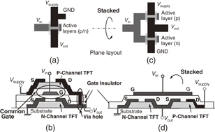
Fig. 2. Planar layout (a) and cross section (b) of stacked complementary inverters and typical layouts (c), (d) of usual planar CMOS.
Download figure:
Standard image High-resolution image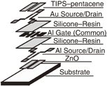
Fig. 3. Schematic fabrication process of stacked CMOS inverters.
Download figure:
Standard image High-resolution imageThe stacked geometry and the common gate electrode are the two main features of such a structure. A complementary inverter was easily realized by connecting the drain electrodes of the p-channel TFT and the n-channel TFT to the output, the source electrode of the p-channel TFT to the supply voltage (Vsupply), and the common gate electrode to the input (Vin) terminal. In fabricating stacked NAND and NOR circuits, a series of vertical and horizontal interconnections of source, drain, and gate lines were formed through via holes formed by a photolithographic technique in the UV curing process of silicone-resin film. Figures 4(a) and 4(b) show the cross section and planar layout of stacked NAND and NOR circuits.

Fig. 4. Planar layout and cross section of stacked (a) NAND and (b) NOR circuits.
Download figure:
Standard image High-resolution image3. Results and discussion
3.1. Static characteristics of p- and n-channel TFTs
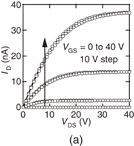
Since the characteristic matching of p- and n-channel TFTs is essential to obtain excellent complementary logic circuits, basic p- and n-channel TFTs of stacked-structure inverter circuits were investigated. In this study, the control of n-channel ZnO TFTs is mainly performed by choosing the UV/O3 treatment temperature (TT = 150–300 °C). At a low TT of 150 °C, ZnO film has a low drain current, low mobility (μ) of 7.6 × 10⁻⁴ cm2 V−1 s−1, and hysteresis in TFT characteristics, as shown in Figs. 5(a) and 5(b). Although the characteristic improvement of ZnO TFTs was realized at a higher TT, the optimized TT of ZnO film was 250 °C for a balanced ZnO TFT characteristic to that of a wet-processed TIPS-pentacene TFT. The static output and transfer characteristics of a top-gate ZnO TFT (at TT = 250 °C) and a bottom-gate TIPS-pentacene TFT are shown in Figs. 6(a) and 6(b), and Figs. 7(a) and 7(b), respectively. The mobility and threshold voltage (Vth) of the ZnO TFT were 1.9 × 10⁻² cm2 V−1 s−1 and 9.3 V, respectively. On the other hand, the average μ of TIPS-pentacene TFTs (25 samples) and Vth were 1.4 × 10⁻² cm2 V−1 s−1 and Vth = 6.5 V, respectively.
Download figure:
Standard image High-resolution image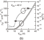
Fig. 5. Static (a) output and (b) transfer characteristics of a top-gate ZnO TFT (UV/O3 treatment temperature at TT = 150 °C).
Download figure:
Standard image High-resolution image
Download figure:
Standard image High-resolution image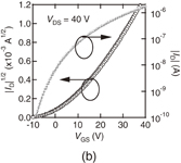
Fig. 6. Static (a) output and (b) transfer characteristics of a top-gate ZnO TFT (UV/O3 treatment temperature at TT = 250 °C).
Download figure:
Standard image High-resolution image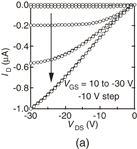
Download figure:
Standard image High-resolution image
Fig. 7. Static (a) output and (b) transfer characteristics of a bottom-gate TIPS-pentacene TFT.
Download figure:
Standard image High-resolution image3.2. Stacked NOT, NAND, and NOR characteristics
The output and transfer characteristics of ZnO and TIPS-pentacene FETs used for NOT, NAND, and NOR circuits in the voltage range of logic operation are shown in Figs. 8(a)–8(d), respectively. Figure 9 shows the voltage transfer characteristics and static voltage gain Vout/Vin of the complementary inverter (NOT circuit). Relatively good performance of complementary inverters was obtained by connecting the vertically stacked p- and n-channel TFTs under the optimized process condition of ZnO TFTs.
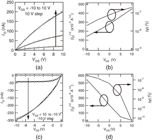
Fig. 8. Output and transfer characteristics of ZnO (a, b) and TIPS-pentacene FETs (c, d) used for NOT, NAND, and NOR circuits in the voltage range of logic operation.
Download figure:
Standard image High-resolution image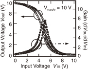
Fig. 9. Voltage transfer characteristics and static voltage gain Vout/Vin of the complementary inverter (NOT circuit).
Download figure:
Standard image High-resolution imageFigures 10(a) and 10(b) show the truth table and the dynamic output voltage (Vout) response of the complementary inverter to a square wave input voltage (Vin: 0–10 V), respectively. The power supply Vsupply was set to 10 V here and the output terminal Vout was correctly inverted according to the input signal Vin. Figures 11(a) and 11(b) show the truth table, input voltage variation, and output voltage characteristics of the stacked-structure NAND circuit, respectively. Figure 12 shows the truth table, input voltage variation, and output voltage characteristics of the stacked-structure NOR circuit, respectively. Both NAND and NOR circuits fabricated by p- and n-channel stacked TFTs based on the solution process showed typical logic operations. Although these logic circuits fabricated here show relatively slow operation of approximately 10 Hz owing to the low driving current, the large parasitic capacitance of the layered structure, and the large margin of interconnection, better operations are expected by designing a proper TFT dimension.

Fig. 10. (a) Truth table and (b) input and output characteristics of stacked complementary inverter.
Download figure:
Standard image High-resolution image
Fig. 11. (a) Truth table and (b) input and output characteristics of stacked NAND circuit.
Download figure:
Standard image High-resolution image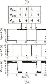
Fig. 12. (a) Truth table and (b) input and output characteristics of stacked NOR circuit.
Download figure:
Standard image High-resolution image
4. Conclusions
NAND and NOR logic circuits composed of stacked structure complementary inverters were fabricated by a low-temperature solution process. Both NAND and NOR circuits fabricated using wet process TIPS-pentacene and ZnO layers showed typical logic operations. These results demonstrate that stacked structure logic circuits based on the solution process have the potential to realize flexible, low-temperature, and large-area integrated circuit applications.
Acknowledgments
This research was partly supported by a "Next Generation Printed Electronics" of the New Energy and Industrial Technology Development Organization (NEDO). We thank ADEKA Corporation for supplying materials used here.