
Abstract
In this study, we have successfully fabricated In–Ga–Zn–O (IGZO) thin-film transistors (TFTs) with various Ga2O3 deposition powers prepared using a two radio-frequency (RF) (ceramics targets: In2O3 and Ga2O3) and one direct-current (DC) (metallic target: Zn) magnetron cosputtering system at room temperature. The carrier concentration for the IGZO films decreases to less than 3 × 1016 cm−3 when the Ga2O3 deposition power is 175 W and Hall mobility decreases from 12.8 cm2 V−1 s−1 and saturates at 4.6 cm2 V−1 s−1 with increasing Ga2O3 deposition power. The increase in the resistivity of the cosputtered films correlates with the decrease in the crystallinity of the InGaZn7O10 phase and the phase transformation from InGaZn7O10 to InGaZn2O5 with increasing Ga2O3 deposition power. With an optimum Ga2O3 deposition power of 150 W, cosputtered IGZO TFTs with a higher, saturated drain current of 4.5 µA, good saturation mobility, μsat of 4.92 cm2 V−1 s−1, Ion/Ioff of 109, a low subthreshold swing (SS) of 0.27 V/decade, and RSD of 30 kΩ have been successfully fabricated.
Export citation and abstract BibTeX RIS
1. Introduction
Transparent amorphous oxide semiconductors (TAOSs) are promising as channel materials of thin-film transistors (TFTs)1,2) and are mainly used for driving TFTs in organic light-emitting diode displays because of their high mobilities (>10 cm2 V−1 s−1) and low process temperatures. Several TAOSs have been reported as good TFT channel materials, including amorphous In–Ga–Zn–O (a-IGZO),1–6) In–Zn–O (IZO),7–9) Zn–Sn–O,10) In–Sn–O (ITO),11) ZnO,12) Al–Zn–Sn–O (AZTO),13) and Al–In–Zn–Sn–O.14) An essential feature of TAOSs is that they are multicomponent materials and therefore demonstrate considerable flexibility in tuning properties for TFTs. Iwasaki et al.15) reported a combinatorial approach to fabricating TFTs by cosputtering three targets including In2O3, Ga2O3, and ZnO in order to clarify the relationship among the a-IGZO channel chemical composition, fabrication conditions, and TFT characteristics. A higher indium (In) content is expected to enhance μFE and increase the on current by a significant increase in the carrier concentration.16–18) A gallium (Ga)-rich film suppresses carrier generation because Ga–O has a higher bonding strength than In–O and is effective in suppressing oxygen vacancy formation.15,16) With increasing Ga content, the optical gap energy of IGZO films increases, and the turn-on voltage of the TFT shifts to positive values.19) Thus, an appropriate addition of Ga is an effective way of attaining a lower off current and a lower carrier concentration. Zinc (Zn) contributes to the reduction in the shallow tail states20) below the conduction band and interface states between gate oxide and channel; thus, the subthreshold swing (SS) is reduced. Cosputtering could provide attractive advantages such as easy control of film stoichiometry, diversity of material selection, and high deposition rate.21) Combinatorial approaches22) were developed to efficiently search for materials having improved performance. Although combinatorial approaches enable us to survey a compositional landscape rapidly, only a few works have been performed in terms of device performance.23,24) By studying magnetron cosputtering with three targets of In2O3, Ga2O3, and Zn, the effects of each element on electrical properties of IGZO semiconductor films and TFT characteristics could be elucidated.
However, few studies have shown the Hall electrical properties and microstructure analysis of IGZO semiconductor films, which were grown using the magnetron cosputtered with three targets of In2O3, Ga2O3, and Zn. In this study, we investigated the effects of the microstructure, chemical composition and phase formation on the electrical properties of cosputtered IGZO films with various Ga2O3 deposition powers and fixed In2O3 and Zn deposition powers. Impacts of the Ga2O3 deposition power on the device characteristics of IGZO TFTs fabricated using a combinational approach were investigated. Finally, the optimum Ga2O3 deposition power for fabricating cosputtered IGZO TFTs is suggested.
2. Method of approach
2.1. Cosputtered IGZO films
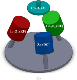
IGZO films were deposited on SCHOTT B270 glass substrates at room temperature using In2O3 (purity, 99.99%), and Ga2O3 (purity, 99.99%) ceramic targets and a Zn (purity, 99.99%) metallic target, all 3 in. in diameter, as shown in Fig. 1(a). Details of the preparation of targets are found elsewhere.25) IGZO films were deposited using a two radio-frequency (RF) (ceramics targets: In2O3 and Ga2O3) and one direct-current (DC) (metal target: Zn) magnetron cosputtering system (LJ-UHV LJ-303CL) at room temperature, in which the Ga2O3 deposition power was varied, in order to verify the effects of Ga2O3 deposition power on the film properties of IGZO channels. The deposition powers of the In2O3 and Zn targets were fixed at 100 and 75 W, respectively. The thicknesses of the IGZO films under different deposition powers were controlled within 180–200 nm. The deposition rates under different deposition powers and the corresponding film thicknesses were measured using an n&k analyzer 1200. The deposition chamber was initially evacuated to 5.3 × 10⁻⁴ Pa, and a fixed Ar gas flow (50 sccm) and O2 gas flow (10 sccm) were introduced into the chamber to maintain the working pressure at 0.67 Pa. After deposition, the samples were annealed at 400 °C at a working pressure of 0.67 Pa for 1 h in N2 ambient of 40 sccm. The resistivity of these films was measured using a four-point probe (Napson RT-80). Hall measurements were performed by the van der Pauw method using a HALL8800 system (Swin). The magnetic field applied during the measurement was 0.68 T. The test samples were cut into 1 × 1 cm2 squares. The surface morphology and chemical composition of the cosputtered IGZO films were respectively investigated using a scanning electron microscope (SEM; JOEL JSM 6500-F) at an operating voltage of 15 kV and an energy dispersive spectrometer (EDS; SEM-S4700). The crystallinity of the IGZO films was also analyzed using glancing angle X-ray diffraction (PANalytical X'Pert Pro) analysis with a Ni-filtered Cu Kα (λ = 1.5418 Å) source at a glancing incident angle of 1°. The scanning range was between 2θ = 20 and 80°.
Download figure:
Standard image High-resolution image
Fig. 1. (a) Target-substrate arrangement of the co-sputtering system and (b) cross-sectional view of the fabricated a-IGZO TFT device.
Download figure:
Standard image High-resolution image2.2. Device fabrication and process flow
The device structure is of the inverted-staggered type, which is the most commonly used structure for active matrix liquid crystal displays (AMLCDs), as shown in Fig. 1(b). To fabricate this structure, a 200 nm Al–Si–Cu film was first deposited by physical vapor deposition (PVD) on a 4 in. silicon substrate capped with a 500-nm-thick thermally grown silicon dioxide (SiO2) film. The metal layer was patterned by photolithography and subsequent wet etching steps to form the gate electrode. Then, a 100 nm tetraethylorthosilicate (TEOS) oxide was deposited by plasma-enhanced chemical vapor deposition (PECVD) as the gate dielectric. Before depositing the IGZO active layer, we presputtered the target with argon flow for 15 min to clean the surface of each target. Subsequently, a 50 nm IGZO film was deposited as the channel layer using three-target cosputtering at various deposition powers of the Ga2O3 target. The deposition powers of the In2O3 and Zn targets were fixed at 100 and 75 W, respectively. The sputtering conditions were the same as the cosputtering condition for the IGZO films. After the deposition, the IGZO channel was postannealed using a backend vacuum annealing furnace at 300 °C at a working pressure of 6.7 Pa for 1 h in N2 ambient of 40 sccm. A 300 nm Al–1.5 wt % Ti S/D metal was then formed by a lift-off process. Afterwards, a lithographic step for defining the active device region was performed. A diluted HCl solution  was used instead to avoid damage and severe lateral etching of the IGZO channel film. In order to achieve contact with the gate electrode, contact etching was performed by wet etching using a buffer oxide etcher (BOE). The channel width (W) was fixed at 400 µm and the designed channel length (L), which is defined as the distance between the source and drain metal pads, was varied from 10 to 100 µm. The electrical measurement of all devices was executed using an Agilent 4156A precision semiconductor parameter analyzer, and the measurement temperature was maintained at 25 °C. Prior to the measurement, all the IGZO TFTs samples used in this study were annealed at 200 °C in air for 40 min on a hot plate to remove excess moisture on TFTs.
3. Results and discussion
3.1. Properties of cosputtered IGZO films at various Ga2O3 deposition powers
The deposition rate of co-sputtered IGZO films increase from 3.7 to 5.4 nm/min with the Ga2O3 deposition power. Figure 2 shows the Hall measurement plot of the cosputtered IGZO films as a function of Ga2O3 deposition power. The carrier concentration and Hall mobility clearly decrease as the Ga2O3 deposition power increases. Specifically, the carrier concentration decreases to less than 3 × 1016 cm−3 when the Ga2O3 power is 175 W and the Hall mobility decreases from 12.8 cm2 V−1 s−1 and saturates at 4.6 cm2 V−1 s−1 with increasing Ga2O3 deposition power. The results indicate that the film resistivity increases considerably with the Ga2O3 deposition power, owing to the lower carrier concentration and lower Hall mobility. However, the carrier concentration and Hall mobility show abnormal values when the Ga2O3 deposition power is 200 W because the film resistance is outside of the range of the Hall measurements. Hu and Gordon26) reported that when the solubility limit reachs 1.0 at. % Ga, the sheet resistance of Ga-doped ZnO films increased gradually. This is due to the reduction in the density of free charge carriers, and the interstitial occupation by Ga atoms, which leads to neutral defects in the structure without contributing a free electron.27)

Fig. 2. Hall measurement plots of co-sputtered IGZO films as a function of Ga2O3 deposition power.
Download figure:
Standard image High-resolution imageFigure 3 shows SEM graphs of the cosputtered IGZO films with increasing Ga2O3 deposition power. It can be observed that the surface morphology shows smaller grains with increasing RF power of Ga2O3. From the SEM studies, a thin film deposited at a higher deposition power yielded smaller grains with an average size of about 10–20 nm as shown in Fig. 3(d) than those of its counterparts, as shown in Figs. 3(a)–3(c). This result is attributed to the increasing number of nucleation centers during the incorporation of the dopant into the host material.26) The reason for the Hall mobility decrease with increasing Ga2O3 deposition power correlates with the decrease in the grain size of IGZO films. Figure 4 shows the In, Ga, and Zn/(In + Ga + Zn) atomic ratios of cosputtered IGZO films as a function of Ga2O3 deposition power. The results were measured by the EDS technique. Although this was only a relative comparison between the conditions, it was clear that the at. % Ga of the deposited films could be controlled by adjusting the sputtering power for the Ga2O3 target. Figure 4 shows that the Zn/(In + Ga + Zn) ratio decreases clearly from 77.1 to 55.1%, whereas the Ga/(In + Ga + Zn) ratio of the deposited films increases noticeably from 8.4 to 28.9% and the In/(In + Ga + Zn) ratio increases slightly from 14.4 to 16% inside the IGZO films as a function of Ga2O3 deposition power. The result in Fig. 2 indicates film resistivity increases considerably with increasing Ga2O3 deposition power. Therefore, the zinc atoms increase the conductivity and gallium atoms enhance the resistivity of the cosputtered IGZO films. Thus, an appropriate addition of Ga is effective in suppressing oxygen vacancy formation and represents an effective way to attain lower carrier concentrations; similar findings have been reported by others researchers.15,16) The results of the chemical composition analyses showed that Ga dopants inside the IGZO films inhibited the grain growth of the prepared films with increasing Ga2O3 power, as shown in Fig. 3.
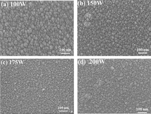
Fig. 3. SEM graphs of co-sputtered IGZO films with Ga2O3 deposition powers of (a) 100, (b) 150, (c) 175, and (d) 200 W.
Download figure:
Standard image High-resolution image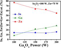
Fig. 4. In, Ga, Zn/(In + Ga + Zn) atomic ratio of the cosputtered IGZO films as a function of Ga2O3 power.
Download figure:
Standard image High-resolution imageIn order to verify the relationships between the crystalline phases and electrical properties of the cosputtered IGZO films, the crystallinities of the IGZO films with various Ga2O3 deposition powers were also analyzed using glancing angle X-ray diffraction; the result are shown in Fig. 5. The IGZO film cosputtered using three targets of In2O3, Ga2O3, and Zn reveals a polycrystalline oxide film. Two crystalline phases of InGaZn7O10 and InGaZn2O5 are shown in the studied films. With increasing Ga2O3 deposition power, the crystallinity of the InGaZn7O10 phase decreases, and the InGaZn7O10 phase is transformed to the InGaZn2O5 phase, which is ascribed to the fact that the  ratio is varied from
  to
to  as the Ga2O3 deposition power increases from 100 to 200 W, as shown in Fig. 4. The increase in the resistivity for the cosputtered films correlates with the decreasing crystallinity of the InGaZn7O10 phase and the phase transformation from InGaZn7O10 to InGaZn2O5 with increasing Ga2O3 deposition power.

Fig. 5. XRD patterns of co-sputtered IGZO films with various Ga2O3 deposition powers of (a) 75, (b) 100, (c) 125, and (d) 150 W.
Download figure:
Standard image High-resolution image3.2. Characteristics of cosputtered IGZO TFTs at various Ga2O3 deposition powers
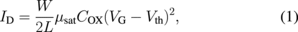
Figure 6 shows the transfer characteristics of the cosputtered IGZO TFTs at VD = 10 V and W/L = 400 µm/10 µm with the deposition power of Ga2O3 varying from 100 to 200 W. The results indicate that the device performance shows an obviously low on-current (Ion)/off-current (Ioff) ratio when the Ga2O3 power is 100 W, which is ascribed to a significantly high Ioff (>10−4 A). However, the Ion/Ioff ratio clearly increases to 1 × 10⁹ when the Ga2O3 power is increased to 150 W, owing to the fact that all the devices exhibit a sufficiently low Ioff of less than 1 × 10⁻¹³ A as the Ga2O3 power is more than 150 W. In terms of the device off-current, compared with that of the IGZO channel prepared at 100 W deposition power, a significant improvement in the off-current (<10−13 A) has been achieved in IGZO TFTs with a channel prepared at a power of 150 W or higher, which is ascribed to the fact that the resistivity in the IGZO channels increases considerably from 0.035 to 0.653 Ω cm with the deposition power of Ga2O3 varying from 100 to 150 W, as shown in Fig. 2. In addition, oxygen vacancies are the main source of free electrons released for transport in the metal–oxide–semiconductors. This is clearly confirmed in the figure as the transfer curves shift positively with increasing Ga2O3 deposition power, since the Ga-rich film tends to suppress carrier generation and oxygen vacancy formation.15,16) Therefore, a higher gate voltage is necessary to accumulate free electrons to form a conductive layer between the source and the drain. Table I shows a summary of the electrical characteristics of the cosputtered IGZO TFTs with various deposition powers of Ga2O3 and W/L = 400 µm/10 µm. The saturation mobility (μsat) was calculated using
where COX and Vth are the capacitance of the TEOS gate insulator and the threshold voltage, respectively. Vth is defined as the intercept voltage with VG from the maximum slope of the respective square-root (sqrt) ID vs VG plot, as shown in Fig. 6. Figures 7(a) and 7(b) show the ID–VD output characteristics of the cosputtered IGZO TFTs (W/L = 400 µm/10 µm) with deposition powers of Ga2O3 of 150 and 200 W, respectively. With an optimum deposition power of Ga2O3 at 150 W, a higher saturated drain current (4.5 µA) at a higher drain voltage is demonstrated at VG − Vth = 8 V, which is ascribed to the existence of sufficient oxygen vacancies for releasing free electrons for transport in cosputtered IGZO semiconductors. By contrast, the output characteristics of IGZO TFTs at a higher Ga2O3 power of 200 W indicate a lower unsaturated drain current at a higher drain, suggesting the lack of strong inversion in a high-resistance IGZO channel. For a low VD, the total resistance (Rtotal) as a function of the designed channel length can be evaluated by the total resistance method conducted in the linear region of the output characteristics of the devices using28–32)

where RCH and RSD are the channel resistance and source/drain (S/D) parasitic resistance, respectively. Figures 8(a) and 8(b) show the extracted Rtotal, RCH, and RSD as a function of gate overdrive with L = 400 and 10 µm for the IGZO TFT devices with deposition Ga2O3 powers of 150 and 200 W, respectively. As can be seen in Fig. 8(a), for the lower Ga2O3 deposition power of 150 W, the RSD (30 kΩ) contribution to Rtotal is negligible regardless of the gate overdrive voltage. On the other hand, for the devices prepared with a higher Ga2O3 deposition power of 200 W, the RSD contribution to device characteristics is not negligible, as shown in Fig. 8(b). Actually RSD (250 kΩ) even approaches RCH at a higher gate overdrive voltage of 8 V, as shown in the figure. The devices prepared with a higher Ga2O3 deposition power of 200 W have a lower drain current at the same gate overdrive voltage owing to the higher RSD, as shown in Fig. 7(b). In addition, Fig. 7(b) indicates the ID–VD output characteristics of the cosputtered IGZO TFTs with a higher Ga2O3 power of 200 W showing the decrease in the unsaturated drain current with increasing drain voltage due to lack of a strong inversion at a high VD in the high-resistance IGZO channel. Therefore, the cosputtered IGZO TFT prepared with a Ga2O3 power of 200 W shows the worst device characteristics, as shown in Table I. It is clear that a higher gate overdrive voltage induces more free electrons to be transported in the channel, which is the main reason for the decrease in channel resistance. Because the cosputtered IGZO films deposited with a higher Ga2O3 power tend to reduce their carrier concentration in the channel, a higher potential barrier height and longer transport paths are expected from the percolation model.2) By controlling the sputtering power of Ga2O3, polycrystalline cosputtered IGZO thin films have been successfully deposited, and the fabricated TFTs revealed good device performance.

Fig. 6. ID–VG transfer characteristics of co-sputtered IGZO TFTs (W/L = 400 µm/10 µm) at VD = 10 V with various Ga2O3 deposition powers.
Download figure:
Standard image High-resolution image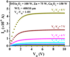
Download figure:
Standard image High-resolution image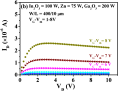
Fig. 7. ID–VD output characteristics of cosputtered IGZO TFTs (W/L = 400 µm/10 µm) with Ga2O3 deposition powers of (a) 150 and (b) 200 W.
Download figure:
Standard image High-resolution image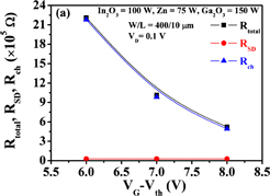
Download figure:
Standard image High-resolution image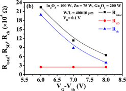
Fig. 8. Extracted Rtotal, Rch, and RSD as a function of gate overdrive voltage of cosputtered IGZO TFTs (W/L = 400 µm/10 µm) with Ga2O3 deposition powers of (a) 150 and (b) 200 W.
Download figure:
Standard image High-resolution image
Table I. Summary of electrical characteristics of co-sputtered IGZO TFTs with various Ga2O3 deposition powers, W/L = 400 µm/10 µm (Deposition powers of In2O3 = 100 W and Zn = 75 W).
| Ga2O3 power (W) | Vth (V) | SS (V/decade) | Iona) (A) | μsat (cm2 V−1 s−1) | Ion/Ioff | RSD (×103 Ω) |
|---|---|---|---|---|---|---|
| 100 | — | — | 4.86 × 10⁻⁴ | — | 2 | — |
| 150 | 6.0 | 0.27 | 1.36 × 10⁻⁵ | 4.92 | ∼109 | 30 |
| 175 | 6.5 | 0.35 | 9.72 × 10⁻⁶ | 4.60 | ∼109 | 100 |
| 200 | 7.8 | 0.45 | 2.80 × 10⁻⁷ | 0.34 | ∼107 | 250 |
a) Ion (VG = 10 V, VD = 10 V).
4. Conclusions
In summary, we found that, with increasing Ga2O3 deposition power, the resistivity of cosputtered IGZO films increases, while the Hall mobility and carrier concentration decrease. Moreover, the deposition rate of the cosputtered IGZO films increases, and the surface microstructure shows a smaller granular size as the deposition power of Ga2O3 increases, which is attributed to the increase in the number of nucleation centers during the incorporation of the Ga dopant into the host IGZO material. Therefore, the smaller granular appearance in the surface indicates a lower mobility. The cosputtered IGZO film reveals a polycrystalline oxide film. The increase in resistivity for the cosputtered films correlates with the decrease in the crystallinity of the InGaZn7O10 phase with increasing Ga2O3 deposition power and the phase transformation from InGaZn7O10 to InGaZn2O5 when the Ga2O3 power is 150 W, which is ascribed to the fact that the  ratio varies from
  to
to  as the Ga2O3 power increases from 100 to 150 W. The results for device characteristics of the cosputtered IGZO TFTs indicate an increase in Vth, SS, and RSD, while a decrease in μsat, Ion, and Ion/Ioff when the deposition power of Ga2O3 increases from 150 to 200 W. With an optimum deposition power of Ga2O3 of 150 W, cosputtered IGZO TFTs with a higher saturated drain current of 4.5 µA, μsat of 4.92 cm2 V−1 s−1, Ion/Ioff of 1 × 10⁹, a low SS of 0.27 V/decade, and RSD of 30 kΩ have been successfully fabricated, owing to the fact that all the devices exhibit a sufficiently low Ioff of less than 10−13 A with the deposition power Ga2O3 being larger than 150 W. By contrast, the ID–VD output characteristics of the cosputtered IGZO TFTs with a higher Ga2O3 power at 200 W indicate decrease in unsaturated drain current with increasing drain voltage due to the higher RSD (250 kΩ) and the lack of a strong inversion in the high-resistance channel. The results of the characteristics analysis of cosputtered IGZO TFTs with an optimum Ga2O3 power indicate that polycrystalline IGZO films could be successfully cosputtered and prepared for applications to transparent thin film transistors.
Acknowledgment
This work was supported in part by the National Science Council Research Project (NSC 100-2221-E-159-009).