
Abstract
We demonstrated a novel and simple approach to obtain a reliable Cu/SiO2 stack. The key is the combination of SiO2 surface doping with Zn and intermixing acceleration by a noble metal catalyst. Zn was incorporated into the SiO2 surface by heat treatment of ZnO/SiO2 stacks. The intermixing layer was formed even when Cu films were deposited at room temperature, and this layer dramatically improved the adhesion between Cu and SiO2.
Export citation and abstract BibTeX RIS
1. Introduction
Reliable and high-precision Cu/SiO2 structures are particularly desirable for microelectromechanical systems and packaging technologies. Many researchers have investigated on the improvement of the adhesion between Cu and SiO2.1–15) Most of these reports indicated that the high-temperature annealing results in the formation of a self-forming intermixing layer at the interface when a Cu alloy was used instead of a pure Cu. It was also indicated that this intermixing layer improves the adhesion strength at the Cu/SiO2 interface. The question is how to form such an intermixing layer. In general, a higher temperature and a longer annealing time are needed, but temperature lowering and process time reduction are preferred to reduce thermal budget as well as fabrication cost.
Previously, we studied the adhesion strength and interfacial nanostructures of Cu/Pd/ZnO/SiO2 stacks.16) The adhesion between Cu and SiO2 was dramatically improved when a 10-nm-thick ZnO layer was used together with Pd particles, where an extremely thin intermixing layer consisting of Cu, Pd, Zn, Si, and O was clearly formed at the interface even when the Cu film was deposited at room temperature. This room-temperature intermixing did not occur when Pd was not present. These results obviously indicate that Pd has a key role in accelerating the intermixing because the phase diagram of ZnO–SiO217) shows that these two phases will react over 1300 °C. We expect that other noble elements also behave the same way and this was left as an interesting subject to study.
In the present study, we tried to generalize the effects of Zn and noble metals on the intermixing acceleration. To achieve this challenge, SiO2 surface was doped with Zn by using a ZnO layer as a Zn source, where the ZnO layers were prepared by different deposition methods. Noble metals, here Pt, Pd, and Pt–Pd, were used to study the effectiveness of noble metals on the intermixing acceleration, where all those metals were deposited only by sputtering to standardize the deposition method. (In our previous study, Pd was deposited by using a sensitization-catalyzation technique that is used in a standard electroless plating.)
2. Experimental procedure
In order to dope SiO2 surface with Zn, thermal diffusion was used. At first, a 150-nm-thick polycrystalline ZnO layer was prepared on SiO2 (fused silica glass) substrates by metalorganic chemical vapor deposition (MOCVD)18) or molecular beam epitaxy (MBE).19,20) These techniques provide device-grade ZnO18,19,21–28) and thus ensure to minimize the interfering effects of ZnO quality, such as crystallinity or impurity incorporation. Deposition temperatures of MOCVD- and MBE-ZnO were 400 °C and room temperature, respectively. The MBE-ZnO/SiO2 stack was then annealed at 350 °C for 60 min. Afterwards, the ZnO layers were removed from the SiO2 substrate by dipping the sample in an acid solution. Noble metal particles of Pt, Pd, or Pt–Pd, were then deposited on the substrate surface by sputtering. We confirmed by using atomic force microscopy that the deposited noble metals are not films but particles. Finally, Cu films were sputtered to a thickness of 200 nm with no intentional substrate heating or cooling.
The adhesion strength was evaluated with a micro-scratch tester (Rhesca CSR-2000) following JIS R3255 specifications, where the load applied to the horizontally vibrating stylus was increased continuously with the traveling displacement of the stylus. The critical adhesion strength was defined as the applied load at which the delamination occurred. The delamination position was determined by optical microscopy. Five different positions were tested for each sample.
Nanostructural observations were performed by using transmission electron microscopy (TEM) and scanning transmission electron microscopy (STEM). Chemical composition analyses were carried out using an energy dispersive X-ray spectrometer equipped to the TEM (TEM–EDX). The samples for cross-sectional TEM and STEM observations were prepared by using a focused ion beam method using Ga ions. TEM–EDX point analyses were carried out at regions that were able to observe a high-resolution image.
3. Results and discussion
3.1. Zn incorporation into SiO2 surface
In order to confirm the incorporation of Zn into the SiO2 surface, the interfaces of ZnO/SiO2 were examined before removing the ZnO layer.
Figure 1 shows TEM images and Zn, Si, and O maps of the interfaces of (a, b) as-deposited MOCVD-, (c, d) as-deposited MBE-, and (e, f) annealed MBE-ZnO/SiO2 stacks. In any stack, a sound interface without defects such as voids and inclusions was formed. An approximately 5-nm-thick interfacial layer having an intermediate contrast between ZnO and SiO2 was clearly observed at the as-deposited MOCVD- and the annealed MBE-ZnO/SiO2 interfaces. The interfacial layer was formed on the SiO2 side of the interface. In the as-deposited MBE-ZnO/SiO2 stack, equi-axed grains were formed on the ZnO side of the interface and their contrast was similar to that of ZnO.

Fig. 1. TEM images and TEM–EDX maps of the interfaces of (a, b) as-deposited MOCVD-, (c, d) as-deposited MBE-, and annealed MBE-ZnO/SiO2 stacks.
Download figure:
Standard image High-resolution imageStrong Zn and Si signals were detected over the entire ZnO and SiO2 regions, respectively. The Zn and Si signal intensities decreased slightly in the interfacial layer regions of the as-deposited MOCVD- and the annealed MBE-ZnO/SiO2 stacks [Figs. 1(b) and 1(f)], whereas the as-deposited MBE-ZnO/SiO2 stack showed very sharp transition between the Zn and Si intensities [Fig. 1(d)]. These results indicate that Zn was diffused approximately 5 nm into the SiO2 when the samples were processed at high temperatures; i.e., the SiO2 surface was doped with Zn by heat treatment.
3.2. Phase identification of the Zn-doped SiO2
In order to identify the phases of the interfacial layer, high-resolution TEM (HRTEM) observations and TEM–EDX analyses were carried out. Figure 2 shows a HRTEM image of the interfacial layer formed at the ZnO/SiO2 interface. A typical amorphous structure having no fringe contrast can be observed in the SiO2 region. The lattice image is clearly observed in the interfacial layer regions as in the ZnO region, obviously proving that the interfacial layer is crystalline. Figure 3(a) shows a high-angle annular dark field (HAADF) image of the interfacial layer. The interfacial layer consists of high-contrast regions [A in Fig. 3(b)] and low-contrast regions [B in Fig. 3(b)], indicating that the interfacial layer is not a single phase.

Fig. 2. High-resolution TEM image of the ZnO/SiO2 interface.
Download figure:
Standard image High-resolution image
Download figure:
Standard image High-resolution image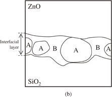
Fig. 3. (a) HAADF image of the ZnO/SiO2 interface. (b) Schematic illustration of (a). A- and B-regions indicate relatively higher and lower contrast regions in the HAADF image, respectively.
Download figure:
Standard image High-resolution imageTable I shows EDX point analysis results taken from the A- and B-regions. Zn, Si, and O were detected in both the regions but the atomic ratio among Zn, Si, and O was different. The A-region had a high Zn concentration, whereas the atomic percentage of Si was almost half of that of O. We suppose that the A-region is Zn-containing SiO2 [SiO2(Zn)] (discussed in Sect. 3.4). The atomic ratio among Zn, Si, and O in the B-region was  which fairly agrees with the stoichiometry of the equilibrium Zn2SiO4 phase.
Table I. EDX results of higher and lower contrast regions formed in interfacial layer.
| Atomic percentage | |||
|---|---|---|---|
| Zn | Si | O | |
| A-region (higher contrast region) | 42 | 18 | 40 |
| 46 | 16 | 38 | |
| 36 | 21 | 43 | |
| B-region (lower contrast region) | 27 | 17 | 56 |
| 29 | 19 | 52 | |
| 33 | 17 | 50 | |
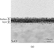
Figure 4 shows (a) a cross-sectional TEM image and (b) Zn, Si, and O maps of the SiO2 surface taken after removing the ZnO layer. The TEM image exhibits the presence of an extremely thin surface layer different from the original SiO2 substrate. These EDX maps indicate that the surface layer consists of Zn, Si, and O, and this composition distribution was similar to that of the interfacial layer formed at the ZnO/SiO2 interface by heat treatment [Figs. 1(b) and 1(f)]. This means that the interfacial layer remained at the SiO2 surface as a Zn-doped layer even after the original thick ZnO layer being removed.
Download figure:
Standard image High-resolution image
Fig. 4. (a) TEM image and (b) TEM–EDX maps of SiO2 surface after the removal of ZnO layer.
Download figure:
Standard image High-resolution image3.3. Adhesion improvement
Noble metal particles (Pt in this case) and Cu films were deposited on the Zn-surface-doped SiO2 and non-doped SiO2. The adhesion strengths of these stacks were shown in Table II. When the non-doped SiO2 was used, the average adhesion strength was approximately 25 mN. This value was higher than that of the Cu/SiO2 stack (5.2 mN29)) but was not remarkably increased. On the other hand, when the Zn-surface-doped SiO2 was employed, no delamination occurred even when the applied load was increased to 500 mN, which is identical to the fracture value of the SiO2 substrate. This indicates that the doping of SiO2 surface with Zn was effective for improving the adhesion at Cu/SiO2 interface.
Table II. Adhesion strengths (mN) of Cu/noble metal/non-doped SiO2 and Cu/noble metal/Zn-doped SiO2 stacks. In this case, the noble metal is Pt.
| Cu/noble metal/non-doped SiO2 | Cu/noble metal/Zn-doped SiO2 |
|---|---|
| 26 | >500 |
Table III shows adhesion strengths of Cu sputtered on the Zn-doped SiO2. When no noble metals were used (Cu/Zn-doped SiO2), the average adhesion strength was approximately 50 mN. This value was ten times higher than the adhesion strength of a Cu/SiO2 stack.29) This means that the SiO2 surface doping with Zn is also effective for improving the adhesion between Cu and SiO2; however, this adhesion strength of 50 mN is not high enough. In contrast, no film delamination occurred in any stacks when the noble metals were inserted between the Cu and the Zn-doped SiO2. This proves that Pt, Pd, and Pt–Pd particles are effective catalysts, and, moreover, the combination of the Zn dope and the noble metal catalyzation enhances the adhesion between Cu and SiO2.
Table III. Adhesion strengths (mN) of Cu on Zn-doped SiO2.
| Cu/Zn-doped SiO2 | Cu/Pt/Zn-doped SiO2 | Cu/Pd/Zn-doped SiO2 | Cu/Pt–Pd/Zn-doped SiO2 |
|---|---|---|---|
| 49 | >500 | >500 | >500 |
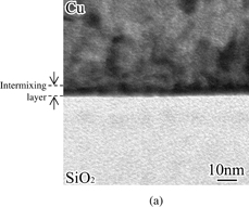
A cross-sectional TEM image and EDX maps of the interface of the Cu/Pt/Zn-doped SiO2 stack are shown in Fig. 5. An extremely thin (less than 10 nm) layer was clearly formed at the interface. Strong Cu signals were detected throughout the Cu film region and a slight decrease in their intensity was observed in the interfacial layer region. Pt signal intensity was high in the interfacial layer and become weaker on the Cu side of the Cu/interfacial layer interface. Zn signals were observed either in the interfacial layer or in the Cu film. Both Si and O signals have a constant intensity in the SiO2 region and become weaker in the interfacial layer region. Quantitative analysis using EDX point probing indicates that the composition of this interfacial layer is Cu42Pt18Zn0.8Si15O22, meaning that intermixing of all the elements existing in the interface occurred. From these observations, it is safely said that the formation of this intermixing layer results in the adhesion improvement. In the previous study, the formation of such an intermixing layer was observed when we used Pd as a catalyst, which shows the intermixing acceleration.16)
Download figure:
Standard image High-resolution image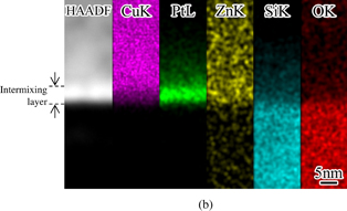
Fig. 5. (a) TEM image and (b) TEM–EDX maps of the interface of a Cu/Pt/Zn-doped SiO2 stack.
Download figure:
Standard image High-resolution image3.4. Formation of intermixing layer
As mentioned above, it was found that the interfacial intermixing occurs at room-temperature by adopting Zn doping and noble metal catalyzation. In addition, the formation of this intermixing layer resulted in the adhesion enhancement. In this section, based on our observation results and the phase diagrams, the reaction route at the interface and the formation mechanism of the intermixing layer are discussed.
3.4.1. ZnO–SiO2 reaction at 300–400 °C
Figure 6 shows a Zn–Si–O ternary diagram at 300–400 °C on which the compositions of the observed phases are plotted. The tie lines show possible routes of the interfacial reactions drawn based on our observations and on a ZnO–SiO2 binary phase diagram,17) as discussed below. When ZnO layers were deposited on SiO2 at 350 °C or when a ZnO/SiO2 stack was annealed at 400 °C, SiO2(Zn) [ (Table I)] and Zn2SiO4 phases, which are plotted in Fig. 6 with solid symbols, were formed at the interface. This layer remained as the surface layer after ZnO removal. The SiO2(Zn) lie on the Zn–SiO2 tie line and the Zn2SiO4 lie on the ZnO–SiO2 tie line. This fairly proves that the SiO2(Zn) phase was formed by the reaction between Zn and SiO2, and the Zn2SiO4 phase was produced by a direct reaction between ZnO and SiO2. The ZnO–SiO2 phase diagram17) shows that ZnO and SiO2 react over 1300 °C and forms Zn2SiO4. Our process temperature was lower than this temperature, therefore, the Zn2SiO4 was formed by diffusion reaction.
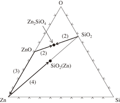
Fig. 6. Zn–Si–O ternary diagram at 300–400 °C plotting the compositions of the observed phases.
Download figure:
Standard image High-resolution imageThe reaction between ZnO and SiO2 does not produce other compounds (2ZnO + SiO2 → Zn2SiO4). Therefore, based on our observations, we formulated a possible overall reaction as follows:

where the coefficient of Zn is introduced as 2Zn to satisfy the stoichiometry of Zn. The bracket of Zn shows that Zn is free metal and dissolves in or coexists with the SiO2. The formation of the Zn2SiO4 phase cannot be excluded but is not necessarily assumed here because 1) SiO2 is very stable and inert, at least, compared to ZnO, 2) the presence of such a compound or Zn–SiO2 phase diagrams is not known to the extent of the author's survey, and 3) the formation of Zn2SiO4 required more phase equilibriums some of those may not satisfy the phase rule.
Reaction (1) indicates that the molar ratio of the formed Zn2SiO4 and the SiO2(Zn) is  and that more ZnO is consumed in the reaction than SiO2. Indeed, from the TEM–EDX analyses, the volumes of these phases are almost identical apart from the molar density of these phases. The stoichiometry also shows that free Zn forms and dissolves in SiO2. As a result, as observed (Table I), the Zn2SiO4 and the SiO2(Zn) coexist at the interface.
This reaction requires reductive chemistry or release of oxygen. It is well-known that vapor deposited ZnO has oxygen vacancies especially at elevated temperatures. Either when oxygen-deficient ZnO reacts or when the formed oxygen diffuses through or stuff oxygen vacancies, reaction (1) is satisfied in terms of the presence of O on the right-hand side.
Elementary reactions of reaction (1) can be expressed as follows:


In fact, the above formulae simply indicate that ZnO is decomposed to Zn and O. Presumably, reaction (2) ignites these reactions to proceed. Once Zn diffuses into SiO2, oxygen in ZnO becomes less and promotes oxygen diffusion. This atomic agitation will accelerate reaction (2). Finally, schematic diagrams of the above-mentioned reactions are shown in Fig. 7.
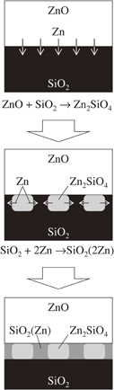
Fig. 7. Schematic diagrams of the formation of Zn2SiO4 and SiO2(Zn) phases at 300–400 °C.
Download figure:
Standard image High-resolution image3.4.2. Pt catalyzed reactions during room-temperature Cu deposition
It should be noted that the Cu42Pt18Zn0.8Si15O22 phase was formed at the Cu/SiO2 interface at room temperature (Fig. 5). The Zn–Si–O composition of this phase is Zn2.1Si39.7O58.2 (open symbol in Fig. 8). This composition is very close to the Si–O tie line and has a Si–O ratio close to  . Therefore, we can safely say that this phase is an oxygen-deficient silicon oxide, presumably Si2O3 (SiO2
 SiO) that contains impurity Zn. The reactions can be expressed as the following formulae:


Reaction (5) is a Pt-catalyzed reaction that generates (free) oxygen and (free) Zn. Zn is well miscible in Cu,30) so that the repelled Zn dissolves into the depositing Cu (Fig. 9). The dissolution of Zn is clearly seen in the EDX map of Zn, where Zn exists in the Cu film region [Fig. 5(b)]. Reaction (6) simply expresses the dissolution of Zn in Cu, and thus the stoichiometric balance of Zn is not taken into account here.
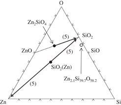
Fig. 8. Zn–Si–O ternary diagram at room temperature plotting the compositions of the observed phases.
Download figure:
Standard image High-resolution image
Fig. 9. Schematic diagrams of the behavior of Zn at room temperature.
Download figure:
Standard image High-resolution image
Free oxygen may also dissolve in Cu but the presence of oxygen is not clearly confirmed in our EDX analyses. O atoms in the above reactions are introduced nominally to satisfy the stoichiometry in terms of our EDX observations. Another subject left is a fact that Pt is dissolved in the intermixing layer. We used Pt particles, whereas the Pt was completely mixed with the other elements after the Cu deposition. This was observed in our previous study using Pd.16) There is still a large possibility that noble metals form other compounds such as oxides and co-dissolve to the existing oxides besides their catalytic role.
4. Conclusive summary
In the present study, an intermixing layer was formed at the Cu/SiO2 interface by depositing noble metal particles, such as Pt, Pd, and Pt–Pd, prior to Cu deposition. This intermixing layer improved the adhesion at the interface dramatically. No remarkable adhesion improvement was observed and no intermixing occurred when no noble metal was employed. It cannot be overstressed that these reactions proceed at room temperature. This happened even when the Cu films were formed by using electroless plating at room temperature,16) indicating that formation of intermixing layer does not depend on Cu deposition method. As well known, Cu and SiO2 do not generally react at room temperature. Obviously, the noble metals lead to the intermixing acceleration, very likely by their catalytic effect.
Acknowledgements
We acknowledge Professor Yoichi Nabetani and Professor Tsutomu Muranaka of University of Yamanashi for providing ZnO films. This research was financially supported by a Grant-in-Aid for Young Scientists (B) (25820122) from the Japan Society for Promotion of Science (JSPS).