
Abstract
Resistive switching memory, flexible electronics equipment, and graphene-oxide-based devices have attracted much attention recently because of their possible application in next-generation electronic devices. In this study, a graphene-oxide-based flexible resistive switching memory is proposed. The flexibility and nonvolatility of the flexible device are demonstrated. A possible resistive switching filamentary model of the flexible device is also proposed. The experimental results indicate that the proposed graphene-oxide-based device is promising for use in next-generation nonvolatile memory and flexible electronics equipment.
Export citation and abstract BibTeX RIS
1. Introduction
First, resistive switching memory has been extensively studied because of its simple structure, easy operation, high speed, and low cost.1–9) In the near future, the mainstream of nonvolatile memory, flash memory, will approach its physical and technical limitations;10) therefore, resistive switching memory is proposed to replace flash memory in the future. Second, flexible electronics equipment with light weight and flexibility is also attracting much attention for use in next-generation portable equipment.11–15) Third, graphene and graphene oxide (GO) are becoming popular because of their good electrical properties and flexibility.10,16–34) Hence, graphene and GO are highly suitable for use in flexible electronics equipment. For the above-mentioned three reasons, a GO-based flexible resistive switching memory is studied in this work.
Chen et al. reported a HfOx-based resistive switching memory improved by inserting single-layer graphene.16) Wu et al. reported a single graphene sheet for nonvolatile memory application. They proposed that the observed switching effect originates from the local oxidation at the graphene/electrode interface.17) In addition, Chakrabarti et al.18) and Yang et al.19) proposed resistive switching memories with graphene electrodes. Furthermore, much research is also focused on the GO film. In the previous reports, the GO film was employed as a resistive switching layer on Si and glass substrates.10,20–28) The resistive ratio of a high-resistance state (HRS) to a low-resistance state (LRS) was approximately from 102 to 104, and the retention time was from 103 to 104 s in those reports. Furthermore, the GO film was fabricated on plastic substrates, to demonstrate its flexibility, for the first time in 2010.29,30) The resistive ratio was almost unchanged at the bending radius of 4 mm. The resistances of the HRS and LRS showed no appreciable degradation up to 1000 repetitions of the bending test. In addition, Wang et al. reported a GO-based device on a plastic substrate and demonstrated its resistive switching speed.31) Yuan et al. also reported a GO-based device on a plastic substrate and demonstrated its resistive switching behavior, but the flexibility of the device was not studied.32)
For the three reasons mentioned in the first paragraph and on the basis of the literature review in the second paragraph, a GO-based flexible resistive switching memory is studied in this work. The Al/GO/Cu/poly(ether sulfone) (PES) structural device is employed in this study. The resistive switching properties and uniformity of the GO-based flexible devices before bending (BB), during bending (B1), after bending (AB1), while bending twice (B2), and after bending twice (AB2) are investigated to demonstrate the flexibility. A possible resistive switching filamentary model of the GO-based device is proposed. Furthermore, the nonvolatility of the GO-based device is also demonstrated. The experimental results indicate that the proposed GO-based flexible resistive switching memory is promising for use in next-generation flexible electronics.
2. Experimental procedure
2.1. Graphite oxide powder
First of all, 120 ml of concentrated sulfuric acid was cooled to 5 °C in an ice bath, and 5 g of graphite powder and 15 g of potassium permanganate were added to the iced sulfuric acid. Because of the exothermic phenomenon, the temperature of the solution would increase. It was controlled to be under 35 °C, and the solution was stirred for 2 h. Second, 250 ml of deionized water was added to the solution, and the solution was stirred for another 2 h. Third, 20 ml of hydrogen peroxide and 700 ml of deionized water were added to the solution, and the solution was stirred for 12 h. Then, the solution was filtered through filter paper. Next, 100 ml of hydrochloric acid and 1000 ml of deionized water were used to wash the residual slurry on the filter paper to remove metal ions. After that, 1000 ml of deionized water was used to wash the slurry again. Finally, the slurry was dried, and graphite oxide powder was obtained.
2.2. Graphene oxide suspension
First, the graphite oxide powder and deionized water were mixed and stirred for 10 min. Second, the solution was ultrasonically agitated for 30 min, and then the GO was flaked after collision. Third, the solution was centrifuged for 30 min to precipitate the turbid solution. After that, the clear solution at the top was taken out, and then the clear solution was ultrasonically agitated and centrifuged for 2 h and 15 min, respectively. Finally, the clear solution at the top was taken out again, and a GO suspension was obtained.
2.3. Device fabrication and measurement
First of all, a Cu bottom electrode was deposited on a 200-µm-thick PES substrate by RF-magnetron sputtering at room temperature. Second, the GO suspension was spin-coated on to the Cu layer, and the GO film was then dried in air for 24 h. Then, the second GO layer was fabricated by the same method on the first GO layer. The two layers of the GO film were spin-coated sequentially to prevent the formation of through-pinholes. The total thickness of the GO film was approximately 30 nm. Finally, Al top electrodes 150 µm in diameter defined by a shadow mask were deposited on the GO film by sputtering at room temperature to form the Al/GO/Cu/PES structural devices. In addition, the GO/Cu layers were also deposited on a SiO2/Si substrate for the analyses by X-ray photoelectron spectroscopy (XPS) and atomic force microscopy (AFM). The resistive switching and bending characteristics of the GO-based flexible devices were recorded using a Keithley 2400 source meter at room temperature. Throughout the electrical measurements, voltage signals were applied to the Al top electrode while the Cu bottom electrode was grounded. For the bending test, the GO-based flexible devices were bent to a 5 cm radius of curvature for electrical measurements, and then the devices were returned to being flat. The corresponding tensile strain on the surface of the substrate was 0.2%.
3. Results and discussion
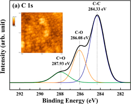
Figure 1(a) shows the C 1s XPS spectrum of the GO film. The peaks of C=O, C–O, and C–C bonds are at 287.93, 286.08, and 284.33 eV, respectively, which are the binding energies that represent the GO film.33) Figure 1(b) shows the O 1s XPS spectrum of the GO film. The film exhibits the peaks of C–OH, C–O, O–H, and C=O bonds at 533.73, 532.43, 531.48, and 530.48 eV, respectively. These binding energies also represent the GO film.34) Therefore, it is demonstrated that the GO film is successfully spin-coated on to the Cu bottom electrode. In addition, the inset of Fig. 1(a) shows the AFM image of the spin-coated GO film, where a smooth surface can be seen. The inset of Fig. 1(b) shows an actual photograph of the GO-based flexible devices.
Download figure:
Standard image High-resolution image
Fig. 1. (a) C 1s and (b) O 1s XPS spectra of the GO film. Inset of (a) is the AFM image of the GO film. Inset of (b) is an actual photograph of the GO-based flexible devices.
Download figure:
Standard image High-resolution imageFigure 2 depicts the typical resistive switching current–voltage (I–V) curves of the Al/GO/Cu/PES flexible devices BB, B1, AB1, B2, and AB2. Before the resistive switching, a large positive bias voltage with current compliance at 5 mA must be applied to activate the flexible devices. This activation is called the forming process (not shown here). After that, the memory state of the devices can be reset from the LRS to the HRS by applying negative bias voltage without current compliance. In addition, the memory state can be set from the HRS back to the LRS by applying positive bias voltage with current compliance at 5 mA. All the flexible devices exhibit similar resistive switching behavior, and the yield of all the flexible devices is over 71%. In addition, the set voltages of the flexible devices decrease with increasing number of bending times. However, the HRS currents of the flexible devices only slightly increase with increasing number of bending times.
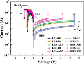
Fig. 2. Typical resistive switching I–V curves of the GO-based flexible devices BB, B1, AB1, B2, and AB2.
Download figure:
Standard image High-resolution imageFigure 3(a) exhibits the cumulative probabilities of the currents for these flexible devices in the HRS and LRS measured at 0.1 and −0.1 V, respectively. It can be observed that the LRS currents are almost unchanged, but the HRS currents slightly increase with increasing number of bending times. Although the resistance ratios of the HRS to LRS decrease with increasing number of bending times, they become stable and uniform and remain at approximately two orders of magnitude after the bending test. Figure 3(b) shows the cumulative probabilities of reset and set voltages of these flexible devices. The reset voltages are very stable at approximately −0.5 V, and the set voltages of the flexible devices decrease with increasing number of bending times. The resistive switching parameters, including the HRS and LRS currents measured at ±0.1 V, reset and set voltages, and switching cycles, are shown in Table I. Generally speaking, the resistive switching becomes stable after the bending test, demonstrating the flexibility of the GO-based device. Nevertheless, the switching cycles slightly decrease with increasing number of bending times; it must be improved in the future to enable practical application in flexible electronics.
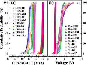
Fig. 3. Cumulative probabilities of (a) the HRS and LRS currents measured at 0.1 and −0.1 V, respectively, and (b) the reset and set voltages of the GO-based flexible devices BB, B1, AB1, B2, and AB2.
Download figure:
Standard image High-resolution imageTable I. Average and standard deviations of the HRS and LRS currents measured at ±0.1 V, and reset and set voltages of the flexible devices BB, B1, AB1, B2, and AB2. The switching cycles of the flexible devices are also indicated.
| Avg./Std. | BB | B1 | AB1 | B2 | AB2 |
|---|---|---|---|---|---|
| IHRS × 10−6 (A) | 1.30/3.06 | 2.41/1.75 | 6.85/7.41 | 19/4.26 | 35.9/6.63 |
| ILRS × 10−3 (A) | 4.40/1.62 | 3.98/1.66 | 7.52/0.97 | 4.60/1.10 | 5.59/2.26 |
| VSet (V) | 3.49/2.03 | 3.12/1.31 | 3.03/0.72 | 2.89/2.03 | 2.40/1.74 |
| VReset (V) | −0.56/0.21 | −0.65/0.21 | −0.46/0.15 | −0.66/0.16 | −0.67/0.26 |
| Switching cycles | 275 | 166 | 179 | 172 | 91 |
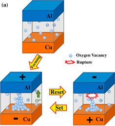
Figure 4 shows a possible resistive switching model of the flexible devices. Initially, the resistance of the GO film is very high, and the leakage through the oxygen vacancies in the GO film is very low. When a large positive bias voltage is applied to the Al top electrode, the positively charged oxygen vacancies will migrate through the GO film to form a connection with the Cu bottom electrode, as shown in Fig. 4(a). The connection causes the formation of a conductive filament,15) which is called the forming process. Hence, the memory state of the device is set to the LRS. In addition, when a negative bias voltage is applied, a large current flows through the filament. The filament is heated by accumulated local Joule heat, and then some vacancies in the weakest region are filled by oxygen atoms, leading to the rupture of the filament,15) as shown in Fig. 4(a). Therefore, the memory state of the device is reset from the LRS to the HRS. On the other hand, the filament can be re-established by applying a positive bias voltage. The memory states can be stably switched between the LRS and HRS repeatedly. The discussion in Figs. 2 and 3 point out that the HRS currents of the flexible devices slightly increase, and the set voltages of the flexible devices decrease with increasing number of bending times. The explanation for this is that while bending is being performed on the flexible device, some defects are generated in the GO film, as shown in Fig. 4(b). Therefore, the HRS currents slightly increase because of the existence of the new defects in the GO film. In addition, the defects participate in resistive switching, so the conductive filament is formed more easily. Then, the set voltages decrease after the bending test. In conclusion, the resistive switching becomes stable after the bending test because the new defects participate in resistive switching.
Download figure:
Standard image High-resolution image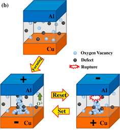
Fig. 4. Possible resistive switching model of the GO-based flexible devices. (a) Before the bending test and (b) after the bending test.
Download figure:
Standard image High-resolution imageFigure 5 indicates the retention time of the GO-based flexible devices BB, B1, AB1, B2, and AB2. Except for the BB device, the two memory states of the devices are stable for over 105 s, and the resistance ratios of the LRS to HRS currents remain at approximately two orders of magnitude. The experimental results demonstrate the nonvolatility of the GO-based flexible device.

Fig. 5. Retention time of the GO-based flexible devices BB, B1, AB1, B2, and AB2.
Download figure:
Standard image High-resolution image
4. Conclusions
Al/GO/Cu/PES flexible resistive switching memory is proposed in this study. The resistive switching characteristics of the GO-based flexible devices BB, B1, AB1, B2, and AB2 are investigated. The resistive switching of the flexible devices can be stably reproduced for over 90 cycles. Although the resistance ratios of the HRS to LRS decrease with increasing number of bending times, the ratios become stable and uniform and remain at approximately two orders of magnitude after the bending test. Therefore, the flexibility of the GO-based resistive switching memory is demonstrated. In addition, the retention time of the flexible devices is over 105 s, so the nonvolatility of flexible devices is also demonstrated. The experimental results indicate that the proposed Al/GO/Cu/PES flexible resistive switching memory may be used in next-generation nonvolatile memory and flexible electronics equipment.
Acknowledgement
This work was supported by the National Science Council of Taiwan under project numbers NSC 101-2221-E-259-020 and NSC 102-2221-E-259-032.