
Abstract
The annealing of an AlN buffer layer in a carbon-saturated N2–CO gas on a sapphire substrate was investigated. The crystal quality of the buffer layer was significantly improved by annealing at 1650–1700 °C. An AlN buffer layer with a thickness of 300 nm was grown by metalorganic vapor phase epitaxy (MOVPE), and was annealed at 1700 °C for 1 h. We fabricated a 2-µm-thick AlN layer on the annealed AlN buffer layer by MOVPE. The full widths at half maximum of the (0002)- and ( )-plane X-ray rocking curves were 16 and 154 arcsec, respectively, and the threading dislocation density was 4.7 × 108 cm−2.
Export citation and abstract BibTeX RIS

Content from this work may be used under the terms of the Creative Commons Attribution 4.0 license. Any further distribution of this work must maintain attribution to the author(s) and the title of the work, journal citation and DOI.
AlN has attracted attention for applications in the deep-ultraviolet (UV) region because of its wide direct band gap and excellent thermal and chemical stability.1–3) However, high-density threading dislocations exist in AlN epitaxial films owing to the large lattice and thermal mismatch between AlN and substrates such as sapphire.4) Therefore, the control of AlN growth near the interface between the AlN and sapphire substrate is one of the most important issues in the realization of high-efficiency UV devices.5,6) To prevent the generation of threading dislocations in the AlN epitaxial layer, the nucleation layer has been controlled.7–12) However, the AlN crystal quality can still be improved by optimizing the nucleation conditions.
Nitridation of a sapphire surface was reported using a carbon-saturated N2–CO gas mixture at a high temperature.13,14) Additionally, in the case of GaN grown on sapphire substrates, the solid-phase epitaxy of nucleation layers, such as GaN and AlN, by annealing is commonly used to improve the crystal quality of GaN films.15–17) However, there are only a few reports on the effects of annealing AlN buffer layers on AlN growth.
In this work, we studied the effects of annealing an AlN buffer layer in a carbon-saturated N2–CO mixture on the growth of high-quality AlN on a sapphire substrate. The effects of annealing were investigated as a function of the AlN buffer layer thickness and annealing temperature.18)
AlN epilayers were grown on c-plane sapphire substrates by metalorganic vapor phase epitaxy (MOVPE). Trimethylaluminum (TMAl) and ammonia (NH3) were used as the Al and N precursors, respectively. Prior to the growth, the substrates were cleaned in H2 ambient at TClean = 1100 °C for 10 min. AlN buffer layers with thicknesses of tBuf = 100–1000 nm were grown at TBuf = 1150–1200 °C under a pressure of 30 Torr. Subsequently, the AlN buffer layers were thermally annealed in a carbon-saturated N2–CO gas mixture at 1500–1750 °C for 2 h. A graphite resistance furnace was used for the annealing experiments. Table I shows the partial pressures of N2 and CO gases as a function of annealing temperature.13,14) The flow rate of the gas mixture was 2.0 L/min during the annealing. In order to prevent desorption of the AlN layer, the partial pressure of N2 was chosen to be 5–15% rich of the phase equilibrium condition of AlN+C and Al2O3+C. For annealing with partial pressures of N2: 0.9 atm and CO: 0.1 atm at 1700 °C, the surface of AlN buffer layers became rough because of the Al2O3 decomposition from the interface of the AlN layer and the sapphire substrate.
Table I. Annealing condition of AlN buffer on sapphire using N2–CO gas mixture.14)
| Annealing temperature (°C) | Partial pressure (atm) | |
|---|---|---|
| N2 | CO | |
| 1500 | 0.9 | 0.1 |
| 1550 | 0.85 | 0.15 |
| 1600 | 0.8 | 0.2 |
| 1650 | 0.7 | 0.3 |
| 1700 | 0.6 | 0.4 |
| 1750 | 0.5 | 0.5 |
Finally, high-temperature (HT) AlN layers with a thickness of tHT = 2 µm were grown on the AlN buffer layers in a H2–N2 mixture at THT = 1450 °C under 30 Torr by the MOVPE. The growth rate of the HT-AlN layers was 1 µm/h. The crystalline quality of the AlN was characterized by X-ray diffraction analysis with asymmetric Ge(220) and symmetric Ge(440) monochromators and transmission electron microscopy (TEM), and the surface morphology was examined by atomic force microscopy (AFM).
Figure 1 shows AFM images of the AlN buffer layers with tBuf = 200, 300, and 1000 nm grown at TBuf = 1150 °C before and after annealing at TAn = 1650 °C. The root-mean-square (RMS) surface roughness of the AlN buffer layers increases as the thickness AlN increases. After annealing the AlN buffer layers, the surface morphologies were markedly changed, and the RMS values were improved. The surfaces of the AlN buffer layers with a thickness of 300 nm or less were smooth. In particular, the RMS value of the annealed AlN buffer layer with tBuf = 300 nm (e) was 0.49 nm, and atomic steps were observed on its surface. However, the surface of the AlN buffer layer with tBuf = 1000 nm was rough even after annealing.
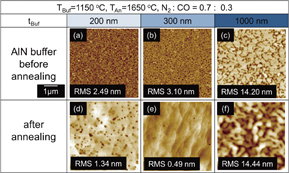
Fig. 1. AFM images of AlN buffer layers with various thicknesses grown at TBuf = 1150 °C (a–c) before and (d–f) after annealing at TAn = 1650 °C: (a, d) tBuf = 200 nm, (b, e) tBuf = 300 nm, and (c, f) tBuf = 1000 nm. The scanning area in the AFM is 5 × 5 µm2.
Download figure:
Standard image High-resolution imageThe full widths at half maximum (FWHMs) of the (0002)- and ( )-plane X-ray rocking curves (XRCs) using an asymmetric Ge(220) monochromator for the AlN buffer layers with thicknesses of 100–1000 nm, which were grown at TBuf = 1150 °C and annealed at TAn = 1650 °C, are shown in Figs. 2(a) and 2(b), respectively. Compared with those for the samples before annealing, the FWHMs of the XRCs for the samples after annealing were significantly decreased. This indicates that the crystalline quality of AlN was improved by annealing. The minimum FWHM of the (0002)-plane XRC was obtained in the sample with tBuf = 300 nm and gradually increased with increasing tBuf. The FWHMs of the (0002)- and (
 )-plane XRCs for the sample with tBuf = 300 nm were 68 and 421 arcsec, respectively.

Download figure:
Standard image High-resolution image
Fig. 2. FWHMs of (a) (0002)- and (b) ( )-plane XRCs for AlN buffer layers with various thicknesses grown at TBuf = 1150 °C before and after annealing at TAn = 1650 °C.
Download figure:
Standard image High-resolution imageFigure 3 shows AFM images of the AlN buffer layers with tBuf = 300 nm grown at TBuf = 1150 °C before and after annealing at TAn = 1500–1700 °C. The surface of the AlN buffer layer without annealing was observed to have small grains, and the RMS value was 3.1 nm. After annealing at temperatures above 1500 °C, the RMS value markedly decreased with increasing annealing temperature. The RMS value for the AlN buffer layers after annealing at TAn = 1650 °C was 0.49 nm. Figure 4 shows the FWHMs of the (a) (0002)- and (b) ( )-plane XRCs for the AlN buffer layers after annealing at various temperatures. The dotted line shows the FWHM of the XRC for the AlN buffer layer before annealing. The FWHM of the (0002)-plane XRC decreased after annealing but increased at temperatures above 1650 °C. The FWHM of the (
 ) plane XRC monotonically decreased with increasing annealing temperature up to 1700 °C but increased at 1750 °C. For the AlN buffer layer annealed at 1750 °C, the FWHMs of the (0002)- and (
 )-plane XRCs increased, and the surface became rough owing to the decomposition of AlN. It was considered that the surface roughness was caused by the thermal decomposition of the AlN buffer layer during annealing. This phenomenon has also been observed in AlN films formed by the thermal nitridation of sapphire substrates.14,19)

Fig. 3. AFM images of the AlN buffer layers with tBuf = 300 nm grown at TBuf = 1150 °C before and after annealing at TAn = 1500–1700 °C. The scanning area in the AFM is 5 × 5 µm2.
Download figure:
Standard image High-resolution image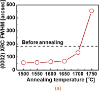
Download figure:
Standard image High-resolution image
Fig. 4. FWHMs of (a) (0002)- and (b) ( )-plane XRCs for AlN buffer layers with tBuf = 300 nm grown at TBuf = 1150 °C after annealing at various temperatures. The dotted line shows the FWHM of the XRC of the AlN buffer layer before annealing.
Download figure:
Standard image High-resolution imageIt was found that the mechanism of crystal quality improvement was related to solid-phase reactions at annealing temperatures of 1500–1600 °C from the AFM images shown in Fig. 3 and cross-sectional TEM observations. Figure 5 shows the TEM micrographs of the AlN buffer layer on sapphire annealed at 1500 and 1550 °C. In the AlN layer annealed at 1500 °C, inverted cone-shaped domains were observed as shown in Fig. 5(a).9) The domains are in contact with one another. After annealing at 1550 °C, the AlN layer has changed to have a two-layer structure, as shown in Fig. 5(b). The boundary between the upper and the lower layers is rather flat in parts but bends in a zig-zag manner. It was confirmed that the zig-zag boundary propagates transversely in the whole area of the AlN layer. Evaluating the mutual similarity in the microstructures between Figs. 5(a) and 5(b), the upper layer seems to be formed by coalescence of the inverted cone-shaped domains. It is considered that domain boundaries can be eliminated by the lateral growth and mutual coalescence of domains even if boundaries penetrate vertically up to the top surface. This finding will be reported elsewhere.

Fig. 5. Cross-sectional TEM images of annealed AlN buffer layers on sapphire and their schematic microstructures (a) annealed at 1500 °C, bright-field image, zone axis illumination ∥ [ ]; and (b) annealed at 1550 °C, bright-field-image, two-beam condition with g = 0002.
Download figure:
Standard image High-resolution imageAfter annealing at 1700 °C for 1 h in the case of the MOVPE-grown AlN buffer layer with tBuf = 300 nm at TBuf = 1200 °C, we also grew an AlN film (HT-AlN) with a thickness of 2 µm on the annealed AlN buffer layer at 1450 °C by MOVPE. The FWHMs of the (0002)- and ( )-plane XRCs using a symmetric Ge(440) monochromator were 16 and 154 arcsec, respectively. Figures 5(a) and 5(b) show dark-field cross-sectional TEM images of AlN under the two-beam condition with g = 0002 and
  , respectively. Threading dislocations are characterized as type-a (edge type), type-c (screw type), and type-a+c (mixed type) according to their Burgers vector. Type-c and type-a+c dislocations are visible for g = 0002. Similarly, type-a and type-a+c dislocations are visible for
  .20) There are no dislocations in Fig. 6(a); thus, the densities of type-c and type-a+c dislocations are less than 1 × 108 cm−2. From Fig. 6(b), the density of type-a dislocations is estimated to be 5 × 108 cm−2. We also evaluated the threading dislocation density to be 4.7 × 108 cm−2 by observing a plan-view TEM image of the same sample. In contrast, the typical FWHM of the (
 )-plane XRC for an MOVPE-grown AlN layer on sapphire without annealing of the AlN buffer layer is 1000–2000 arcsec, and the density of type-a dislocations is 1010 cm−2.9,21) This result indicates that the dislocations in the AlN buffer layer were annihilated by annealing.

Download figure:
Standard image High-resolution image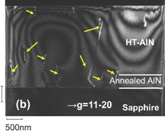
Fig. 6. Dark-field cross-sectional TEM images of AlN with tHT = 2 µm grown at THT = 1450 °C on annealed AlN buffer layers (TBuf = 1200 °C, tBuf = 300 nm, TAn = 1700 °C) under the two-beam condition with (a) g = 0002 and (b)  . The thickness of the TEM specimen is about 100 nm. No type-a+c or type-c dislocations can be observed in (a). Type-a dislocations can be observed in (b), and their density is estimated to be 5 × 108 cm−2.
Download figure:
Standard image High-resolution image
In conclusion, we have clarified the effects of annealing in a carbon-saturated N2–CO mixture on AlN buffer layers grown on sapphire substrates. The morphology and RMS value of the AlN buffer layer surface markedly changed after annealing at temperatures above 1500 °C. The FWHMs of the ( )-plane XRCs for the AlN buffer layers significantly decreased with increasing annealing temperature up to 1700 °C. However, for the AlN buffer layers after annealing at 1750 °C, the FWHMs of the (0002)- and (
 )-plane XRCs increased and the surface was rough.
A high-quality AlN layer was successfully grown on the annealed AlN buffer layer on a sapphire substrate by MOVPE. The FWHMs of the (0002)- and ( )-plane XRCs were 16 and 154 arcsec, respectively. Most of the threading dislocations were of type-a, and their density was 4.7 × 108 cm−2.
Acknowledgments
This work was partially supported by the Akasaki Research Center of Nagoya University, Grants-in-Aid for Specially Promoted Research (No. 25000011) and Scientific Research (B) (No. 15H03556) from the Ministry of Education, Culture, Sports, Science and Technology (MEXT), the Inter-University Cooperative Research Program of the Institute for Materials Research, Tohoku University, Nanotechnology Platform Japan, Kyushu University, and Fundamental Research Grant Scheme (FRGS/2/2013/SG06/UTM/01/2) from Ministry of Education (MoE), Malaysia. This work was also funded by the Cabinet Office, Government of Japan, through its Funding Program for Next Generation World-Leading Researchers.