Abstract
Molecular orientation in organic light-emitting diodes (OLEDs) is now regarded as an important factor that affects device efficiency. However, methods to quantitatively estimate the degree of molecular orientation in OLEDs are currently limited, and they require constructing a model of an optical structure. Here, we propose a simple model-free method to estimate the orientation order parameters (S) of molecules in amorphous OLED films from their absorption spectra using the randomization of molecular orientation induced by heating. This method is used to quantitatively estimate the S values of vacuum-deposited and spin-coated films and clearly demonstrate the random orientation in the latter.
Export citation and abstract BibTeX RIS

Content from this work may be used under the terms of the Creative Commons Attribution 4.0 license. Any further distribution of this work must maintain attribution to the author(s) and the title of the work, journal citation and DOI.
This article was made open access on 10 September 2015
As the performance of organic light-emitting diodes (OLEDs) has increased, the importance of fundamentally understanding their amorphous films to further improve their efficiency and stability has been recognized. In particular, molecular orientation in amorphous OLED films has recently been investigated extensively because its effects on device performance are considerable, especially when discussing high OLED performance close to the theoretical limit.1–5) The degree of molecular orientation in OLED films is now regarded as one of the main factors that affect film properties and device efficiency.
However, because amorphous organic films do not have a distinct long-range periodic structure, their higher-order structures cannot be readily analyzed by X-ray diffraction measurements. Methods to quantitatively estimate the degree of molecular orientation in amorphous organic films are currently limited, with two methods being commonly used. The first is variable angle spectroscopic ellipsometry (VASE),1,6,7) which can determine the optical constants and their anisotropies of thin films by fitting simulated ellipsometric parameters to experimental ones using a modeled structure of optical constants and film thickness in a sample. From the ratio of the peak amplitudes of the extinction coefficients in the horizontal and vertical directions, we can quantitatively estimate the orientation order parameter (S) of transition dipole moments of molecules in a film.1,7) Although this method is very useful, it also has some drawbacks. Because the result of VASE analysis depends on the initial model of the optical structure of a sample to some extent, it is necessary to carefully construct the initial model that can be regarded as "most probable" one and sufficiently confirm that the result is unique and not contradictory to any physical conditions or other experimental results, such as absorption spectra. From this aspect, VASE is an indirect method to estimate the degree of molecular orientation. It should also be noted that VASE analysis is not sufficiently sensitive to the anisotropies in a very thin sample film. For example, quantitative estimations of S in a film with a thickness of several tens of nanometers can have a large error and sometimes result in an incorrect artifact. In addition, because each model has many fitting parameters including the anisotropy of extinction coefficients, the estimations of S are affected by errors included in the initial optical model. Experimental systems for VASE are also expensive, which is another disadvantage of this approach.
The second method commonly used to measure molecular orientation in amorphous organic films is analysis of the angular distribution of the photoluminescence (PL) from a sample film. This can be applied to materials with high fluorescent or phosphorescent PL efficiency to estimate the degree of orientation of the transition dipole moments for emission.2,4,8) However, this method also needs optical simulations and fitting procedures based on an ideal optical model including optical constants and the thicknesses of films in the sample. Thus, similar to VASE, this is an indirect method to estimate the degree of molecular orientation in films. The errors of the optical constants and their anisotropies affect the results. Although the experimental system for such PL measurements is not as expensive as that for VASE, it is necessary to carefully adjust the optical alignment in the system to avoid possible errors.
In this paper, we propose a simple model-free method to estimate the S values of amorphous OLED films from their absorption spectra using their tendency for molecular orientation to be randomized via a transition induced by heating. Using this method, we quantitatively compare the S values of vacuum-deposited and spin-coated films of some amorphous OLED materials. The results clearly demonstrate that the absolute S values of the former are generally higher than those of the latter, which are nearly zero.
Figure 1 shows the chemical structures of the main OLED materials used in this study including N,N'-diphenyl-N,N'-di(m-tolyl)benzidine (TPD), N,N'-di(1-naphthyl)-N,N'-diphenylbenzidine (α-NPD), 4,4',4''-tris[2-naphthyl(phenyl)amino]triphenylamine (2-TNATA), N4,N4'-(biphenyl-4,4'-diyl)bis(N4,N4',N4'-triphenylbiphenyl-4,4'-diamine) (TPT1), and 2,7-bis(9,9-spirobifluoren-2-yl)-9,9-spirobifluorene (TSBF), which have glass transition temperatures (Tg) of 60, 96, 110, 144, and 231 °C, respectively.9–12) For each material, we fabricated vacuum-deposited films with thicknesses of 20, 50, and 100 nm on fused silica and Si(100) substrates at a deposition rate of 2 Å/s under a vacuum of <1 × 10⁻³ Pa. Spin-coated films were also fabricated on the same types of substrates using solutions of each material in chloroform (15 mg/mL) at spin speeds of 1000, 3000, 5000, and 7000 rpm, followed by mild baking under nitrogen atmosphere for 30 min on a hot plate at a temperature lower than Tg: 50 °C for TPD and 80 °C for the other materials. We measured the absorption spectra of all the sample films on fused silica substrates using a spectrophotometer (Shimadzu UV2450). The thicknesses of the organic films on Si(100) substrates were determined by VASE using a variable angle spectroscopic ellipsometer (J. A. Woollam M-2000U) as described elsewhere.7) In this VASE analysis, we used a very simple model with only four fitting parameters based on the Cauchy model with an additional parameter representing birefringence for uniqueness and accuracy, and applied it only to the transparent spectral region of 600–1000 nm. After the above measurements, all the samples were annealed under nitrogen atmosphere for 30 min on a hot plate at a temperature sufficiently higher than Tg: 80, 120, 130, 170, and 250 °C, for TPD, α-NPD, 2-TNATA, TPT1, and TSBF, respectively. The sample films were naturally cooled to room temperature, and then the absorption spectra of all the sample films on fused silica substrates were measured again. In addition, we analyzed the optical anisotropies of the 100-nm-thick vacuum-deposited sample films on Si(100) substrates by VASE in the spectral region of 245–1000 nm using a general oscillator model with Gaussian-shaped bands.7)
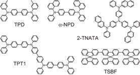
Fig. 1. Chemical structures of the main OLED materials used in this study.
Download figure:
Standard image High-resolution imageFigure 2 shows the results of the VASE analysis of the 100-nm-thick vacuum-deposited films after annealing. The refractive indices and extinction coefficients of all of these films were isotropic. This result confirms that the molecular orientation in these amorphous organic films becomes random via a transition upon heating to a temperature sufficiently higher than Tg, as reported previously.13–16)

Fig. 2. Anisotropic refractive indices and extinction coefficients of the 100-nm-thick vacuum-deposited films after annealing. The red solid and dashed lines show the refractive indices in the horizontal and vertical directions (no and ne), respectively. The blue solid and dashed lines show the extinction coefficients in the horizontal and vertical directions (ko and ke), respectively.
Download figure:
Standard image High-resolution imageThe absorption spectra of all the sample films on fused silica substrates before and after annealing are shown in Fig. 3. There are notable differences between the changes in the absorption spectra of the vacuum-deposited and spin-coated films before and after annealing. Except for the TPD films, the absorbances of the vacuum-deposited films decreased markedly after annealing. These decreases in absorbance originate from the change in molecular orientation before and after annealing. In as-prepared vacuum-deposited OLED films, molecules are generally oriented depending on their molecular shape; the larger the anisotropy of a molecular shape, the higher the degree of horizontal molecular orientation.1,7) In addition, the correlation between Tg and molecular orientation in vacuum-deposited amorphous films has been reported.15) Thus, most of the materials used in this study adopt horizontal molecular orientation in as-prepared vacuum-deposited films, whereas the molecular orientation becomes random after annealing, as shown in Fig. 2. Because the electric field of the normal incident light of the spectrophotometer is horizontal to the substrate surface, the absorbance is proportional to 〈sin2 θ〉, where 〈...〉 indicates the ensemble average, and θ is the angle between the transition dipole moment for the light absorption of a molecule and the surface normal. Thus, the decrease in absorbance reflects the randomization of molecular orientation.17) In contrast to the considerable changes in the absorbances of the vacuum-deposited films, those of the spin-coated films were nearly unchanged after annealing. This result directly demonstrates that the molecular orientations in the as-prepared spin-coated films are nearly random similarly to those in the annealed spin-coated films.

Fig. 3. Absorption spectra of the vacuum-deposited and spin-coated films before and after annealing. The solid lines show the spectra of the as-prepared films before annealing, and the dashed lines show those after annealing.
Download figure:
Standard image High-resolution imageIn general, S is defined by the following equation;
which has been widely used to quantify the degree of molecular orientation for liquid crystals and polymers18,19) and also recently been applied to amorphous small-molecule organic semiconductor films.1,7) For a film, S = −0.5 if the transition dipole moments are completely horizontal to the substrate surface, S = 0 if they are randomly oriented, and S = 1 if they are completely vertical. The absorbance of an as-prepared film, A, and that of the film after annealing with completely isotropic (random) molecular orientation, Aiso, can be respectively represented as follows;


where A0 is the hypothetical absorbance when the transition dipole moments of all the molecules are completely parallel to the electric field of the incident light. From Eqs. (1)–(3), we can obtain the following simple relationship between S and the absorbances;
[The details of the derivation of Eqs. (2)–(4) are represented in the online supplementary data at http://stacks.iop.org/APEX/8/096601/mmedia.] We determined the values of A and Aiso using the long-wavelength absorbance peaks except for TPT1. The values of A and Aiso for TPT1 were determined at 360 nm because the shoulder around this wavelength is assigned to the lowest-energy electronic transition. The transition dipole moments corresponding to these absorptions are nearly along the long molecular axis for TPD, α-NPD, TPT1, and TSBF, and nearly parallel to the molecular plane of the central triphenylamine for 2-TNATA. (The calculated results are shown in the online supplementary data at http://stacks.iop.org/APEX/8/096601/mmedia.) The originality of our method is in the use of randomly oriented films fabricated by annealing as references for the quantitative estimation of S of amorphous films. The irreversible randomization of molecular orientation by annealing is a unique nature of amorphous organic films, and its effective use for the simple quantitative estimation of S of OLED films has never been reported.
Table I shows the S values estimated using Eq. (1), revealing quantitative differences in S between the vacuum-deposited and spin-coated films. The S values of the spin-coated films are nearly zero, whereas the vacuum-deposited films have larger absolute S values. This random orientation of spin-coated films is generally seen for most small-molecule OLED materials.16) In the spin-coated films, only the TSBF films have S values that slightly deviate from zero, indicating the possibility that oligomers can be horizontally oriented even in spin-coated films as with polymers.20–22) In Table I, we also show the S values estimated by VASE using the 100-nm-thick as-deposited vacuum-deposited films on Si(100) substrates. The S values estimated by our new method and VASE are within small differences. (The detailed comparison between the two methods is presented in the online supplementary data at http://stacks.iop.org/APEX/8/096601/mmedia.) It should be noted that the new method can be applied to films with a thickness of just a few tens of nanometers. Because the estimation of S in such thin films by VASE sometimes results in an incorrect artifact, the direct estimation of S through our simple method is very useful.
Table I. Orientation order parameters of vacuum-deposited and spin-coated films estimated by the method in this study. The values estimated by VASE are also shown. The values in parentheses indicate the film thicknesses in the unit of nm determined by VASE.
| Material | Vacuum-deposited | Spin-coated | ||||||
|---|---|---|---|---|---|---|---|---|
| 20 nm | 50 nm | 100 nm | VASEa) 100 nm | 7000 rpm | 5000 rpm | 3000 rpm | 1000 rpm | |
| TPD | −0.06 | −0.04 | −0.02 | −0.04 | −0.01 (47) | 0.00 (53) | 0.00 (68) | −0.01 (116) |
| α-NPD | −0.15 | −0.16 | −0.18 | −0.20 | −0.01 (46) | −0.01 (51) | 0.00 (67) | 0.00 (114) |
| 2-TNATAb) | −0.23 | −0.24 | −0.29 | −0.24 | −0.01 (46) | −0.01 (51) | −0.01 (63) | −0.01 (118) |
| TPT1 | −0.25 | −0.24 | −0.24 | −0.24 | −0.02 (41) | −0.01 (47) | −0.01 (60) | −0.01 (110) |
| TSBF | −0.28 | −0.31 | −0.32 | −0.35 | −0.05 (46) | −0.03 (55) | −0.05 (69) | −0.03 (120) |
a) The estimation by VASE was performed using films with a thickness of 100 nm on a Si(100) substrate.
b) The estimation was performed using the absorbance at 360 nm for all 2-TNATA films because the peak wavelength for the lowest-energy electronic transition was unclear.
Our method can also be applied to doped films. Even in vacuum-deposited doped films fabricated by codeposition, molecules are oriented as in neat films.1,7,8) Figure 4 shows the change in the absorption spectrum of a vacuum-deposited DSA-Ph (20 wt %):TPD film with a thickness of 100 nm, where DSA-Ph is 1,4-bis[4-(diphenylamino)styryl]benzene7) (its chemical structure is illustrated in the inset). The absorption spectrum of the as-prepared film and that after annealing at 75 °C for 30 min are shown. Although Tg of DSA-Ph (87 °C15)) is higher than this annealing temperature, we found that the molecular orientation of DSA-Ph became random in the doped film upon the transition of TPD, whose Tg is 60 °C. This absorption spectrum did not change after further annealing at 100 °C for 30 min, indicating that the orientation of guest DSA-Ph molecules became random by the transition of TPD in the first annealing process at 75 °C. The S value of DSA-Ph in the doped film before annealing was estimated as −0.28.

Fig. 4. Absorption spectra of vacuum-deposited DSA-Ph (20 wt %):TPD films before and after annealing (red solid and dashed lines, respectively). The absorption spectra of 100-nm-thick vacuum-deposited DSA-Ph (blue) and TPD (gray) neat films are also shown for reference.
Download figure:
Standard image High-resolution image
Finally, we also mention some drawbacks of our new method. First, it cannot be applied to OLED materials that tend to crystallize upon heating. We tried to estimate the S values of films of tris(8-hydroxyquinoline)aluminum (Alq3) and 4,4'-bis(N-carbazole)biphenyl (CBP), but it was not possible to fabricate their isotropic amorphous films by annealing because of their crystallization followed by the emergence of haze. Second, the estimation of S using Eq. (1) is based on the assumption that the molecular orientation in a film after annealing at a temperature over Tg is completely random. We think that this assumption is valid for most of the OLED materials that do not crystallize after transition, and we confirmed it for the materials used in this study, as shown in Fig. 2, but there might be exceptions. Third, the absorption spectra of thin films are generally affected by film thickness. Because of the interference effect caused by multiple reflections between the air/organic and organic/substrate interfaces, spectral shapes and peak wavelengths of absorption seem to depend on film thickness to some degree.16) For example, the fluctuation of the baselines and their dependence on film thickness can be seen in the spectral region of 400–500 nm in Fig. 3. The interference effect sometimes causes a slight shift of peak wavelengths or an over/underestimation of absorbance, which may lead to a small error in the estimation of S. However, despite these drawbacks, our method has many advantages including (1) simplicity, (2) model-free estimation, (3) inexpensive experimental system, and (4) applicability to very thin films. Therefore, we believe that this approach will become one of the standard methods to estimate S of amorphous OLED films. We also intend to apply our simple method to IR absorption in the future to quantitatively analyze the orientation of functional groups of OLED materials.
In summary, we propose a simple new method to estimate S of amorphous films used for OLEDs from their absorption spectra using the tendency of molecular orientation to be randomized via a transition induced by heating. Using this method, we demonstrated the quantitatively distinct difference between molecular orientations in vacuum-deposited and spin-coated OLED films. We found that the molecular orientation in spin-coated films is nearly random (S ∼ 0). Because our method is simple, model-free, inexpensive, and applicable to films with a small thickness of just a few tens of nanometers, it is promising as a standard method to estimate S of OLED films.
Acknowledgments
This work was financially supported in part by KAKENHI (Grant Number 25708038) from the Japan Society for the Promotion of Science (JSPS). The quantum chemical calculations were performed using computers in the Research Center for Computational Science, Okazaki, Japan.