

Abstract
We investigate photo-induced lattice strains of a monoclinic VTe2 thin flake using ultrafast electron diffraction. After photoexcitation by a 190 fs pulse, we observe diffraction intensity oscillations with periods of 35 and 75 ps, which indicate coherent acoustic phonons of two distinct branches. The oscillations of  and
and  diffraction intensities have opposite signs, indicating the change of the diffraction angle due to the shear strain. By numerically simulating these diffraction intensities as a function of the monoclinic angle, we evaluate the amplitude of the photo-induced shear strain.
Export citation and abstract BibTeX RIS
Ultrafast photogeneration of coherent acoustic phonons has attracted significant interest owing to its potential application for ultrasonic devices and optomechanics. Since the 1980s, photogeneration and propagation of coherent longitudinal acoustic (LA) phonons have been intensively studied1–3) in simple metals, semiconductors, and other materials, by employing ultrafast optical pump–probe measurements. When a femtosecond laser pulse is irradiated onto solids, impulsive strains are generated at the surface predominantly due to the thermoelasticity4–7) and deformation potential,1,3,8–10) and propagate through the sample in the form of pulsed strains. In the case of thin samples, they are observed as echo signals at the surface, owing to the reflections at the back surfaces. When the sample thickness d is comparable with or smaller than the optical penetration depth, the coherent acoustic phonon is manifested as a standing wave, which can be regarded as an acoustic breathing-type oscillation of the thin film.11) The time period T of the fundamental breathing oscillation is T = 2d/v, where v is the sound velocity along the thickness direction.
The ultrafast pump–probe technique is recently employed in electron diffraction measurements [ultrafast electron diffraction (UED)].12–16) It enables quantitative evaluation of collective atomic displacement in short timescales such as femtoseconds and picoseconds.17–20) The coherent LA phonons have been also directly identified by UED in some thin-film metals and semiconductors.11,21–25) In these studies, the characteristic oscillations of the electron diffraction intensity were detected as a function of the delay time. It has been discussed in terms of changes in the diffraction efficiency reflecting the deviations from the ideal Bragg condition. A significant change in the diffraction intensity is expected from a small zone-axis tilt, which can be caused by the photo-induced anisotropic lattice expansions and/or morphological effects (surface bulging).11,25) This makes the UED a very sensitive probe for detection of coherent acoustic phonons. Nevertheless, the photogeneration of coherent transverse acoustic (TA) phonons is challenging; a very few related studies have been reported.17,26) For further development of photoacoustic functions, new materials that can effectively transform photons into large-amplitude TA phonons are required.4)
In this study, we focus on VTe2, which exhibits a trigonal-to-monoclinic structural phase transition at 480 K.27) As the low-temperature monoclinic crystal structure is characterized by a strong shear distortion coupled to the zigzag chains of V–V bonds, unusual lattice dynamics can be expected by the instantaneous photoexcitation. By utilizing UED, we successfully observe two types of oscillations in the diffraction intensities, indicating the propagation of coherent acoustic phonons of two distinct branches accompanying the shear strains. We further perform numerical simulations to evaluate the amplitude of the coherent shear strain wave in VTe2.
Figure 1(a) shows the experimental setup of the UED system.28) It consists of a femtosecond laser (Light Conversion PHAROS) and ultra-high-vacuum electron diffraction system with a photocathode (APCO ARH-30). The repetition rate of the laser is in the range of 1 to 200 kHz. The fundamental laser beam (1030 nm, 190 fs) is split into two branches, pump and probe, by a polarized beam splitter (BS). The probe line passes through two β-Ba2B2O4 (BBO) crystals for fourth-harmonic generation. The frequency-quadrupled 257-nm laser pulse is focused on a photocathode made of a 10-nm-thick gold film evaporated on the quartz window. The electron packet for the probe is then generated through photoemission. The electron packets are accelerated to 60 keV and used to obtain the electron diffraction image. The rest of the laser beam is used to excite the sample with a controlled time delay relative to the electron packet. The diameters of the pump laser and probe electron beams are set to 330 and 120 µm at the sample, respectively, which ensure homogeneous photoexcitation in the probing area. The time resolution of the UED measurements was set to 5 ps to obtain data with a high signal-to-noise ratio. All UED measurements for VTe2 were performed at room temperature (300 K), with a repetition rate of 10 kHz.
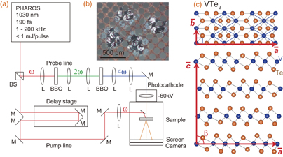
Fig. 1. (a) Schematic of the experimental setup for UED. BS, L, and M denote the beam splitter, lens, and mirror, respectively. (b) Thin flakes of VTe2 mounted on a Cu grid used for the UED measurements. (c) Crystal structure of VTe2. The red arrows represent the nonconventional monoclinic lattice vectors used to describe the Miller indices in this study.
Download figure:
Standard image High-resolution imageA high-quality VTe2 single-crystal was used for the UED measurements. We prepared thin flakes of VTe2 by an ultramicrotome. The target value of the thickness was 50 nm. The thin flakes were placed on a copper grid, as shown in Fig. 1(b). The relative distribution of the thickness is evaluated to be within ±10% by the log-ratio technique of electron energy-loss spectroscopy.29) At room temperature, VTe2 has a monoclinic structure (C2/m), as shown in Fig. 1(c).27) We use nonconventional lattice vectors,  ,
,  , and
, and  to describe the Miller indices of the diffraction spots. The angle between
  and
and  is 90°, while that between
  and
and  is 90.37° (monoclinic angle β). VTe2 consists of layers weakly stacked along the
  -axis by van der Waals coupling. Each layer is formed by edge-sharing VTe6 octahedra, which are strongly distorted from trigonal symmetry owing to the zigzag chain structures of V bonds along the
  -axis. Therefore, the crystal structure of VTe2 indicates the strong one-dimensional character. In this study, the incident electron beam was fixed perpendicular to the layer, i.e., perpendicular to both
  and
and  .
.
First-principles calculations of the elastic constant of VTe2 were performed based on the van der Waals density functional theory30–32) using the pseudopotential method in conjunction with the generalized gradient approximation,33) as implemented in the VASP software package.34) The wave functions were expanded in the plane-wave basis with a cut-off energy of 700 eV to ensure good convergence of the stress and elastic tensor. Brillouin zone integration was performed on a 1 × 8 × 2 Monkhorst–Pack k-point mesh.35) All free degrees within the space group, C2/m, were relaxed with a force convergence criterion of 0.001 eV/Å. The optimized lattice parameters deviate less than 1% from the experimental values.
We present the static electron diffraction of VTe2 at 300 K. The electron diffraction image in Fig. 2(a) shows two-fold symmetry, as expected from the monoclinic crystal structure with the one-dimensional V chains. The electron diffraction image includes significantly more diffraction spots than those predicted by the simple numerical simulations. In general, the diffraction intensity detected by electron diffraction measurements is determined by the interception of the Ewald sphere with the diffraction spots in the reciprocal space. In reality, the diffraction spots have elongated widths mainly due to the thinness and roughness of the samples, which can lead to the increase in the overlap between the diffraction spots and Ewald sphere. In the present case, the thickness of the sample (50 nm) is sufficiently large, compared to the lattice constant, and thus cannot explain the presence of the additional peaks including the  and
and  spots in Fig. 2(a). Therefore, this indicates the imperfectness of the thin-flake samples strongly affecting the diffraction.

Fig. 2. (a) Static electron diffraction patterns of VTe2 recorded at room temperature. (b–f) Simulated diffraction patterns of VTe2 including Gaussian-type angle broadenings with σ = 1, 3, 5, 7, and 9°, respectively.
Download figure:
Standard image High-resolution imageWe compare the experimentally obtained electron diffraction image with the numerical simulations in Figs. 2(b)–2(f). In the simulation, we introduce Gaussian-type broadening of the diffraction angle with a standard deviation of σ, representing the distribution of the  -axis orientation (
 ) due to the undulation of the thin flake. The structural and Debye–Waller factors are calculated using atomic scattering factors36) and crystal structure parameters of VTe2,27) based on the kinematic diffraction theory. We also assume a Gaussian-type distribution of the diffraction intensity along the radial directions in the reciprocal space with a standard deviation of 0.06 Å−1, in order to reasonably reproduce the experimentally obtained electron diffraction pattern. For σ = 1°, as shown in Fig. 2(b), the number of diffraction spots is still very small, compared to that in the experiment [Fig. 2(a)]. However, with the increase in σ, additional spots gradually appear and the simulated electron diffraction pattern becomes similar to the experimental pattern at σ of approximately 3–5°. This angle broadening should reflect the wrinkles of the thin flake, as shown in Fig. 1(b).
Further, we show the time-resolved behavior of the electron diffraction intensities after the femtosecond photoexcitation. As shown in Fig. 3(a), the diffraction intensity normalized at the negative delay time (I/I0) of  and
and  spots exhibit a 15% decrease within 5 ps. This indicates a quick photo-induced structural change, as the increase in the lattice temperature up to 310 K, estimated from the lattice heat capacity (Dulong–Petit law) and experimental value of the absorption rate (70%), is insufficient to explain the observed decrease in the diffraction intensity. It is worth noting that this temperature (∼310 K) is significantly below the structural-phase-transition temperature (480 K). The reductions in the
  and
and  diffraction intensities expected by the Debye–Waller effect due to the temperature change from 300 to 310 K should be smaller than 0.5%, assuming that the square atomic displacements reported in Ref. 27 are proportional to the temperature. This should be applicable for VTe2 considering that its Debye temperature is significantly lower than room temperature.37) Further, we observed the oscillatory responses in a longer time scale for both diffraction spots. The I/I0 curves are reproduced by fitting including an exponential function (1 − e−t/τ) with a time constant of τ = 5 ps and oscillatory component with a period of 75 ± 6 ps, represented by the black solid curves in Fig. 3(a). On the other hand, for the
  and
and  spots, an overlap of two oscillatory components with periods of 75 ± 6 and 35 ± 4 ps is detected, represented by the solid green curves in Fig. 3(b). It is worth noting that the effect of the Debye–Waller factor estimated for the
  and
and  spots leads to reductions in the intensities smaller than 0.5%.

Fig. 3. Time dependences of the (a)  and
and  and (b)
  and
and  diffraction intensities. The black curves in (a) and (b) are the fitting curves. The dashed and solid green curves represent the two oscillatory components of
  obtained from the fitting curves. (c) and (d) Simulated diffraction intensity profiles for σ = 3° on the planes indicated by the blue and red rectangles on the right side of each image, respectively. The black arrows indicate the direction of the reciprocal lattice rotation when the monoclinic angle β is decreased. (e) Time dependence of Δβ converted from the experimental data in (b), for σ values from 1 to 9°. The pink curves in (c), (d), and (g) represent the cross section of the Ewald sphere. (f) Red curves show the I/I0 of
  and
and  calculated as a function of β for the case of σ = 3°. The black curve represents the ratio f of the
  and
and  diffraction intensities. (g) Magnified profiles around
  and
and  shown in (d).
Download figure:
Standard image High-resolution image
The two oscillation periods of 35 and 75 ps imply the presence of two coherent acoustic phonons of distinct branches. In order to investigate this interpretation, we calculated the elastic constant C for VTe2. The sound velocities of acoustic phonons propagating along the z-axis are calculated to be 2400 ± 450 and 1200 ± 240 m/s, for predominantly longitudinal acoustic (LA') and transverse acoustic (TA') branches, respectively. It is worth noting that the LA and TA components are slightly mixed in VTe2 owing to the monoclinic structure. These values of the sound velocities v agree well with the observed oscillation periods T, considering the standing-wave of the acoustic strain waves with T = 2d/v formed in the thin flake with a thickness of d = 50 nm.
The oscillation component of the  diffraction intensity has the opposite sign to that of the
  spot, as shown in Fig. 3(b). As discussed in the previous UED study,17) such antisymmetric behavior of hk0 and
  diffraction intensities can be explained only by the change in the diffraction angle, which modifies the interception of the Ewald sphere with the diffraction spots. In the present case, we can consider the change in the monoclinic angle β, which leads to a tilt of the 1 0 0 zone axis. We simulate the diffraction intensity profiles in the reciprocal plane spanned by the
  and
and  directions, as shown in Fig. 3(d). The diffraction spots are elongated along the tangential direction owing to the angle broadening parameter of σ = 3°, set as a representative value. As we assume that the monoclinic angle β (90.37° for room-temperature VTe2) should change by the photoexcitation, the orientation of the
  axis should change correspondingly, and the diffraction rods are expected to move along the direction indicated by the black arrows in Fig. 3(d). In this case, the changes in the
  and
and  diffraction intensities should be opposite in sign, as both centers of the rods are located slightly below the Ewald sphere [Fig. 3(g)]. In contrast, the
  and
and  spots are located at opposite sides of the Ewald sphere [Fig. 3(c)], which leads to the same signs of the diffraction intensity changes when β is modified. This interpretation seemingly shows good agreement with the experimental observations in Figs. 3(a) and 3(b).
Based on this interpretation, we evaluate the change in β, Δβ, in comparison with the experimentally obtained I/I0 curves. Figure 3(f) shows the normalized  and
and  diffraction intensities simulated as a function of β for the case of σ = 3°. The other lattice constants are fixed in the simulation. The black curve represents the ratio of the
  and
and  normalized diffraction intensities,

Using the f–β relation in Fig. 3(f), we convert the experimental data in Fig. 3(b) to Δβ, for the σ values in the range of 1 to 9° [Fig. 3(e)]. In the case of σ = 3°, near the lower limit, the observed oscillatory intensities correspond to the amplitude of Δβ ∼ 0.5°. The coherent shear strain wave with Δβ ∼ 0.5° generated by the optical pulse of 0.13 mJ/cm2 is significantly larger than that reported in normal semiconductors such as Si, where the observed change in the diffraction angle is smaller than 0.1° even by the significantly stronger optical pulse excitation of 2 mJ/cm2.17) The quantitative evaluation of Δβ depends on the accuracy of σ. We show that the characteristic monoclinic crystal structure of VTe2 can be a suitable platform for generation of a large-amplitude coherent shear strain wave. The microscopic mechanism of the coherent acoustic phonon generation should be further investigated.
In conclusion, we investigated the ultrafast lattice dynamics of 50-nm-thick thin flakes of monoclinic VTe2. We observed the oscillations in the  and
and  diffraction intensities with the periods of 35 and 75 ps generated by the photoexcitation. By comparison with the first-principle calculations of the sound velocities, these oscillations were assigned as the standing waves of the coherent LA' and TA' phonons. We analyzed the diffraction intensity profiles of the real thin-flake sample, and evaluated the amplitude of the shear strain wave by the numerical simulations of the monoclinic angle.
Acknowledgments
This research was partly supported by the Photon Frontier Network Program of the MEXT and Research Hub for Advanced Nano Characterization, University of Tokyo, supported by the MEXT, Japan. A. Nakamura acknowledges the support by the Advanced Leading Graduate Course for Photon Science (ALPS) at the University of Tokyo.