
Abstract
Time-resolved electric-field-induced sum-frequency generation (EFI-SFG) spectroscopy was employed to study the charge behavior of multilayer organic light-emitting diodes (OLEDs). Through application of the square wave pulse bias to the OLEDs, compensation for the polarization charges in the electron transport layer and the generation of 4,4'-bis[N-(1-naphthyl-N-phenylamino)-biphenyl] (α-NPD) cations were observed. When the pulse voltage was turned off, the α-NPD cations immediately disappeared, confirming that charge recombination occurs at the interfaces. We therefore concluded that time-resolved EFI-SFG is useful for directly probing the carrier behavior in OLEDs in addition to identifying the origin of the charge carriers present in OLEDs.
Export citation and abstract BibTeX RIS

Content from this work may be used under the terms of the Creative Commons Attribution 4.0 license. Any further distribution of this work must maintain attribution to the author(s) and the title of the work, journal citation and DOI.
Organic light-emitting diodes (OLEDs) have attracted significant attention as next-generation full-color display devices, and are beginning to be widely used in mobile phones and OLED television sets.1,2) OLEDs also exhibit potential for providing energy savings in a range of applications, including lighting and flexible panel displays. Indeed, since the development of high-efficiency double-layer OLEDs, the emission efficiency and device reliability of OLEDs have greatly improved.3) In the context of their structure, current highly efficient OLEDs have a characteristic multilayered structure, where each organic layer has a different function.4,5) More specifically, the interfacial structures and properties of the OLEDs in relation to charge separation, transfer, and accumulation at the interfaces and ultrathin organic layers are of extreme importance in determining their charge carrier behavior, as both the charge transport and the concentrations of charge carriers in organic thin-film layers are directly associated with the functions of multilayer OLEDs. Furthermore, the formation and decay of electronically excited states, in addition to the generation and recombination of carriers within the organic layers and interfaces, are essential processes in OLEDs. Therefore, examination of the carrier dynamics in multilayer OLEDs under operation is of particular importance. The time-of-flight method is one of the useful techniques of probing carrier motion in organic materials,6) but it is difficult to apply this technique to real multilayer devices. Transient electroluminescent measurements are also helpful for exploring carrier behaviors;7) however, it cannot provide information on carrier behavior until the electroluminescence is generated. Although investigation of the charges present in such organic devices can be challenging, it is possible by monitoring the electric field created by the injected charges through electric-field-induced second harmonic generation (EFI-SHG) or sum-frequency generation (SFG).8–10) For example, Iwamoto and coworkers pioneered the use of EFI-SHG to study charge accumulation and field distribution in organic devices.11–13) Although EFI-SHG is an effective technique for obtaining direct information regarding the charge transport phenomenon in organic devices, this technique can also be extended to more complex organic devices using electric-field-induced doubly resonant SFG. In this context, we have recently reported our observations of the vibrational spectra of the component layers in multilayer OLEDs with a drive voltage application using direct current (DC) electric-field-induced sum-frequency generation (EFI-SFG) spectroscopy.14) Through measurement of the EFI-SFG spectra under double resonance conditions, molecular selectivity is greatly enhanced,15,16) and it becomes possible to extract information regarding the specific organic layer of interest. This technique was further applied to both pristine and aged OLEDs, and we were successful in determining the behavior of each component material of the multilayer OLEDs through identification of the vibrational spectra of the component molecules. From the SFG observations, we detected changes in the molecular orientation of the commonly used electron transport material tris(8-hydroxyquinoline)aluminum (Alq3) due to the continuous driving stress.17)
Thus, we herein report the direct observation of the charge injection, transport, and accumulation behavior in multilayer OLED devices by time-resolved EFI-SFG. The use of this technique also allows us to determine that charge carrier generation and recombination at the organic interfaces varied with time in response to the applied pulse bias voltage. These observations therefore enable us to understand the real-time charge carrier behavior in various multilayer OLEDs using nondestructive methods.
The structure of the OLED devices employed in this study was based on that of a conventional multilayer OLED,4,5,14) as illustrated in Fig. 1. The device was prepared using 1,4,5,8,9,11-hexaazatriphenylene hexacarbonitrile (HAT-CN) as the hole injection layer, 4,4'-bis[N-(1-naphthyl-N-phenylamino)-biphenyl] (α-NPD) as the hole transport layer, 4,4'-N,N'-dicarbazole-biphenyl (CBP) doped with 6 wt % tris(2-phenylpyridinato)iridium(III) [Ir(ppy)3] as the phosphorescent emission layer, aluminum(III) bis(2-methyl-8-quninolinato)-4-phenylphenolate (BAlq) as the hole blocking layer, Alq3 as the electron transport layer, and an indium zinc oxide (IZO) electrode, a LiF anode, and an Al cathode to give the following device structure: IZO (150 nm)/HAT-CN (60 nm)/α-NPD (20 nm)/6 wt % Ir(ppy)3/CBP (30 nm)/BAlq (10 nm)/Alq3 (30 nm)/LiF (1.6 nm)/Al (150 nm). All devices were prepared on a transparent CaF2 substrate to give an emission area of 2 × 2 mm2. A sealed glass cap containing a desiccant protected the organic layers from the permeation of ambient moisture.
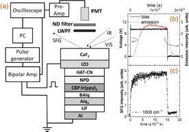
Fig. 1. (a) Device structure of the OLEDs employed herein and the optical and electrical arrangements for the time-resolved EFI-SFG measurements. (b) Emission response of OLEDs upon application of a square-wave pulse bias. (c) SFG response at 1600 cm−1 upon application of a pulse bias voltage.
Download figure:
Standard image High-resolution imageThe basic SFG system employed herein was described in our previous paper.15) All reported SFG spectra were obtained using a PPP polarization combination, in which infrared (IR), visible, and SFG light were polarized in the plane of incidence, and the incident angles of the visible and IR beams were 70 and 50° from the surface normal, respectively. The prepared multilayer OLEDs were operated with the application of a pulse square wave voltage using a pulse delay generator (Stanford Research Systems DG535) and a high-speed bipolar amplifier (NF HSA4101). Emission from the OLEDs was detected using a photomultiplier (Hamamatsu H10721) equipped with a high-speed preamplifier (Hamamatsu C9999), and was stored by an oscilloscope (Tektronix TDS-2022C). The injected current was monitored using a current probe (Tektronix TCP2020) and again stored by an oscilloscope.
The emission response of the OLEDs and the EFI-SFG intensity response at 1600 cm−1 under application of the square-wave bias voltage of 10 V are shown in Fig. 1(b), where the pulse width is set to 15 µs. In addition, the SFG signal intensity at 1600 cm−1 according to the applied square-wave bias voltage is shown in Fig. 1(c). As indicated, emission from the OLEDs begins following a charge injection of ∼1 µs. Furthermore, as shown in Fig. 1(c), the SFG signal intensity varies upon the application of a pulse voltage to the OLEDs.
The time-resolved EFI-SFG spectra of the OLEDs taken at the visible excitation wavelength of 460 nm are shown in Fig. 2. Prior to application of the voltage, the obtained SFG spectrum was comparable to the previously reported SFG spectrum of the OLED device in the absence of a bias voltage.14) As indicated, the SFG curves display signals at 1386, 1400, 1442, 1459, 1485, 1504, 1516, 1550, 1586, and 1606 cm−1, the majority of which are derived from the vibrational modes of Alq314) owing to the doubly resonant effect of the Alq3 molecules.15,16) Upon the subsequent application of a pulsed bias voltage to the OLEDs, the intensities of the Alq3 SFG peaks at 1386, 1442, 1504, 1572, 1590, and 1605 cm−1 were immediately reduced. In addition, after 150 ns, the peaks at 1497, 1557, 1567, and 1600 cm−1 began to increase in intensity until 1 µs, after which time few variations in peak intensity were observed. Moreover, as indicated in Fig. 1(b), emission from the OLEDs began after this time (i.e., >1 µs). We previously reported that the increase in SFG peak intensity upon the application of a bias voltage was due to the electric-field-induced effect caused by charge accumulation in the α-NPD layer.14,17) In contrast, upon removal of the pulse voltage, the peak at 1567 cm−1 disappeared within 200 ns, although the signal at 1600 cm−1 corresponding to α-NPD remained. It is therefore apparent that the peak at 1567 cm−1 does not originate from the neutral α-NPD molecules. In addition, under these conditions, the intensities of the SFG peaks derived from Alq3 began to increase, as shown in Fig. 2(b). Approximately 1 µs after the removal of the pulse voltage, the SFG spectrum essentially returned to its previous unbiased shape.

Fig. 2. Time-resolved EFI-SFG spectra of OLEDs taken at a visible excitation wavelength of 460 nm using a PPP polarization combination. (a) On and (b) Off states.
Download figure:
Standard image High-resolution imageTo confirm the origin of the SFG peak at 1567 cm−1, the SFG spectra of both the 3-nm-thick α-NPD film deposited on the 3 nm MoO3 layer and of the 3 nm MoO3 thin film deposited on the 5 nm α-NPD layer were recorded at the visible excitation wavelength of 460 nm [Fig. 3(a)]. In both cases, as MoO3 is a strong electron-accepting material, α-NPD cations were formed upon oxidation by MoO3,18) thereby resulting in an intense signal at 1570 cm−1. In addition, a shoulder was also observed at 1600 cm−1 in both spectra, which was attributed to the neutral α-NPD species. We note that the observation of the strong SFG peak from the α-NPD cations must be due to the doubly resonant effect. Recent Raman studies suggest that the optical absorption spectrum of α-NPD cations has a broad peak centered at 492 nm, and the resonant Raman can be observed even by excitation at 532 nm.18) It therefore appears that the TR-EFI-SFG peak observed at 1567 cm−1 originates from the cationic α-NPD species. It should also be noted that no signals corresponding to MoO3 were observed in this region [see Fig. 3(a)]. In addition, the SFG spectrum of the α-NPD thin layer deposited on HAT-CN exhibited only a single peak at 1600 cm−1, with no signal corresponding to the cationic α-NPD species being observed. This clearly indicates that the α-NPD cations are not formed by the simple deposition of α-NPD on HAT-CN. Furthermore, the peak at 1567 cm−1 appears only following the application of the bias voltage to the OLEDs, disappearing again upon its removal. This observation suggests that the α-NPD cations are generated at the HAT-CN/α-NPD interface upon the application of a forward bias voltage. The rapid disappearance of the cation peak immediately after removing the bias voltage indicates that the α-NPD cation disappears upon charge recombination at the HAT-CN/α-NPD interface. This finding was further confirmed by the examination of the SFG spectra of the α-NPD hole-only device (HOD) at various bias voltages [Fig. 3(b)]. In this case, the HOD structure was composed of the following: IZO (110 nm)/MoO3 (10 nm)/α-NPD (150 nm)/MoO3 (10 nm)/Al (100 nm). As indicated, upon the application of the forward bias to the α-NPD HOD, positive charges are injected into the HOD. Although the SFG peak shape of the α-NPD cations is slightly different from the chemically oxidized α-NPD cations, as shown in Fig. 3(b), the SFG peak intensity at 1570 cm−1 increases significantly upon application of the forward bias voltage, indicating that the α-NPD cations are formed when positive charges are injected into the α-NPD layer. The difference in the peak shape is probably due to whether the cations are chemically formed or generated by the charge injection.

Download figure:
Standard image High-resolution image
Fig. 3. (a) Doubly resonant SFG spectra of samples containing α-NPD deposited on MoO3, MoO3 deposited on α-NPD, α-NPD deposited on HAT-CN, and MoO3. (b) SFG spectra of the α-NPD HOD under various applied voltages at a visible excitation wavelength of 460 nm using a PPP polarization combination. The device structure is as follows: IZO (110 nm)/MoO3 (10 nm)/α-NPD (150 nm)/MoO3 (10 nm)/Al (100 nm). The inset shows the current–voltage characteristics of the α-NPD HOD device.
Download figure:
Standard image High-resolution imageAs indicated in Fig. 2, in the initial stage following voltage application, the SFG peaks originating from Alq3 significant decreased in intensity. As Alq3 molecules are known to exhibit orientational ordering of the permanent dipole alignment following vacuum deposition,19–21) such orientation leads to an interface polarization charge in real devices. Following preparation of the OLEDs, the interface polarization charges build up through vacuum deposition of the Alq3 layer, thereby resulting in the formation of negative polarization charges at the BAlq/Alq3 interface, which ultimately increase the potential gradient inside the Alq3 layer.20) As such, a decrease in the Alq3 signal intensity in the initial stages of bias voltage application indicates that the negative charges at the Al cathode compensate for the negative polarization charges at the opposite Alq3 interface. It should also be noted that following this decrease in Alq3 SFG peak intensity, the intensities of the SFG peaks at 1497 and 1550 cm−1 increase. As previous FT-IR and Raman studies of potassium-doped Alq3 indicated that the anionic state of Alq3 exhibits signals at 1350, 1450, 1493, and 1550 cm−1,22) it appears that the peaks at 1497 and 1550 cm−1 are derived from the anionic Alq3 species. In addition, the increased intensities of these signals indicate that Alq3 anions are generated in the electron transport layer following compensation for the polarization charges, and that their quantity increases with increasing charge flow.
With respect to charge carrier transport and accumulation in the OLEDs, Fig. 4 shows schematic illustrations of the transient charge carrier behavior in the multilayer OLEDs in both the on and off states. In Fig. 4, we also show the time revolution of the SFG peak strengths of the α-NPD cations (1570 cm−1), Alq3 anions (1497 cm−1), and the neutral Alq3 (1387 cm−1) deduced from the fitting of the SFG spectra in Fig. 2. Prior to the application of the pulse voltage, polarization charges exist at the Alq3 interface and a potential gradient is formed inside the electron transport layer. Upon the initial application of a pulse voltage, electrons are transported to the Al electrode, and any apparent polarization charges in the Alq3 layer are canceled by these negative charges. Subsequently, flat-band conditions are achieved throughout the device and the actual device current is obtained (region 1 of Fig. 4). At this point, α-NPD cations are formed at the α-NPD/HAT-CN interface (region 2 of Fig. 4), leading to an increase in the number of the positive charges within the α-NPD layer, and an increase in the SFG signal strength of the neutral α-NPD, thereby indicating charge accumulation at the α-NPD layer (region 3 of Fig. 4). This stage also involves the generation of Alq3 anions through electron injection from the electrode adjacent to the Alq3 layer. Since neither electrons nor holes have reached the light-emitting layer at this point, no light emission is observed. However, after 1 µs, emission from the OLEDs commences, thereby indicating that both electrons and holes have reached the emission layer (region 4 of Fig. 4).

Fig. 4. Schematic illustrations of the charge transport behavior in OLEDs. Time revolution of the bias, current, and emission from the OLEDs and the SFG strengths of the α-NPD cation, Alq3 anion, and neutral Alq3 peaks are also shown. The dashed lines are guides for the eyes.
Download figure:
Standard image High-resolution image
Upon switching off the pulse voltage, light emission from the OLEDs begins to decrease in intensity as the injection of the charges stops. This is accompanied by the disappearance of the α-NPD cations and Alq3 anions (region 5 of Fig. 4). In addition, owing to charge recombination at the α-NPD/HAT-CN interface, the number of the positive charges present at the α-NPD layer rapidly decrease. In the Alq3 layer, the negative charges are first drawn back towards the Al electrode, resulting in an increase in the intensity of the SFG peak corresponding to Alq3 due to the polarization charges of the Alq3 layer (region 6 of Fig. 4). Although phosphorescent light emission from the emission layer continues beyond 1 µs after switching off the pulse voltage, charge transport is almost complete in the OLEDs, thereby resulting in the OLEDs returning to their original state where no charge is applied (region 7 of Fig. 4).
In conclusion, we herein reported the first application of time-resolved EFI-SFG spectroscopy under doubly resonant conditions for the investigation of the charge carrier behavior in a multilayer OLED device. Through the application of a square wave pulse bias to the OLEDs, compensation for the polarization charges in the electron transport layer was clearly observed. In addition, after achieving flat-band conditions, the generation of α-NPD cations and Alq3 anions was confirmed. Subsequently, upon switching off the pulse voltage, the α-NPD cations disappeared immediately, indicating that charge recombination occurs at the interfaces. We therefore concluded that time-resolved EFI-SFG is a useful technique of probing the carrier behavior at the buried interfaces of organic devices as well as of identifying the origin of the charge carriers in OLEDs, which are essentially inaccessible by other techniques.
Acknowledgments
This work was supported in part by a Grant-in Aid for Scientific Research (No. 15H03885) and by the New Energy and Industrial Technology Development Organization (NEDO). TM would like to thank both Tokyo Instruments Inc. and EKSPLA for their valuable support in the time-resolved SFG setup.