

Abstract
We studied the electronic structure of a double-walled carbon nanotube (DWCNT) in a field-effect transistor structure under an external electric field. Our calculations using density functional theory combined with the effective screening medium method showed that the carrier accumulation in the DWCNT is sensitive to the carrier species and concentration. Injected holes are distributed primarily on the outer wall of the DWCNT, whereas the electrons are accommodated on both its outer and inner walls. The extended nature of the accumulated electron density leads to an interwall electric field from the outer to the inner wall.
Export citation and abstract BibTeX RIS
Carbon nanotubes (CNTs) are attracting much attention because of their unique geometric and electronic structures, which enable applications in many areas of nanotechnology of current and future interest.1–8) Indeed, because of their nanometer-scale tubular structures, CNTs act as the conductive channel in field-effect transistors (FETs)9–12) and the nanoscale tip in field-emission devices. For semiconductor electronics applications, CNTs have an advantage in that their band gap is tunable by controlling their diameter and chirality.13) In addition, defects and deformations substantially modulate the electronic properties.14–19) Aside from the structural modulation of CNTs, their electronic structures can be tailored by forming hybrid structures with other CNTs and foreign materials.20,21) In addition to these tailored structures, further variation in their electronic properties is afforded by an external electric field, induced by carrier accumulation in pristine CNTs and in those that are structurally modulated or combined with hybrid structures. In our previous work, defects, structural deformation, and CNT intersections were found to produce unusual distributions of accumulated carriers, inducing a peculiar electric field around imperfections and interfaces induced by external electric fields.22–24) In CNT thin films consisting of CNTs with different chiralities and under particular conditions, the induced electric field between CNTs is opposite to the applied field because of the peculiar distribution of accumulated carriers.25,26) Although much theoretical and experimental effort has been devoted to determining the fundamentals of carrier accumulation in CNT hybrids induced by the electric field, the microscopic mechanism of carrier accumulation in CNT hybrid structures is still unclear. In particular, it is important to elucidate how the carrier accumulation and electric field depend on the structural hierarchy of CNT hybrids for their integration into electronic devices.
The double-walled CNT (DWCNT) is a CNT hybrid with structural hierarchy and is used in electronic, thermal, and thermoelectronic devices for its remarkable stability arising from the interwall van der Waals interactions.27–33) To exploit DWCNTs in devices, their electronic properties under different external electric fields need to be well understood so as to tune their carrier density by appropriate injection of excess carriers into the DWCNT. Therefore, our objective here is to determine the influence of the interwall interaction and structural hierarchy on carrier accumulation in  @
@ and
and  @
@ DWCNTs in a FET structure under various external electric fields. Our calculations using density functional theory combined with the effective screening medium method showed that carrier accumulation in the DWCNT depends on the carrier species and concentration. Injected holes are distributed and localized on the electrode side of the outer CNT. In contrast, after electron injection, the electrons are distributed outside the upper part of the outer CNT and extended over the entire outside wall of the inner CNT, whereas holes are simultaneously induced inside the outer and inner CNTs and extend over their surfaces. The extended distribution of the carriers injected into the DWCNT using a negative gate voltage produces an anomalous interwall electric field that depends on the carrier species and concentration.
All calculations were performed on the basis of density functional theory34,35) using a STATE package.36) We used the local density approximation to express the exchange correlation energy among the interacting electrons.37,38) An ultrasoft pseudopotential was adopted to describe the interaction between nuclei and electrons.39) The valence wave functions and charge density were expanded with a plane-wave basis set with cutoff energies of 25 and 225 Ry, respectively. We adopted the effective screening medium method40) to solve the Poisson equation, including excess electrons or holes injected by the electrode, within the framework of density functional theory using the plane-wave basis set. In this work, we focused on  @
@ and
and  @
@ DWCNTs, which are energetically stable combinations of outer and inner zigzag CNTs in the double-walled structure.41) To inject additional electrons and holes into the DWCNTs, we considered the DWCNT FET configured as in Fig. 1; the DWCNT is located below a planar gate electrode simulated by an effective screening medium with an infinite relative permittivity and a vacuum spacing of 6.5 Å. Electrons and holes are injected by the gate electrode up to 0.4e (0.4 electrons) and 0.4h (0.4 holes) per unit cell, respectively, which corresponds to a gate voltage of approximately ±5 V. All atoms were fully optimized until the remaining force acting on each atom was less than 5 mRy/Å under a fixed lattice parameter of 4.26 Å along the tube axis. Brillouin zone integration was performed under the Γ-centered uniform 4-k mesh along the CNT direction for the self-consistent electronic structure calculations. During the calculations of the DWCNT under the external electric field, the internal atomic coordinates of the DWCNT were fixed at those under zero electric field, because the force acting on each atom in the DWCNT is still smaller than the force cutoff criterion under the electric field.
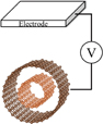
Fig. 1. Structural model of the DWCNT in the FET structure under an applied electric field.
Download figure:
Standard image High-resolution imageFigure 2 shows the distributions of accumulated carriers in the DWCNTs under an external electric field. For both DWCNTs,  @
@ and
and  @
@ , the carrier distribution indicates that the carrier accumulation is insensitive to the CNT diameter. In contrast, the carrier distribution is sensitive to the carrier species. For hole doping, the injected holes are distributed primarily on the outside of the outer CNT, whereas holes and electrons are absent on the inner CNT. For electron doping, the electrons were distributed on the electrode side of the outer CNT and extended throughout the outer wall of the inner CNT. As a result of the accumulated electron distribution, holes were induced inside the outer and inner CNTs, forming a coaxial cylindrical capacitor of nanometer diameter. In addition to the carrier species, the carrier concentration also induces further variation in the carrier distribution: For the
  @
@ DWCNTs with 0.1e doping, no accumulated electrons were present on the inner CNT. Hence, the distribution of the accumulated carriers depends on the carrier species and concentration.
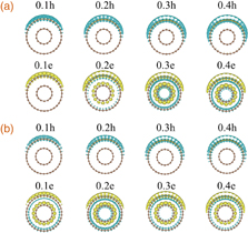
Fig. 2. Isosurfaces of the accumulated carriers in (a)  @
@ and (b)
  @
@ nanotubes. In each panel, 0.1–0.4h and 0.1–0.4e denote the injection of 0.1–0.4 holes and 0.1–0.4 electrons, respectively. Yellow and blue isosurfaces indicate regions where the number of electrons and holes, respectively, increases under the electric field.
Download figure:
Standard image High-resolution imageFigure 3 shows contour plots of the electrostatic potential and vector plots of the electric field of the DWCNTs under an external electric field. For hole doping, because there are no accumulated carriers inside the outer CNT, the electrostatic potential is flat inside the outer CNT, corresponding to an absence of the electric field inside the DWCNT. This fact indicates that the holes injected into the outer CNT strongly screen the external electric field. In contrast, for electron doping, a radial electric field is induced between the inner and outer CNTs for both DWCNTs, because accumulated electrons and holes are distributed coaxially outside the inner CNT and inside the outer CNT, respectively. For the  @
@ DWCNTs under low electron concentrations, no radial electric field between the inner and outer CNTs is present because of the absence of an accumulated electron distribution on the inner CNT. Therefore, coaxial distributions of electrons and holes between the inner and outer CNTs cause the unusual electric field inside the DWCNT under high electron concentrations.
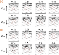
Fig. 3. Contour plots of the electrostatic potential and vector plots of the electric field of (a)  @
@ and (b)
  @
@ DWCNTs. In each panel, 0.1–0.4h and 0.1–0.4e denote the injection of 0.1–0.4 holes and 0.1–0.4 electrons, respectively. Red circles in each panel denote the atomic position.
Download figure:
Standard image High-resolution imageThe electronic band structures and the square of the wave function at the top of the valence (HO) band and the bottom of the conduction (LU) band give theoretical insight into the physical mechanism of the peculiar distribution of the accumulated carriers and electric field (Fig. 4). The electronic energy band and wave functions for the LU and HO bands are qualitatively the same for the  @
@ and
and  @
@ DWCNTs. The DWCNTs have a staggered (type II) band-gap structure. The HO and LU states are distributed over the outer and inner CNTs, respectively, so the band gap is smaller than that of each CNT. According to the distribution of the HO states, the injected holes are accommodated in the HO states localized on the outer wall of the DWCNT, exhibiting the extended profile of a π state. In contrast, for electron doping, the electrons are accommodated in an LU state associated with the π* state of the inner CNT, leading to an electron distribution that extends throughout the inner CNT. Note that the electron distribution on the upper region of the outer CNT is associated with electrostatic induction by the planar counter electrode.
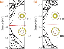
Fig. 4. Electronic energy bands of (a)  @
@ and (b)
  @
@ DWCNTs and wave function at the Γ point of the DWCNTs. The Fermi level is denoted by a horizontal dotted line. HO and LU denote the highest occupied bulk DWCNT state and the lowest unoccupied bulk DWCNT state, respectively.
Download figure:
Standard image High-resolution imageFigure 5 shows the total capacitance of the DWCNTs as a function of the gate voltage for electron and hole doping. The capacitance is almost constant for all gate voltages. The calculated capacitance of the  @
@ DWCNT is 0.1 zF/Å larger than that of the
  @
@ DWCNT for all the gate voltages studied here. The large capacitance of the
  @
@ DWCNT is ascribed to the large-diameter outer CNT. Note that the total capacitance of a DWCNT is 40% smaller than the geometrical (classical) capacitance because of the small density of states in the energy region. For a classical capacitance, the calculated ratio of the capacitance of a
  CNT to that of a
  CNT is 1.04, whereas the ratio of the total capacitance of
  @
@ DWCNTs to that of
  @
@ DWCNTs is 1.03. This discrepancy is ascribed to the effect of the carrier distribution on the inner CNT.

Fig. 5. Capacitance of DWCNTs as a function of the gate voltage for electron or hole injection. Circles and squares denote the capacitance of the  @
@ and
and  @
@ DWCNTs, respectively.
Download figure:
Standard image High-resolution image
The electronic structure of  @
@ and
and  @
@ DWCNTs in an external electric field were studied using density functional theory combined with an effective medium screening model. The calculations showed that carrier accumulation in the DWCNTs depends on the carrier species and concentration. Injected holes were distributed and localized on the electrode side of the outer CNT. In contrast, for electron doping, the electrons were distributed outside the upper part of the outer CNT and extended over the outside of the inner CNT wall, whereas a hole was simultaneously induced inside the outer and inner CNTs and was extended over their entire surfaces. The extended nature of the carriers injected into DWCNTs by a negative gate voltage leads to a radial electric field like that of a coaxial cylindrical capacitor with nanometer diameter. In contrast, because there is no electric field inside the outer CNT, the injected holes screen the external electric field well. We also calculated the capacitance of the DWCNTs with a planar counter electrode. The capacitance of the
  @
@ DWCNT is higher than that of the
  @
@ DWCNT because the outer CNT has a larger diameter in the former case. Furthermore, the total capacitance of the DWCNTs is 40% smaller than the geometrical (classical) capacitance because of the small density of states in the energy region. The present results give a guiding principle for controlling the electronic properties of a DWCNT in a FET structure in terms of the external electric field.
Acknowledgments
This work was supported by JST-CREST Grant Number JPMJCR1532 from the Japan Science and Technology Agency, JSPS KAKENHI Grant Numbers JP17H01069, JP16H00898, and JP16H06331 from the Japan Society for the Promotion of Science, and the Joint Research Program on Zero-Emission Energy Research, Institute of Advanced Energy, Kyoto University. Some of the calculations were performed on an NEC SX-Ace at the Cybermedia Center at Osaka University and on an SGI ICE XA/UV at the Institute of Solid State Physics, The University of Tokyo.