
Abstract
We report the preparation and manipulation of slidable atomic layers in clean, incommensurate van der Waals (vdW) heterostructures. Monolayer and multilayer WS2 grains are grown on graphite and hexagonal boron nitride (hBN) via chemical vapor deposition, and these grains can slide smoothly on graphite and hBN surfaces by manipulation with a tip. Furthermore, this sliding process allows the suspension, tearing, stacking, and connection of the atomic layers. These results demonstrate a novel approach for developing a wide variety of atomic-layer heterostructures with tunable interlayer coupling and an ideal system for studying the superlubricity of incommensurate, highly clean vdW contacts.
Export citation and abstract BibTeX RIS

Content from this work may be used under the terms of the Creative Commons Attribution 4.0 license. Any further distribution of this work must maintain attribution to the author(s) and the title of the work, journal citation and DOI.
The development of novel fabrication and manipulation techniques for van der Waals (vdW) heterostructures based on atomic layers such as graphene, hexagonal boron nitride (hBN), and transition-metal dichalcogenides (TMDCs) is one of the most important challenges for controlling the electrical and optical properties of these materials.1–5) The preparation of vdW heterostructures has mainly been conducted by using two types of methods: transfer3–6) and direct growth.7–13) As-prepared heterostructures are typically immobilized and used without any structural modification. In contrast, an atomically clean contact has ultralow friction, which is called superlubricity.14–16) The superlubricity of layered materials has been a central topic because of interest in the origin of friction as well as potential applications such as frictionless coatings. As a similar model, the interlayer frictional force of similar incommensurate vdW contacts has been investigated for multiwall carbon nanotubes.17–19) The frictional properties of graphene nanoribbons on a gold surface were recently investigated to determine the origin of the superlubricity.20) If we can use this superlubricity for the structural modification of atomic-layer heterostructures, various applications can be realized.
As a first step, it is highly desired to prepare atomic-layer heterostructures with a clean vdW contact. In this work, WS2 grains as slidable atomic layers were grown on exfoliated graphite and hBN via chemical vapor deposition (CVD), as previously reported [Fig. 1(a)].12,13) Graphite and hBN flakes were used as substrates with dangling-bond-free, atomically flat vdW surfaces. Because of their incommensurate stacking and clean interface, it was expected that the TMDC grains grown on these substrates had a small lateral frictional force owing to the small energetic barrier to interlayer sliding and thus could be moved by pushing and pulling. Indeed, this sliding process allowed the suspension, tearing, stacking, and connection of TMDC atomic layers. Our finding provides a novel method for developing vdW heterostructures with tunable interlayer coupling and an ideal system for studying the superlubricity in incommensurate vdW contacts.
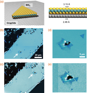
Fig. 1. (a) Schematic of monolayer WS2 grown on graphite. (b, c) Optical images of WS2 grains grown on graphite before and after manipulation. Sliding crystals are indicated by arrows. (d, e) Enlarged images of WS2 grains before and after manipulation. Contrast slightly changes within individual images because several images were connected to cover a wide area of the samples.
Download figure:
Standard image High-resolution imageWS2 was grown on Kish graphite (Type C, Covalent Materials) or hBN flakes using CVD, as previously reported.13) Single-crystal hBN was prepared via a high-temperature and high-pressure method.21) First, graphite and hBN crystals were mechanically exfoliated onto quartz substrates using Nitto tape (SPV-224). For CVD growth, the substrate was placed in a quartz tube (3 cm diameter, 100 cm long) with WO3 powder (Aldrich, 99% purity, 30–80 mg) and sulfur flakes (Aldrich, 99.99% purity, 2 g). The quartz tube was then filled with Ar gas at a flow rate of 100 cm3/min. The temperature of the substrate and the WO3 powder was gradually increased to the sulfurization temperature (1100 °C) over 60 min using an electrical furnace. When the substrate temperature was at the set point, the sulfur was heated at 200 °C for 30 min to supply sulfur vapor to the substrate using another electrical furnace. After the sulfurization, the quartz tube was immediately cooled using an electric fan.
The sliding of the atomic layers was performed using a hand-operated micro manipulator with an optical microscope under atmospheric conditions and a nano-prober system (Hitachi N-6000SS) under vacuum at room temperature. For the nano-prober system, the sliding process was monitored using scanning electron microscopy (SEM). Optical images were recorded using an optical microscope (Nikon Eclipse-LV100D). Photoluminescence (PL) measurements were performed using a micro-Raman spectroscope (Renishaw inVia) with a 532-nm excitation laser.
The multilayer WS2 grains were moved as far as 100 µm on the graphite using a hand-operated micro manipulator, as shown in Figs. 1(b) and 1(c). Despite such a long travel distance, the grains did not undergo a shape change during the manipulation [Figs. 1(d) and 1(e)], which indicates a very small interlayer frictional force between the graphite and the WS2 grains. As shown in the enlarged images, two grains moved close to each other because the larger crystal pushed the smaller crystal.
This result motivated us to fabricate a lateral contact of two atomic layers via controlled sliding, as illustrated in Fig. 2(a). For this purpose, a nano-prober system with piezo-driven manipulators was used to slide atomic layers precisely under SEM observation. This system was used to successfully slide a WS2 grain on the graphite and connect it to another WS2 grain [Figs. 2(b) and 2(c) and Movie S1 in the online supplementary data at http://stacks.iop.org/APEX/10/045201/mmedia]. The lateral contact was stable and was maintained after the tip was removed from the grain.
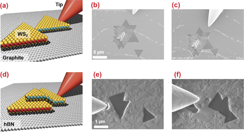
Fig. 2. (a) Schematic and (b, c) SEM images taken before and after the contact of two WS2 crystals grown on graphite. (d) Schematic and (e, f) SEM images taken before and after the stacking of two WS2 crystals grown on hBN.
Download figure:
Standard image High-resolution imageThe type of substrates was determined to be an important factor affecting the nature of the contact between two WS2 grains in the nano-prober system. For example, a WS2 grain grown on hBN was moved on top of another WS2 grain, as shown in Figs. 2(d)–2(f). Interestingly, WS2 grains grown on hBN were frequently inserted into the interlayer between another WS2 grain and the hBN (Fig. S1 in the online supplementary data at http://stacks.iop.org/APEX/10/045201/mmedia). These behaviors have never been observed for grains on graphite substrates, probably because of the charge-up effect of hBN substrates. hBN is an insulator with a bandgap of approximately 6 eV;22) therefore, the WS2 grains and the hBN surface were immediately charged through electron-beam irradiation during the SEM observations, which could have led to the modulation of the interlayer interaction between the WS2 and hBN (or WS2), and/or the aggregation of surface impurities that disturbed the inter-edge contacts. This suggests the possibility of charge- (or impurity-) assisted control for the fabrication of lateral contacts and stacking structures via sliding processes.
This sliding process can be applied to the tearing of monolayer WS2 and to the control of the strain-induced local bandgap modulation. As shown in Figs. 3(a)–3(c), a triangular monolayer WS2 grain was dragged to the lower side. In this case, a part of the crystal was torn during re-dragging to the upper side and separated from the parent crystal [Fig. 3(c)]. These torn grains are clearly observed in the PL intensity map [Fig. 3(d)]. Despite the uniform PL intensity, the parent grain had a large variation of the peak wavelength within a single domain, as evident in the wavelength map of the PL peaks [Fig. 3(e)]. In particular, the low-energy shift and broadening of the PL peaks were observed at one point [Fig. 3(f)]. These changes are interpreted as bandgap narrowing induced by local lattice expansion, which occurred during the sliding process. There was almost no shift in the Raman modes measured at the same locations via PL measurement (Fig. S2 in the online supplementary data at http://stacks.iop.org/APEX/10/045201/mmedia). Raman signals are usually averaged data within the area of the laser spot, whereas PL only provides information about the minimum gap in the measured area depending on the diffusion length of the excitons, as reported in a previous study on strained monolayer MoS2.23) Thus, the sliding process can be used to introduce local lattice strain that leads to the site-selective bandgap modulation of the atomic layers.

Fig. 3. (a–c) SEM images obtained during the manipulation of monolayer WS2 on graphite. Arrows indicate the direction of the tip manipulation. From (a) to (c), the figures are presented in the order of manipulation. Inset in (c) shows a schematic of the WS2 grain tearing. (d) Intensity and (e) peak wavelength maps of the PL of monolayer WS2 grains after the tearing. (f) PL spectra measured at three different points indicated by the symbols in (d). SEM images of WS2 grains on graphite (g) before and (h) after suspension. Inset in (h) shows a schematic of a suspended WS2 grain. (i) PL spectra of bilayer WS2 supported on graphite and suspended in air. X and I indicate the emissions derived from the direct and indirect gaps of bilayer WS2, respectively.
Download figure:
Standard image High-resolution image
The fabrication of a suspended structure of TMDC grains was also demonstrated. When WS2 grains were located near the edge of a substrate, the grains were easily pushed away from the edge, yielding a suspended structure, as shown in Figs. 3(g) and 3(h). The suspended monolayer and bilayer WS2 grains had a far brighter PL than those on graphite substrates [Fig. 3(i) and Fig. S3 in the online supplementary data at http://stacks.iop.org/APEX/10/045201/mmedia]. The PL enhancement was caused by the elimination of the non-radiative process of excitation energy to the graphite substrate. The peak shapes became broad and asymmetric, which is more drastic than substrate-dependent spectral changes.13) This suggests that the suspended structure induced a large inhomogeneous lattice strain in the WS2 atomic layers.
As presented herein, the sliding process can be applied to the fabrication and manipulation of various heterostructures based on atomic layers and strain engineering. Only WS2 grains can move on graphite and hBN surfaces; the interlayer sliding of multilayer WS2 grains has not yet been observed using the present nano-prober system. This indicates that the lateral frictional force between WS2 and graphite (hBN) is far smaller than that between different WS2 layers. These differences can be understood from the perspective of commensurate and incommensurate stacking in the present vdW heterostructures. For WS2/graphite (hBN) stacking, a large lattice mismatch leads to incommensurate stacking (in-plane lattice constants are 3.15 Å for bulk WS2,24) 2.46 Å for graphite,25) and 2.50 for bulk hBN26)), as shown in Fig. 1(a), which reduces the lateral frictional force at the interface. In contrast, the commensurate stacking of WS2 layers generates stable geometries, such as 2H and 3R polytypes. Breaking such stable geometries requires a large energetic barrier to interlayer sliding compared with that for incommensurate stacking. The cleanness at the interface of directly grown WS2 grains and exfoliated graphite and hBN flakes contributes to the low lateral frictional force. Thus, the determination and control of the frictional force in future research is expected to contribute to the study of nanoscale tribology and lead to the development of microelectromechanical systems based on vdW heterostructures with ultralow friction.
Acknowledgments
The authors acknowledge H. Akinaga and K. Hayama (AIST) for performing the manipulation experiments. A part of this work was conducted at the AIST Nano-Processing Facility, which is supported by the "Nanotechnology Platform Program" of the Ministry of Education, Culture, Sports, Science and Technology, Japan. This work was supported by JSPS KAKENHI Grant Numbers JP15H05412 and JP16H00918.