
Abstract
An Nd3+:YAG pulsed laser was employed as a light source for two-photon photoemission from organic semiconducting thin films in low vacuum and air. Photoionization by the two-photon process was confirmed in both the environments by measuring photoemission current. By constructing a pump–probe system, photoemissions from transient species formed by the pump light irradiation were detected by probe light irradiation as a result of a linear increase in the photocurrent with the pump power via a one-photon process. Thus, we propose a novel method called two-photon photoelectron yield spectroscopy to determine the excited-state energy levels in ambient environments.
Export citation and abstract BibTeX RIS

Content from this work may be used under the terms of the Creative Commons Attribution 4.0 license. Any further distribution of this work must maintain attribution to the author(s) and the title of the work, journal citation and DOI.
This article was made Open Access on 27 February 2017
Understanding the electronic structure of organic semiconducting thin films is crucial for various organic electronics, such as organic light-emitting diodes (OLEDs), organic thin film transistors, and organic photovoltaics (OPVs).1–3) Thus far, a number of studies have been conducted on the highest occupied molecular orbital (HOMO) band by using ultraviolet photoelectron spectroscopy (UPS). The energy position and structure of the HOMO band determines hole injection/extraction barrier at interfaces in organic devices and the inherent hole transport properties of organic materials, respectively.4–7) The same aspects can be studied for the lowest unoccupied MO (LUMO) as well by using inverse photoelectron spectroscopy (IPES). Recent progress in IPES achieved by employing a low-energy electron source has overcome a long-term issue in the IPES technique, i.e., radiation damage in organic thin films by high-energy electron-beam irradiations; this progress has provided a possibility to investigate the nature of electrons in organic semiconductors.8–10)
Both UPS and IPES extract information on the ground-state energy levels of materials. On the other hand, the excited-state energy levels of organic materials, which are essential for the performance of OLEDs or OPVs,11,12) can be studied by combining a pump–probe technique using an ultra-short pulsed laser as the light source with UPS. This combination is called time-resolved two-photon photoelectron spectroscopy (TR-2PPE).12–16) In this method, following the HOMO–LUMO transition induced by pump laser pulses, an excited state of organic molecules in thin films is formed. Before deactivating the excited state, the second (probe) laser pulse is irradiated as a function of delay time (Δt) between the pump and probe laser pulses to eject electrons from the LUMO level in the excited singlet (S1) or triplet (T1) states. Similar to UPS, the kinetic energy of ejected electrons is measured using an electron analyzer, and as a result, the binding energy of the LUMO level can be determined. By acquiring results for different values of Δt, the lifetime (τ) of the S1 and T1 states can also be evaluated.12,16) However, in general, the construction and operation of the TR-2PPE apparatus involves very high cost, and the technician conducting the measurement requires skills for both photoelectron and laser spectroscopies. As in UPS and IPES, the measurement environment is restricted to ultrahigh vacuum (UHV) conditions, limiting the in situ study of the effect of the environment on excited-state energy levels.17)
Photoelectron yield spectroscopy (PYS) is a method that can be used to determine the ionization potential (IP) or the work function of materials of interest.17–20) Here, we rephrase the term IP to IPS0, which is the IP in the ground state (S0), to distinguish it from the IP determined in excited states, which will be described later. In contrast to UPS, PYS does not analyze the kinetic energy of photoelectrons; it measures the energy of the irradiated stationary light upon photoemission [Figs. 1(a) and 1(b)]. The photoelectrons are collected typically to ring or mesh electrodes, which are placed close to the sample surface, by applying a collection voltage between the electrodes and sample surfaces, which enable the determination of IPS0 in various environments, including low vacuum and even air. However, since the photoemission of PYS is a one-photon process, conventional PYS cannot access the LUMO levels.20)

Fig. 1. Schematic explanation of (a) PYS and (c) 2P-PYS methods. For PYS, the energy of irradiated stationary light ( ) is varied and IPS0 is evaluated from the cut-off energy for photoemission (b). For 2P-PYS, the ionization process is performed by following two processes. (c1) Formation of an excited state by HOMO–LUMO transition due to the irradiation of the pump laser pulse. (c2) Photoemission from the LUMO level in the S1 or T1 state due to the irradiation of the probe laser pulse. Analogous to PYS, the cut-off energy of the probe light for the photoemission from the S1 or T1 state will be IPS1 or IPT1, respectively.
Download figure:
Standard image High-resolution imageIn this paper, we propose a novel method to study excited-state energy levels that overcome the above-mentioned difficulties of TR-2PPE by combining PYS and TR-2PPE into a method called two-photon photoelectron yield spectroscopy (2P-PYS). For 2P-PYS, we use an ultra-short pulsed laser instead of the stationary light source used in PYS. As in TR-2PPE, the pump laser pulse is firstly irradiated on samples to induce the HOMO–LUMO transition [Fig. 1(c1)]. Subsequently, the probe laser pulse is irradiated to eject electrons from the LUMO level. During this time, the energy of the probe light is varied from a value below the IPS0 of the samples. Analogous to PYS, the light energy needed for the photoelectric effect from the LUMO level corresponds to the IP of the LUMO level in the excited state, which is the IP of either the S1 (IPS1) or T1 (IPT1) state, depending on Δt [Figs. 1(c2) and 1(b)]. Notably, IPS1 and IPT1 are different from the electron affinity (EA) [Fig. 1(a)] obtained by IPES. EA is defined as the energy required to add one electron to the LUMO level in the S0 state. The advantages of 2P-PYS are that (1) the measurement environment is not limited to the UHV condition, as in PYS; (2) the measurement system does not require an electron analyzer and a UHV system, resulting in lower development costs and easier handling of 2P-PYS compared to TR-2PPE; (3) the time-resolve measurement provides information on the excited-state dynamics of the S1 or T1 state, similar to TR-2PPE. Here, we constructed a prototype 2P-PYS system and addressed two fundamental issues for 2P-PYS by using thin films of a typical organic semiconductor, pentacene (PEN, C22H14): (1) whether photoemissions by a two-photon process can be measured in technically soft environments, such a low vacuum and even air, with reasonable sensitivity, and (2) if the issue (1) is valid, whether photoemission from transient species can be distinguished from the simultaneous events of photoemission from the ground-state energy levels by using a pump–probe technique.
PEN (purity: 99.995%) purchased from Aldrich was used without further purification. For the substrates, Si(100) wafers covered with native-oxide and glass substrates coated with indium tin oxide (ITO substrates; Geomatec FLAT ITO) were utilized as received. PEN thin films were fabricated on the substrates kept at 295 K by thermal sublimation (base pressure ∼10−7 Pa). Nominal film thicknesses (15 or 21 nm) and deposition rates (0.1–0.2 nm/min) were measured with a water-cooled quartz microbalance. PEN thin films on Si wafers were characterized by UPS at the beamline 2B in UVSOR (Okazaki, Japan), where a hemispherical electron analyzer, R3000 (Scienta Omicron), is installed. For UPS, the energy of the light source, energy resolution of the apparatus, and angles of incident light and emitted electrons were set as 28 ± 0.1 eV, 30 meV, 45°, and 0° (normal emission), respectively.
The test apparatus of 2P-PYS was constructed in-house based on the third harmonic (TH) of fundamental light (1064 nm) of a Nd3+:YAG laser [355 nm wavelength, ∼150 ps full width at half maximum (FWHM) pulse, 10 Hz repetition, and 0.28 cm2 spot size]. A schematic of the set-up is shown in Fig. 2. The TH light (355 nm), which was utilized through a harmonic beam splitter, was separated as pump and probe light beams by using a half mirror. Both the pump and probe lights were introduced to the sample through a lithium-fluoride window and the center of a copper ring collector. The samples and ring collector were kept in a stainless steel (SUS) vacuum chamber (Fig. 2), to reduce electromagnetic noise. During the measurements, a collection voltage of −200 V was applied between the collector and sample with a space of ∼1 mm, and a compensating current flowing from the earth to the sample due to the photoemission was measured using a Keithley 6430 sub-femtoamp remote source meter with an accumulation time of 1 s. In the present laser irradiation conditions, no clear sample degradation was observed. For pump–probe measurements, Δt was varied using a delay stage.

Fig. 2. Schematic of the experimental set-up, photograph of the measurement chamber, and chemical structure of PEN.
Download figure:
Standard image High-resolution imageBy measuring UPS, the IPS0 of the PEN (21 nm)/Si system was determined to be 4.99 eV (Fig. S1 in the online supplementary data at http://stacks.iop.org/APEX/10/022401/mmedia). This value is much higher than the photon energy of the TH light of Nd3+:YAG laser (3.49 eV), the laser energy corresponds to the S0 → S3 transition of PEN thin films.21) Thereby, the photoemission from the PEN thin film is not expected by the one-photon process, but it is possible through the two-photon process as the light energy of two photons i.e., 6.98 eV, exceeds IPS0. Figure 3 shows the laser-power dependence of photoionization current of the PEN (21 nm)/Si system measured under a low vacuum of 0.1 Pa. Here, we used only a probe laser pulse and took the averaged current at different laser powers, which included a dark current of 5 ± 2 fA. Figure 3 indicates that the photoionization current shows a quadratic increase with respect to the laser power. This clearly demonstrates that the photoionization of the PEN thin film can occur through the two-photon process. A maximum current of 270 pA was obtained at a laser power of 36.5 mW/cm2.
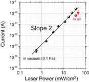
Fig. 3. Laser power dependence of the photoionization current of the PEN (21 nm)/Si system. The solid line represents quadratic dependence. The measurements were conducted from a low laser power in vacuum (0.1 Pa).
Download figure:
Standard image High-resolution imageThe effect of the measurement environment was also investigated. After the final measurement in vacuum (Fig. 3), the sample was exposed continuously to air and the photocurrent was measured under the same laser power condition. The current was decreased by a factor of 4 (red circle in Fig. 3), compared to that measured in low vacuum. However, the observed current of 65 pA in air is still much larger than the detection limit of our set-up of ∼2 fA. This presents a possibility of studying the effect of the atmosphere on the excited states by using the photoemission technique since such an effect has been studied only for ground-state energy levels using high-resolution UPS,22) and the effect on excited-state energy levels remains unclear.
After demonstrating photoionization by single laser pulses for the PEN/Si system in ambient air and vacuum, we next conducted pump–probe measurements in low vacuum (0.1 Pa). A sample of PEN thin films (film thickness ∼15 nm) was newly prepared on ITO substrates, which is a practically relevant substrate for OLEDs and OPVs. Before the measurements, we confirmed that the photoemission from the conducting ITO substrates is negligibly less than that obtained from the PEN thin films by comparing the laser power dependence. The value of Δt was varied using a delay stage from −254 to 3007 ps. For the measurement of Δt dependence, we note here that all the events related to the excited-state dynamics of PEN thin films, i.e., the formation and deactivation of the S1 state and formation of the T1 state via an inter-system crossing, are considered to occur in the time scale of one pulse of our laser, ∼150 ps, and the long-lived T1 state, which has τ > 100 ns, would remain beyond the Δt of the pulse width [see the dynamics of PEN thin films in Fig. 4(b)].12,23) First, we present the results of independent and simultaneous irradiation of pump and probe laser pulses. Figure 4(a) shows the time-sequence current data of the PEN/ITO system obtained with pump and probe light irradiation at Δt ∼ 0 s. The experiment was conducted with the following steps: no light condition → only pump light irradiation → only probe light irradiation → simultaneous irradiation of pump and probe light → no light condition. The average current at each process is tentatively defined as Idark, Ipump, Iprobe, and Ipump&probe, and their values were observed to be 12, 226, 69, and 465 fA, respectively. Ipump&probe does not match the sum of Ipump and Iprobe; even considering the offset of Idark for each current, the excess current of Ipump&probe (ΔI) = [(Ipump&probe − Idark) − (Ipump + Iprobe − 2Idark)] is 182 fA. As observed for the PEN/Si system in Fig. 3, photoionization by the simultaneous two-photon process of PEN thin films occurs with a quadratic relationship to the power of the irradiated light source. Therefore, if two independent pulses are temporally and spatially overlapped, photoionization will occur more efficiently compared to that through the independent irradiation of two pulses, resulting in the appearance of ΔI as shown in Fig. 4(a).
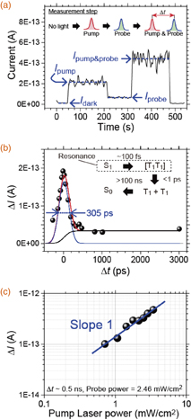
Fig. 4. (a) Test example of pump–probe light irradiation for the photoionization of PEN/ITO systems at Δt ∼0 s in low vacuum (0.1 Pa). The measurement sequence with various irradiation conditions is shown in the inset. The values of Idark, Ipump, Iprobe, and Ipump&probe are indicated by broken lines. Laser power of the pump and probe light source are 1.25 and 0.79 mW/cm2, respectively. (b) ΔI depending on Δt. Black and blue lines are the fitting results obtained using a Gauss function and step function, respectively. The red line is the sum of two fitting results. The laser power of pump and probe light sources is the same as in (a). The inset flow chart indicates the excited-state dynamics of PEN thin films reported in Refs. 12 and 23. [T1T1] and T1 + T1 indicate a multiple triplet exciton and two excitons separated by single fission, respectively. (c) Pump laser power dependence of ΔI obtained with a fixed probe power of 2.46 mW/cm2.
Download figure:
Standard image High-resolution imageNext, we measured ΔI as a function of Δt by fixing the laser power of pump and probe light, respectively. In Fig. 4(b), the obtained ΔI values are distributed as a Gauss function around Δt = 0 s, with a maximum of ∼192 fA, and the ΔI remains almost constant at ∼30 fA above Δt ∼ 400 ps. We simulated the ΔI behavior by using a Gauss function (for the first part) and step function (for the later plateau part). From a least-square fit [see Fig. 4(b)], we obtained an FWHM of 305 ps for both the functions, which is close to the value expected from the electric-field distribution produced by the temporally overlapped pump and probe pulses, ∼212 ps ( ). This implies that the first Gauss distribution is mainly attributed to the two-photon process from the ground state under the condition of temporal overlap of two pulses, and the later component originates from a transient species formed by the photoabsorption of the PEN thin films. In this context, the slightly larger FWHM of 305 ps may be caused by missing a step function to cover the ΔI at Δt < 0 ps regime, which originates from a pump light induced-photoionization of transient species produced by the former coming probe light pulse.
To guarantee photoemission from the transient species, we investigated the laser-power dependence of ΔI at the pump–probe condition in which only the pump light power was varied to change the concentration of transient species formed initially in PEN thin films. The value of Δt was set to 0.5 ns, at which two pulses are not temporally overlapped. Figure 4(c) shows that ΔI increases linearly with the laser power of the pump light. This demonstrates that the photoemission occurred through a one-photon process. This constitutes evidence for photoemission from the transient species by the pump–probe technique because, as mentioned above, the photoemission from ground-state energy levels requires simultaneous two-photon absorption; the linear increase of ΔI is caused by the linear increase of the concentration of the transient species via the one-photon process of the pump light irradiation. Consequently, the binding energy of the transient species is determined to be less than the energy of the TH light of 3.49 eV.
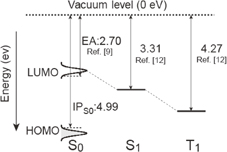
All the results presented here indicate that the photoionization by laser pulse irradiation can be detected in organic semiconducting thin films both in vacuum and air, and more importantly, transient species in the films can be investigated using a pump–probe technique. These investigations are indispensable to validate 2P-PYS. As mentioned in the introduction, the next and final step is the measurement of the threshold energy of photoionization from S1 and T1 states for determining IPS1 and IPT1, respectively. We emphasize that this step is also important for elucidating the fundamental mechanism underlying the photo-physical properties of organic semiconducting thin films. In this paper, we used the TH light of a Nd3+:YAG laser (3.49 eV) as a light source, and its energy is significantly greater than the EA of PEN/ITO systems, 2.70 eV, as determined by using IPES (Fig. 5).9) However, this value may not be appreciable for the present case because organic semiconducting thin films usually show a large exciton binding energy ranging from several hundred meV to values greater than 1 eV.24,25) Therefore, the EA values for IPS1 and IPT1 will be different. For instance, the peak energies of the LUMO level in the S1 and T1 states of PEN thin films grown on a C60/Au(111) system in TR-2PPE spectra have been reported to be 3.31 and 4.27 eV, respectively.12) According to the results of TR-2PPE, photoionization by the one-photon process is possible for S1 but not for T1. Even though the energy of the T1 level will be broadened to some extent, as experimentally observed for the LUMO band in Ref. 12, because of intermolecular interaction and inhomogeneity of the film structures, the energy difference of 0.78 eV between the TH light and T1 level may be too large for photoionization by the one-photon process. In this context, one question remains regarding the origin of the transient species we observed. To understand and reveal the origin of the transient states, it is again highly important to complete the development of 2P-PYS and compare the spectra of 2P-PYS and TR-2PPE, both of which are currently being developed by us.
Fig. 5. Electronic structure of PEN thin films. The EA obtained using IPES and the LUMO level in the S1 and T1 states are taken from Refs. 9 and 12, respectively.
Download figure:
Standard image High-resolution image
Acknowledgments
We would like to thank UVSOR staff members for their technical support and Professor H. Ishii and Dr. H. Kinjo (Chiba University) for their discussion on the construction of the measurement system. This research has been supported by JSPS KAKENHI Grant Number 16K17975.