

Abstract
This study aims to investigate the creep motion of a magnetic domain wall (DW) induced by spin-Hall torque (SHT) in a Ta/Co–Ni/Pt hetero-structured thin wire using photoemission electron microscopy. The displacement of the DW was recorded every time after the duration of an electric current pulse. Results revealed that the existence of pinning centers and the inhomogeneity of the thermal diffusion property of the wire may result in an unstable DW motion. On the contrary, this data also suggested that the SHT induced from both the Ta and Pt layers can significantly improve the DW velocity, which was found to be three orders of magnitude larger than that previously reported for the MgO/Co–Ni/Pt system (Taniguchi et al., Appl. Phys. Exp. 7, 053005 (2014)).
Export citation and abstract BibTeX RIS
1. Introduction
Since the first manifestation of the electric-current controllability of magnetic domain walls (DWs) in thin-wired magnetic films,1) several extensive studies have been conducted2–4) to realize the non-volatile magnetic memories such as racetrack memories.5) Adiabatic spin transfer torque (STT) is the main driving force that causes the DW motion; however, it was recently demonstrated that the spin-Hall torque (SHT) can also be utilized to move DWs,6,7) given that a chiral Néel wall is formed due to the Dzyaloshinski–Moriya interaction (DMI)8) caused by inversion-symmetry-breaking, e.g. heterostructures which comprise perpendicular magnets and heavy metals are formed in the wire. For both the STT and SHT, even a low current density, which is well below the DW depinning threshold, can exert DW displacement in the form of creep motion by thermal activation,9–14) thus drawing attention to the development of energy-efficient DW memories. Nevertheless, the unstable nature of creep motion, i.e. the variation of DW mobility due to pinning site interferences, hampers the construction of reliable devices. Under these circumstances, it is essential to clarify the factors causing the stochastic or uncertain behavior in DW creeping.
Herein, we investigated DW creep motion by SHT in a perpendicularly magnetized Co–Ni thin-wired film by photoemission electron microscopy and X-ray magnetic circular dichroism effect (XMCD-PEEM). Systematic pulse-by-pulse observations of DWs under different current densities and current pulse durations revealed the influence of the inhomogeneity of the wire's thermal diffusion property and pinning defects on the DW motion. These observations also suggested that sandwiching the Co–Ni layer between two heavy metal layers with opposite spin-Hall angles dramatically improved the DW velocity.
2. Experiment
A Co–Ni thin film was grown using magnetron sputtering with a designed multilayered structure Ta (4 nm)/Co(0.3 nm)/Ni (0.6 nm)/Co (0.3 nm)/Pt (2 nm)/Ta (4 nm)/SiO2–Si substrate. The film was fabricated into a thin-wired shape (width: 1 μm, length: 8 μm) with Au electrodes using electron beam lithography [Fig. 1(a)]. Magnetic domain imaging by XMCD-PEEM at Co L2,3-edge was performed at the BL25SU soft X-ray beamline in SPring-8.15–17) Since XMCD-PEEM is a contactless optical probe with high resolving power, it is known to be a promising method for imaging the domain of magnetically volatile microstructures.18) The sample magnetization was saturated by a Nd–Fe–B permanent magnet prior to the installation of the PEEM measurement chamber. Then, an initial DW was created by applying a local magnetic field via a strong current flow along the Au through line [90 mA, 1 μs pulse, red arrow in Fig. 1(a)]. Domain structures were systematically recorded every time after giving one current pulse in situ along the Co–Ni wire [blue arrow in Fig. 1(b)]. It was confirmed that the waveforms of all the current pulses used in this experiment were perfectly rectangular. All experiments were performed at the room temperature.

Fig. 1. (Color online) (a) Schematic drawing of Co–Ni wire with Au electrodes. (b) Magnetic domain images of Co–Ni wire after applying i pulses (50 ms width) of 1.1 × 10¹¹ A m−2 of electric current.
Download figure:
Standard image High-resolution image3. Results and discussion
Figure 1(b) shows the evolution of the DW in the Co–Ni wire after applying i pulses of 1.1 × 10¹¹ A m−2 for a duration (τpulse) of 50 ms. Hereafter, the current density values are represented by those averaged out in the entire multilayer (Jmultlayer). To convert to current densities flowing in the Pt layer (JPt) and the Ta layer (JTa), multiply the factors of 1.09 and 0.86, respectively. The positions of the domain boundaries were identified with a lateral resolution of ∼300 nm at the full width at half maximum. As reported earlier for SHT-driven DW dynamics, the DW moved along the direction of the current flow, contrary to the STT-driven cases, where DWs traveled along the electron flow direction. The plots in Figs. 2(a)–2(d) show the DW positions (red dots with lines) together with the traveling distances per pulse (blue bars) for four different pulse conditions (Jmultlayer varies from 5.6 × 10¹⁰ to 4.5 × 10¹¹ A m−2 and τpulse varies from 2 s to 50 μs); the plots for Fig. 1(b) correspond to Fig. 2(b). Overall, the amount of DW shift fluctuated considerably, and in particular, tilted domain boundaries were reproductively observed at around 2 μm away from the start point [for 1.1 × 10¹¹ A m−2 and 50 ms case, see Fig. 1(b) (i = 3, 4)]. This result indicates that the pinning sites concentrated at this position interrupt the DW motion. Nevertheless, since the Co–Ni film's relatively large perpendicular magnetic anisotropy prefers to minimize the area of the domain boundary, DW is restored to the original straight domain (without maintaining the tilted shape) once it passes through the prominent pinning center (i > 5).
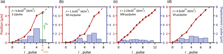
Fig. 2. (Color online) Position (red lines) and displacement per pulse (blue bars) of DWs vs. number of current pulses for (a) 5.6 × 10¹⁰ A m−2, 2 s/pulse (b) 1.1 × 10¹¹ A m−2, 50 ms/pulse (c) 2.23 × 10¹¹ A m−2, 500 μs/pulse and (d) 4.5 × 10¹¹ A m−2, 50 μs/pulse. Green and orange arrows in (a) show examples of dsum and Npulse, respectively, used to extract the average velocity value, vav.
Download figure:
Standard image High-resolution imageReviewing the DW movement, as summarized in Figs. 2(a)–2(d), some common tendencies were found, which are as follows: i) small DW displacement at approximately 0–3 μm from the starting point (region I), ii) relatively large DW displacement per pulse around the middle of the wire (3–6 μm, region II), and iii) slightly reduced shift around the exit (6–8 μm, region III). The dense pinning centers were considered to slow down the DW motion around region I, whereas the smooth DW motions were realized around region II which had no prominent obstacle. As for the slight reduction in the DW displacement around region III, a large Au exit electrode situated close to this region likely to acted as a thermal bath and weakened the thermal activation (note that the velocity of the creep motion increases with an increase in the device temperature13)). Although it is unclear why the movement throughout the whole wire for the case of Fig. 2(c) ( A m−2, τpulse = 500 μs), is exceptionally constant, the application of short-step pulses seems to alleviate the influence of pinning sites (in this case, it took 11 pulses for the DW to reach the exit electrode, in contrast to the 5–7 pulses required in the other cases).
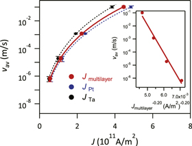
The current density dependence of the average DW velocities, vav, obtained from the series of measurements [Figs. 2(a)–2(d)] is summarized in Fig. 3 (red dots). Here, vav is defined as dsum/(τpulse Npulse), where dsum and Npulse denote the final position before reaching the end of the wire and the number of pulses required to reach dsum, respectively [see arrows in Fig. 2(a)]. A fitting result obtained using a universal Arrhenius scaling relation,19) log10vav ∝ fμ, is overlaid by a red line, where f and μ denote an external force (current density) and a characteristic exponent, respectively. The best fit was obtained by substituting 0.20 for the μ parameter, the value close to 0.25 with which the DW dynamics is categorized into a universality class with random bond. The result is plausible for the motions induced by the SHT in metallic magnets.9–11) Surprisingly, the DW velocity under Jmultlayer = 2.23 × 10¹¹ A m−2 have marked ∼1 × 10⁻³ m s−1, which is significantly higher than the value ∼1 × 10⁻⁶ m s−1 reported by the authors' collaborating group with a similar Co–Ni-based device structure.14) A factor that may have contributed such a dramatic improvement is the difference in the thermal diffusion property. However, the multilayered structure of the thin wire used for the proposed experiment, Ta (4 nm)/Co–Ni(1.2 nm)/Pt (2 nm)/Ta (4 nm)/SiO2Si sub., does not contain heat-blocking layer, which is in contrast to Ta (4 nm)/Pt (2 nm)/MgO(1 nm)/Co–Ni(1.2 nm)/Pt (2 nm)/Ta (4 nm)/SiO2–Si sub. (of Ref. 14), where 1 nm thick layer of insulating MgO was inserted. Despite the difference in the measurement conditions, i.e. the measurement of this study were conducted in vacuum, whereas the measurement of Ref. 14 were conducted in air, the thermal-insulation effect of the solid MgO layer may overweigh that of the gas-free surface. The high DW mobility herein was attributed to enhanced spin-Hall effect, due to the doubly stacked heavy element films, Pt and Ta, directly under and over the Co–Ni layer, respectively. Since the spin-Hall angles of Pt and Ta have opposing signs,20) the spin-Hall effect may significantly improve when these layers are deployed on the different sides of the Co–Ni layer. Although the difference in DMI effect can be another contributing factor to change the DW mobility, net DMI effect may rather be compensated in the Ta/Co–Ni/Pt system (the chiral Néel wall may be less stabilized), since the chirality of the Néel wall is reported to be identical between Pt/Co–Fe/MgO and Ta/Co–Fe/MgO systems.7)
Fig. 3. (Color online) Plot of vav (log10 scale) vs. Jmultilayer (red dots). Error bars show standard deviations of pulse-to-pulse variations in the DW shifts. vav vs. JPt (blue dots) and JTa (black dots) are also shown for reference. Solid and dotted lines show the fitting results with a creep exponent μ = 0.20. Inset shows a log10 (vav) vs. J−0.20multilayer plot of the same data.
Download figure:
Standard image High-resolution image
4. Conclusion
SHT-induced DW creep motion was investigated in a perpendicularly magnetized Co–Ni thin-wired film with asymmetric sandwiching layers. The results demonstrated that local inhomogeneity in the thermal diffusion property as well as the existence of pinning centers were the main causes of unstable or uneven DW creep motion in the thin magnetic wires. It was also found that the magnetic layer sandwiched by two heavy element layers with opposing spin-Hall angles showed dramatic improvement in DW velocity, which may serve to achieve energy-efficient DW creep motions.
Acknowledgments
The experiments at the BL25SU in SPring-8 were performed with the approval of the Japan Synchrotron Radiation Research Institute (JASRI) (Proposal Nos. 2014B1264, 2015A2037). This work was partially supported by Grants-in-Aid for Young Scientists (B, 26790076 and A, 17H04920) from the Japan Society for the Promotion of Science, the Photon and Quantum Basic Research Coordinated Development Program of the Ministry of Education Culture, Sports, Science and Technology, and JASRI's domestic competitive fund (GIGNO project). The authors would like to thank Enago (www.enago.jp) for the English language review.