
Abstract
1550 nm wavelength photonic-crystal surface-emitting lasers (PCSELs) are attractive for optical communication and eye-safe sensing applications. In this study, we present InP-based PCSELs featuring a double-lattice photonic-crystal structure designed for high-power single-mode operation at a wavelength of 1550 nm. These PCSELs demonstrate output powers exceeding 300 mW under continuous-wave conditions at 25 °C. Additionally, highly stable single-mode oscillation with a side-mode suppression ratio of over 60 dB is verified at temperatures from 15 °C to 60 °C. Measurement and simulation of photonic band structures reveal the impacts of the threshold gain margin and optical coupling coefficient on the single-mode stability.
Export citation and abstract BibTeX RIS

Content from this work may be used under the terms of the Creative Commons Attribution 4.0 license. Any further distribution of this work must maintain attribution to the author(s) and the title of the work, journal citation and DOI.
Photonic-crystal (PC) surface emitting lasers (PCSELs) have attracted much attention as light sources for various applications, such as light detection and ranging (LiDAR), material processing, and optical communications including free-space transmission, driven by their capability of single-mode operation, high optical power, and high-quality and narrow-divergence-angle beams. 1–7) These features cannot be simultaneously achieved with conventional semiconductor lasers. The PCSELs utilize a two-dimensional (2D) PC deployed in the vicinity of an active layer as a cavity. Lasing oscillation is achieved in the form of a broad-area 2D standing wave at a singularity point (typically Γ) in the photonic band structure. By properly designing the unit cell of the 2D PC structure, optical couplings originating from 180° and 90° diffractions can be controlled to enable single-mode in-plane oscillation across a large area with sufficient emission in the vertical direction. Recently, a design concept has been proposed featuring double-lattice PC structures, 8,9) which are shown to enable flexible control of such optical couplings. By employing the double-lattice PC structure in GaAs-based PCSELs operating at wavelengths in the range of 900–1000 nm, 8–13) CW single-mode lasing with large emission areas up to a 3 mm diameter has been demonstrated, with an output power of up to 50 W with a narrowly diverging beam. 10) PCSELs operating at various other wavelengths have been also reported using different material systems including GaN-based PCSELs (400–550 nm), 14,15) InP-based PCSELs (1300–1600 nm), 16–20) as well as far-infrared (terahertz) quantum cascade PCSELs. 21) Among these wavelengths, 1550 nm is particularly important for fiber-based optical communications for the purpose of minimizing transmission loss. Additionally, for LiDAR applications, including frequency-modulated continuous-wave (FMCW) systems, the use of a 1550 nm wavelength is mandatory for eye safety, because light of this wavelength is mostly absorbed in the crystalline lens of the eye before reaching the retina. For such applications, stable single-mode CW lasers are in high demand. PCSELs are expected to be able to meet this demand, as they have the potential to achieve higher single-mode output power than conventional distributed feedback (DFB) lasers. 22) Despite their industrial importance, there has been limited progress on the development of 1550 nm wavelength PCSELs. While single-mode lasing at a peak output power of up to 100 mW under pulsed conditions has been reported using 1550 nm wavelength InP-based PCSELs, 17) CW operation of these PCSELs at output powers of hundreds of milliwatts has not been achieved, in contrast to GaAs-based 13) and GaN-based ones. 23)
In this paper, we develop 1550 nm wavelength PCSELs, leveraging our 1300 nm wavelength InP-based PCSEL technologies 19,20,24) that include dry-etching and regrowth processes along with the double-lattice PC structure. The design of the double-lattice PC structure is also improved to realize stable high-power single-mode operation at 1550 nm wavelengths. We achieve single-mode lasing at a wavelength of 1550 nm with a CW output power exceeding 300 mW at 25 °C for a 200 μm diameter device. To our knowledge, this marks the highest CW output power ever reported for PCSELs in the 1550 nm wavelength range. Furthermore, we demonstrate stable single-mode oscillation with a side-mode suppression ratios (SMSRs) exceeding 60 dB over a wide range of injection currents of up to 2 A and operating temperatures of up to 60 °C. Finally, we clarify the origin of the stable single-mode operation based on the photonic band structure of the PCSEL.
Figure 1 illustrates a schematic of our 1550 nm wavelength PCSELs. The fabrication process follows the same procedure described for 1300 nm PCSELs in Ref. 24. Epitaxial layers are grown on a n-InP substrate using metal-organic vapor-phase epitaxy. First, a PC pattern is formed through electron-beam lithography and dry-etching processes. Subsequently, an InP spacer is overgrown to encapsulate the air holes, followed by the growth of an active layer composed of four InGaAsP quantum wells, a p-InP cladding layer, and a p+-GaInAs contact layer. The air-hole shapes after the regrowth process are shown in references. 19,20) Deep air holes with heights of over 500 nm are obtained in spite of their small size. Note that the advantage of this fabrication process is that, by growing the active layer atop the PC layer after the dry-etching step, the risk of damaging the active layer through dry etching of the deep air holes is avoided, enabling the PC structure to be closer to the active layer. The diameter of the p-electrode (L), which determines the device size, is set to L = 200 μm. The n-electrode features a circular window through which the light is emitted, while the p-electrode serves as a backside reflector to enhance the slope efficiency. The composition and alloy conditions of the electrodes have been precisely tuned to provide a relatively high p-electrode reflectivity of approximately 40% and low contact resistivities of less than 1 × 10⁻⁵ Ωcm2. The phase difference between light emitted into the n-side and light reflected from the backside reflector is adjusted by controlling the thickness of the p-cladding layer.

Fig. 1. Schematic of a 1550 nm wavelength PCSEL with a double-lattice photonic crystal structure consisting of large elliptical and small circular air holes.
Download figure:
Standard image High-resolution imageWe have designed a double-lattice PC structure consisting of large elliptical and small circular holes as shown in Fig. 1. The lattice constant of the unit cell is set to approximately 480 nm to facilitate oscillation at 1550 nm. Owing to the formation of the deep air-hole structure as described above, the coupling coefficients for both 180° diffractions (κ1D) and 90° diffractions (κ2D) can be increased to magnitudes sufficient for stable 2D lasing oscillation over a lasing diameter of L = 200 μm. In addition, we configure the hole distance d of the double-lattice PC to achieve a magnitude of κ1D L that is appropriate for suppressing higher-order cavity modes. 25) Furthermore, we also adjust the size of the air holes to increase the difference between the radiation constants of the lasing band-edge mode and the other band-edge modes. 8)
The light-output-current (L–I) and voltage–current (V–I) characteristics of the fabricated PCSEL mounted on a package, are investigated under CW conditions from 15 °C to 60 °C, as shown in Figs. 2(a) and 2(b), respectively. A maximum output power of 318 mW is achieved at 25 °C, with a wall-plug-efficiency of 17.3%; to the authors' knowledge, this is the highest reported output power for PCSELs in the 1550 nm wavelength range. The threshold currents at 25 °C and 60 °C are 230 mA and 590 mA, respectively, and the peak slope efficiencies (ηSE) are 0.29 W A−1 at 25 °C and 0.15 W A−1 at 60 °C. The threshold current density (Jth) is 0.73 kA cm−2 at 25 °C, which is comparable to our 1300 nm wavelength PCSEL whose Jth is 0.67 kA cm−2. 26) The slight difference of Jth is attributed to larger intrinsic loss and Auger recombination at the longer wavelength. The differential resistance, including the series resistance of the package, is approximately 0.4 Ω, and this resistance remains almost unchanged as the temperature varies.
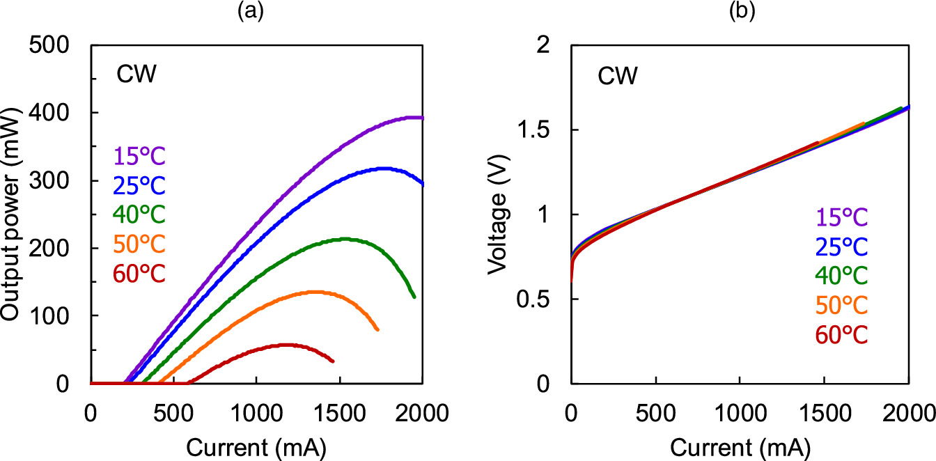
Fig. 2. (a) Light-output-current (L–I) and (b) voltage–current (V–I) characteristics of the fabricated 200-μm-diameter PCSEL under CW conditions from 15 °C to 60 °C.
Download figure:
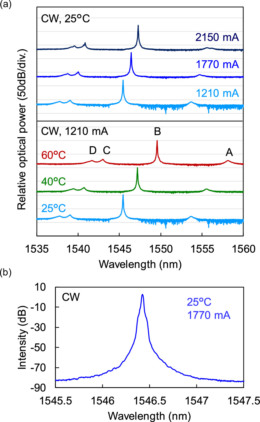
Standard image High-resolution imageIn Fig. 3(a), lasing spectra at various injection currents and temperatures under CW conditions are presented. These spectra were measured using an optical spectrum analyzer. All spectra exhibit single-mode lasing oscillations at around 1550 nm. Four modes labeled A to D in the order of increasing frequency are presented in Fig. 3(a), with mode B identified as the lasing mode; details about the origin of these modes are discussed later. Figure 3(b) shows a magnified spectrum of the peak at 25 °C and an injection current of 1770 mA (corresponding to the conditions of maximum output power). Single-mode oscillation with the peak wavelength of 1546.43 nm, with a full width at half maximum (FWHM) below 0.02 nm (the resolution limit of our analyzer), is clearly observed. The broadening of the spectrum below −20 dB is attributed to the characteristics of the analyzer, and not to the device properties. SMSRs are extracted as a function of injection current and operating temperature, as shown in Fig. 4. Remarkably, high SMSRs exceeding 60 dB are maintained under all examined conditions, even though a slight decrease of the SMSR is observed with increasing current or temperature, which we attribute to the slight increase of the intensity of emission from mode C. Furthermore, these single-mode operations lead to narrow-divergence-angle beams. We have measured the far-field pattern, and the divergence angle is below 1° at an injection current of 800 mA and 25 °C, evaluated by the 1/e2 width.

Fig. 3. (a) Lasing spectra of the fabricated 1550 nm wavelength PCSEL under CW conditions with various injection currents and temperatures, and (b) magnified spectrum around the lasing peak at 25 °C and 1770 mA (corresponding to the conditions of maximum output power).
Download figure:
Standard image High-resolution image
Fig. 4. Side-mode suppression ratio (SMSR) extracted from lasing spectra under CW conditions as a function of (a) operating temperature at an injection current of 1210 mA and (b) injection current at an operating temperature of 25 °C.
Download figure:
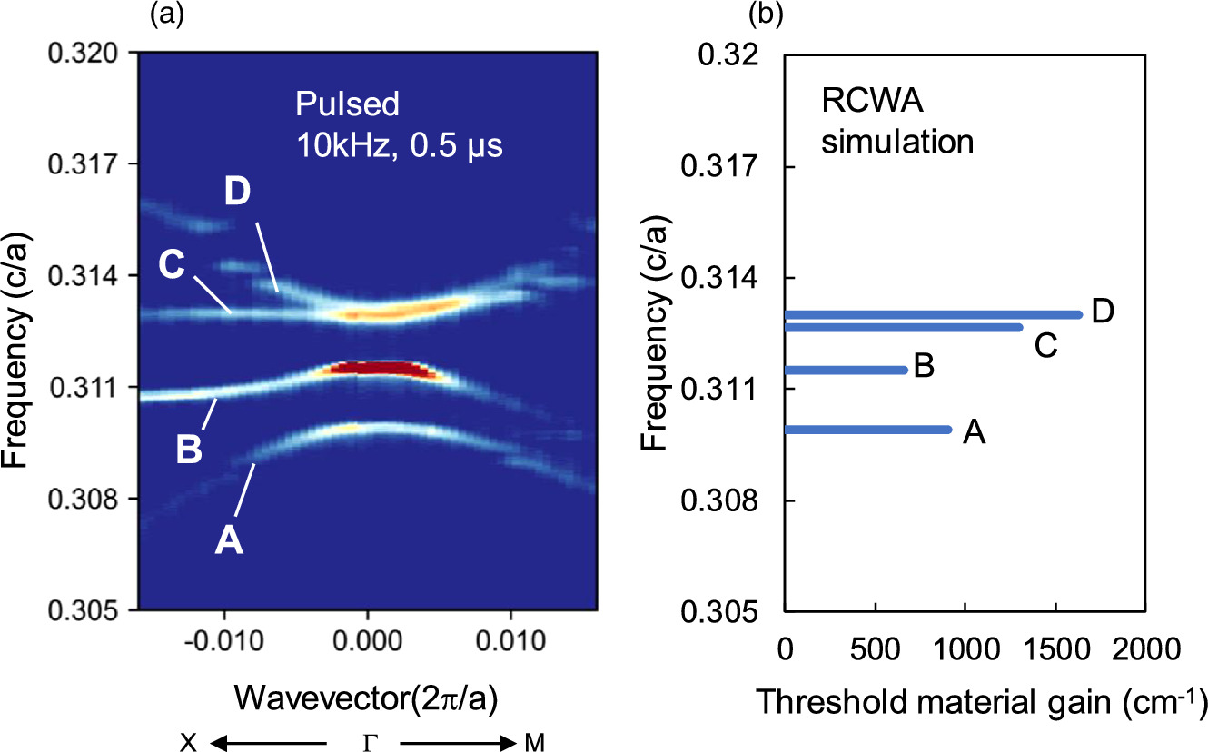
Standard image High-resolution imageNext, we investigate the photonic band structure of the developed PCSEL to gain more insight into its mode stability. Figure 5(a) shows the measured photonic band structure in the vicinity of the Γ point at a sub-threshold injection current under pulsed conditions at room temperature. Four distinct band-edge modes, labeled A–D, are observed,which is consistent with the above-threshold spectra shown in Fig. 3(a). The formation of these four band-edge modes reflects the characteristics of the square-lattice PC structure. 27) To further understand the origin of the stable single-mode operation in mode B, calculations based on rigorous coupled-wave analysis (RCWA) were performed for the PCSEL structure, taking into account the precise shape of the air holes, to reproduce the measured band structure. Subsequently, the threshold material gain (gth) was determined using the following formula:

Here, αv is the vertical radiation constant, α// is the in-plane cavity loss from the periphery of the lasing area, α0 is the intrinsic loss, and Γqw is the optical confinement factor inside the quantum wells.
Fig. 5. (a) Measured photonic band structure of the 1550 nm wavelength PCSEL at a sub-threshold injection current under pulsed conditions with a pulse width of 0.5 μs and a duty cycle of 0.1% at room temperature. (b) Calculated mode frequencies and threshold gains for band-edge modes A–D.
Download figure:
Standard image High-resolution image
Figure 5(b) presents the calculated mode frequencies and threshold material gains for all four band-edge modes. Mode B exhibits the lowest gth among the four modes and thus is the lasing mode. The substantial threshold material gain margin between mode B and the other modes (Δgth) serves as the origin of the stable single-mode operation. Δgth between mode B and mode C, rather than mode A (whose gth is the second lowest), is of particular interest, due to the observed slight decrease of SMSR owing to emission in mode C in Fig. 4. We attribute the onset of emission in mode C to the effect of a temperature distribution that emerges under CW conditions at high injection currents. Specifically, the temperature at the center of the current injection area becomes higher than that at the periphery, resulting in the concomitant emergence of a downward-convex-shaped in-plane band-edge frequency distribution caused by a temperature-borne change of refractive index. 10,28) For mode C, the area surrounding the injection current area acts as a photonic band gap (PBG) that strengthens the in-plane optical confinement. This is in contrast to modes A and B where the current injection area acts as a PBG, resulting in weakened confinement. Nevertheless, our PC in this study provides a sufficiently large Δgth between modes B and C, as shown in Fig. 5(b), which effectively suppresses lasing in mode C. This large Δgth is owed to the substantial difference between the radiation constants of modes B and C, achieved through appropriate adjustment of the air hole sizes, as explained above.
In addition to oscillation on a single band edge, stable oscillation in the single fundamental mode amidst higher-order modes on the same band edge is also crucial. As mentioned above, moderately weakened κ1D L effectively suppresses oscillation in these higher-order modes while maintaining oscillation in the fundamental mode. 25,29) This is because κ1D L is inversely proportional to the amount of light that propagates in-plane to the periphery of a finite-sized device, which determines α//. Since the antinodes of the electric field distributions of the higher-order modes lie closer to this periphery than that of the fundamental mode, the former modes have higher α//. Using 3D coupled-wave theory, 9,30) we calculated the coupling coefficients of our device to be κ1D = 468 cm−1 and κ2D =183 cm−1. The calculated κ1D is comparable to that of our 1300 nm wavelength single-mode PCSELs, whose κ1D is 400–500 cm−1. 20,26) As indicated in the lasing spectra shown in Fig. 3, lasing clearly occurs in the fundamental mode of band-edge B and not in any higher-order modes. This result is attributed to the appropriately designed hole distance d, as well as to the deeply-etched air holes, which increase κ2D to enable robustly 2D oscillation within the cavity.
In summary, we have developed and investigated 1550 nm wavelength InP-based PCSELs with double-lattice PC structures. We have demonstrated highly stable CW single-mode oscillation with a SMSR of over 60 dB at injection currents of up to 2 A and operating temperatures of up to 60 °C, along with a record CW output power exceeding 300 mW and a wall-plug efficiency of 17.3% at 25 °C. Furthermore, the origin of stable single-mode operation has been investigated based on an analysis of photonic band structures. This analysis has indicated that stable oscillation in the fundamental mode of a single band edge is achieved by a large threshold gain margin and moderately weakened in-plane optical coupling of the PC structure. These InP-based PCSELs are promising light sources for applications requiring both high-power and single-mode characteristics, such as optical communications and eye-safe LiDAR.
Acknowledgments
This work was partly carried out under the Programs for Bridging the gap between R&D and the Ideal Society and Generating Economic and Social Value (BRIDGE), Cabinet Office, Japan.